EP1443016A2 - Mikrohergestellte Vorrichtung und Verfahren zu ihrer Herstellung - Google Patents
Mikrohergestellte Vorrichtung und Verfahren zu ihrer Herstellung Download PDFInfo
- Publication number
- EP1443016A2 EP1443016A2 EP03020079A EP03020079A EP1443016A2 EP 1443016 A2 EP1443016 A2 EP 1443016A2 EP 03020079 A EP03020079 A EP 03020079A EP 03020079 A EP03020079 A EP 03020079A EP 1443016 A2 EP1443016 A2 EP 1443016A2
- Authority
- EP
- European Patent Office
- Prior art keywords
- micro
- device substrate
- fabricated
- accordance
- support structure
- Prior art date
- Legal status (The legal status is an assumption and is not a legal conclusion. Google has not performed a legal analysis and makes no representation as to the accuracy of the status listed.)
- Withdrawn
Links
Images


Classifications
-
- G—PHYSICS
- G11—INFORMATION STORAGE
- G11B—INFORMATION STORAGE BASED ON RELATIVE MOVEMENT BETWEEN RECORD CARRIER AND TRANSDUCER
- G11B9/00—Recording or reproducing using a method not covered by one of the main groups G11B3/00 - G11B7/00; Record carriers therefor
- G11B9/10—Recording or reproducing using a method not covered by one of the main groups G11B3/00 - G11B7/00; Record carriers therefor using electron beam; Record carriers therefor
-
- B—PERFORMING OPERATIONS; TRANSPORTING
- B81—MICROSTRUCTURAL TECHNOLOGY
- B81B—MICROSTRUCTURAL DEVICES OR SYSTEMS, e.g. MICROMECHANICAL DEVICES
- B81B7/00—Microstructural systems; Auxiliary parts of microstructural devices or systems
- B81B7/0083—Temperature control
- B81B7/009—Maintaining a constant temperature by heating or cooling
- B81B7/0093—Maintaining a constant temperature by heating or cooling by cooling
Definitions
- MEMS Micro Electro Mechanical Systems
- electromechanical devices such as relays, actuators, sensors, valves, and other transducers.
- electromechanical devices incorporated in a MEMS device can be integrated with integrated circuits providing improved performance over conventional systems.
- Many types of transducers, incorporated into MEMS devices, such as, vacuum sensors, gas flow sensors, infrared detectors, and AC power converters operate, in the detection of, or utilization of, a temperature difference that is isolated from the rest of the integrated circuit (IC). This increased complexity further increases the demands on improving thermal transfer both by maximizing thermal transfer in some cases and minimizing thermal transfer in other cases.
- a vacuum sensor may operate at its maximum efficiency at over a 100° C while associated CMOS circuitry processing the output of the vacuum sensor or controlling some other function may efficiently operate at room temperature or even sub-ambient temperatures such as -25° C.
- CMOS circuitry processing the output of the vacuum sensor or controlling some other function may efficiently operate at room temperature or even sub-ambient temperatures such as -25° C.
- a solution to such a problem results in tradeoffs such as by, increasing the power applied to the vacuum sensor to heat it, while also increasing the cooling power applied to the CMOS circuitry to maintain it at a lower temperature, typically room temperature or below.
- the end result is an electronic device whose performance is compromised
- the inability to control thermal transfer can both, result in a significant increase in power consumption as well as less than optimum performance.
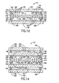
- Fig. 1a is a top view of a micro-fabricated device according to an embodiment of the present invention.
- Fig. 1b is a cross-sectional view of the micro-fabricated device shown in Fig. 1a according to an embodiment of the present invention
- Fig. 1c is a cross-sectional view of the micro-fabricated device shown in Fig. 1a according to an alternate embodiment of the present invention
- Fig. 1d is a cross-sectional view of the micro-fabricated device shown in Fig. 1a according to an alternate embodiment of the present invention
- Fig. 1e is a cross-sectional view of the micro-fabricated device shown in Fig. 1a according to an alternate embodiment of the present invention
- Fig. 2a is a top view of a micro-fabricated device according to an alternate embodiment of the present invention.
- Fig. 2b is a cross-sectional view of the micro-fabricated device shown in Fig. 2a according to an embodiment of the present invention
- Fig. 3a is a top view of a micro-fabricated device according to an alternate embodiment of the present invention.
- Fig. 3b is a cross-sectional view of the micro-fabricated device shown in Fig: 3a according to an embodiment of the present invention
- Fig. 3c is a cross-sectional view of the micro-fabricated device shown in Fig. 3a according to an alternate embodiment of the present invention
- Fig. 4a is a top view of a thermally isolating structure according to an alternate embodiment of the present invention.
- Fig. 4b is a top view of a thermally isolating structure according to an alternate embodiment of the present invention.
- Fig. 4c is a top view of a thermally isolating structure according to an alternate embodiment of the present invention.
- Fig. 5a is a top view of a micro-fabricated device according to an alternate embodiment of the present invention.
- Fig. 5b is a cross-sectional view of the micro-fabricated device shown in Fig. 5a;
- Fig. 6a is a top view of a micro-fabricated device according to an alternate embodiment of the present invention.
- Fig. 6b is a cross-sectional view of the micro-fabricated device shown in Fig. 6a;
- Fig. 7 is a cross-sectional view of a micro-fabricated device having an integrated vacuum device according to an alternate embodiment of the present invention.
- Fig. 8 is a block diagram of an electronic device according to an embodiment of the present invention.
- Fig. 9 is a flow chart of a method of making a micro-fabricated device according to an embodiment of the present invention.
- Fig. 10a-10h are cross-sectional views of various processes used to create embodiments of the present invention.
- thermally isolating structure 120 reduces the thermal conduction between device substrate 130 and support structure 140 while providing mechanical support.
- Device substrate 130 is disposed, within aperture 142 formed in support structure 140, distance G from support structure 140 and thermally isolating structure 120 is thermally coupled to device substrate 130 and support structure 140 at attachment points 121.
- thermally isolating structure 120 has characteristic length or thermal conduction path 118, measured between attachment points 121 that is greater than distance G.
- thermal conduction path 118 is at least twice as long as distance G; however, in alternate embodiments, path 118 may be shorter or longer depending on the particular application in which micro-fabricated device 100 is utilized.
- device substrate 130 may be heated or cooled to a temperature different from the temperature of support structure 140 more efficiently than a straight or shorter conduction path having the same cross-sectional area. Whether device substrate 130 is heated or cooled will depend, for example, on the particular application in which micro-fabricated device 100 will be utilized.
- Device substrate 130, thermally isolating structure 120, and support structure 142 form a substantially planar structure as shown, in a cross-sectional view, in Fig. 1b.
- micro-fabricated device 100 is formed from the same material.
- a silicon wafer may be utilized to form device substrate 130, thermally isolating structure 120, and support structure 140.
- micro-fabricated device 100 may be formed utilizing wafers or substrates made from materials such as glass, ceramic, silicon, gallium arsenide, germanium, indium phosphide, metals, and various polymers to name a few.
- micro-fabricated device 100 will depend on various parameters such as the particular application in which the device will be utilized, both process and operating temperatures, presence or absence of active electronic devices, and the thermal and mechanical properties of the device.
- cross-sectional area 115 of thermally isolating structure 120 may be varied to further tune the thermal conduction of isolating structure 120 by varying the thickness of thermally isolating structure 120.
- micro-fabricated device 100 is formed on a silicon wafer cross-sectional area 115 may have the same thickness as that of device substrate 130 and support structure 140 by utilizing an isotropic etch, as shown in Fig.
- micro-fabricated device 100 of the present invention is shown in a cross-sectional view.
- micro-fabricated device 100 is enclosed in sealed package 110.
- Sealed package 110 is a vacuum package providing additional thermal control, by reducing thermal transfer by convection, between device substrate 130 and the ambient environment.
- sealed package 110 may also be an enclosure providing fluid flow for other applications such as, for example, micro turbines, fuel cells, chemical reactors, and catalytic fuel crackers.
- Device bond structure 180 is formed on support structure 140 over dielectric passivation layer 174 and second dielectric layer 176, which provide electrical isolation.
- Cover or lid bond structures 184 are formed on cover or lid 182
- base or package bottom bond structures 188 are formed on base or package bottom 186.
- device bond structure 180 may utilize a gold-silicon eutectic for bonding the silicon die to a ceramic package or metal can, or it may also utilize a softer lower melting-point solder, these are just a couple of examples of the various materials that may be utilized.
- a frit glass seal may be utilized to attach micro-fabricated device 100 to cover 184 and base 186.
- bond structures 180, 184 and 188 will depend on the particular materials utilized for support structure 140, lid 182, and base 186. Lid 182 and base 186 may utilize various, ceramic, glass, or metal materials or combinations of these materials. The particular material will depend on, for example, the desired pressure to be maintained; the temperature and humidity and other environmental factors to which the micro-fabricated device will be exposed; and the amount of stress that may be imparted to the micro-fabricated device as a result of the packaging process; as well as, the particular sealing technology to be utilized. These same parameters are also considered when determining the material to be utilized as bond structures.
- seal 181 can be made by a variety of techniques such as, for example, thermal compression bonding or brazing, as well as other techniques.
- a low melting-point inorganic oxide such as, for example, lead oxide or boric oxide may also be used for bond structures 180, 184, and 188 to generate seal 181.
- anodic bonding may be utilized to attach micro-fabricated device 100 made out of silicon to a cover and base each either made out of glass or having a glass surface to bond to the silicon.
- the silicon surface of the micro-fabricated device and the glass surface of either the cover or base are placed between two electrodes so that an appropriate polarity voltage is applied across the interface of the two materials. After bonding of the first pair is completed the remaining base or cover is then bonded in the same manner.
- Non-evaporable getter material 190 may also be applied or deposited on various portions of cover 182 and base 186 to provide pumping of residual gases within sealed package 110 during operation of micro-fabricated device 100.
- micro-fabricated device 100 of the present invention is shown in a cross-sectional view.
- micro-fabricated device 100 is enclosed in package 111, that includes reflector layers 193 and 195 that are interposed between device substrate 130 and cover 182 and base 186 respectively.
- package 111 includes a vacuum portion, providing additional thermal control by reducing thermal convection between device substrate 130 and the ambient environment, as well as, a radiation portion, providing further thermal control by reducing thermal losses due to radiation either to or from device substrate 130.
- Device bond structure 180 is formed on support structure 140 over dielectric passivation layer 174 and second dielectric layer 176, which provide electrical isolation.
- Reflector bond structures 196 are formed on first reflector substrate 192 and second reflector substrate 194.
- cover or lid bond structures 184 are formed on cover or lid 182, and base bond structures 188 are formed on base or package bottom 186. Similar materials and processes as described above for the embodiment shown in Fig. 1d may also be utilized, in this embodiment, to form package 111.
- First reflector layer 193 and second reflector layer 195 are deposited on first reflector substrate 192 and second reflector substrate 194 respectively.
- first reflector layer 193 and second reflector layer 195 may be formed from a metal such as gold, aluminum, tungsten, silver, and platinum to name just a few. In alternate embodiments, any material having the appropriate reflectivity in the wavelength region desired may also be utilized. The particular material utilized will depend on various parameters such as temperature of operation, presence or absence of oxygen, or other corrosive material, and the particular application in which micro-fabricated device 100 will be utilized. In this embodiment, first reflector layer 193 and second reflector layer 195 reflect thermal radiation emitted from device substrate 130.
- Reflector substrate interspace region 197 between the cover and top reflector is maintained at a pressure below atmospheric pressure in this embodiment.
- Device interspace region 198 may be maintained at a pressure below atmospheric pressure for those applications utilizing a vacuum such as a vacuum sensor. However, in other embodiments, device interspace region 198 may be maintained at atmospheric or pressures above atmospheric pressures such as for catalytic reactors, or fuel cells. In still other embodiments device interspace region 198 may also be an enclosure providing fluid flow of either a gas or liquid depending on the application such as, for example, micro turbines, fuel cells, heat engines, chemical reactors, and catalytic fuel crackers.
- Non-evaporable getter material 190 may also be applied or deposited on various portions of cover 182 and base 186 to provide pumping of residual gases within reflector substrate interspace region 197 during operation of micro-fabricated device 100.
- Active device 234 includes for example transistors (including thin-film-transistor (TFT) or amorphous silicon transistors), diodes, logic cells, as well as sensors, transducers, electron emitters, bolometers, and superconductoring high Q RF filters to name just a few of the many active devices that may be utilized, either separately or in combination, in the present invention.
- TFT thin-film-transistor
- amorphous silicon transistors active device 234 includes for example transistors (including thin-film-transistor (TFT) or amorphous silicon transistors), diodes, logic cells, as well as sensors, transducers, electron emitters, bolometers, and superconductoring high Q RF filters to name just a few of the many active devices that may be utilized, either separately or in combination, in the present invention.
- active device 234 may also be integrated with various MEMS devices such as microfluidic channels, reactor chambers, micromovers, and actuators to name just a few of the many MEMS devices that may be utilized.
- micro-fabricated device 200 may include a micro mirror disposed on said device substrate 230 including a reflective surface disposed on said mirror.
- a bolometer or other radiation detector having a light absorbing surface disposed on said device substrate 230
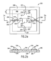
- Device substrate 230 is disposed, within aperture 242 formed in support structure 240, a distance G from support structure 240.
- Thermally isolating structure 220 attaches to device substrate 230 and support structure 240 at attachment points 221 as shown in Fig. 2a.
- thermally isolating structure 220 has characteristic length or thermal conduction path 218 measured between attachment points 221, that is greater than the gap between device substrate 230 and support structure 240 labeled as distance G.
- thermally isolating structure 220 forms an accordion or chevron like structure to reduce the thermal conduction between device substrate 230 and support structure 240, as well as, providing mechanical support for device substrate 230.
- Thermally isolating structure 220 is formed to minimize tension in thermally isolating structure 220 and reduce stress applied to device substrate 230.
- Electrical interconnection trace 224 is formed on thermally isolating structure 220 and electrically couples to substrate electrical trace 235. Whether device substrate 230 is heated or cooled depends, for example, on the particular application in which micro-fabricated device 200 will be utilized.
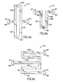
- FIG. 3a an alternate embodiment of micro-fabricated device 300, of the present invention, is shown in a top view.
- device substrate 330 is disposed over support structure 340 forming a vertical structure.
- substrate 330 is separated a distance G from support structure 340.
- thermally isolating structure 320 is attached to substrate attachment surface 332 formed by bottom surface 336 of device substrate 330.
- thermally isolating structure 320 may attach at other points such as for example side surface 337 of device substrate 330.
- thermally isolating structure 320 has characteristic length or thermal conduction path 318, measured between attachment points 321, that is greater than distance G.
- device substrate 330 may be heated or cooled to a temperature different from the temperature of support structure 340 more efficiently than a straight or short conduction path. Whether device substrate 330 is heated or cooled will depend, for example, on the particular application in which micro-fabricated device 300 will be utilized.
- An alternate embodiment, of thermally isolating structure 320 is shown, in a cross-sectional view, in Fig. 3c. In this embodiment, thermally isolating structure 320' includes multiple attachment points 321' on both device substrate 330 and support structure 340. Characteristic length 318' is greater than gap width G.
- thermally isolating structures 420a, 420b, and 420c of the present invention are shown in a top view.
- thermally isolating structures 420a, 420b, 420c include first section 426, second section 427 and folding section 428 forming a folded structure having at least one fold.
- First section 426 and second section 427 are substantially parallel to each other with the three sections 426-428 forming a U shaped structure.
- Thermally isolating structures 420a, 420b, and 420c each include thermal conduction path 418a, 418b, and 418c respectively, that is longer than the straight line distance measured between attachment points 421.
- thermally isolating structures 420a, 420b, and 420c are formed of a single layer having a substantially uniform coefficient of expansion and a substantially uniform composition of matter.
- thermally isolating structures 420a, 420b, and 420c may be formed utilizing two or more layers depending on the particular application in which the micro-fabricated device will be utilized.
- the cross-sectional area of the thermally isolating structures may also be varied; for example, the cross-sectional area at the attachment point 421 at support structure 440 may be thicker than the crass-sectional area at device substrate 430.
- the cross-sectional area may vary at various locations of the thermally isolating structure, such as folding section 428 may be thinner than first or second section 426 or 427.
- thermally isolating structure 520 is formed above or out of this substantially planar structure as shown, in cross-sectional view, in Fig. 5b.
- thermally isolating structure 520 is formed from a different material than device substrate 530 and support structure 540.
- device substrate 530 and support structure 540 may be formed from a silicon wafer and the thermally isolating structures may be formed from a silicon oxide or nitride layer deposited on the silicon wafer.
- thermally isolating structure 520 reduces the thermal conduction between device substrate 530 and support structure 540 while providing mechanical support.
- Device substrate 530 is disposed, within aperture 542 formed in support structure 540, distance G from support structure 540.
- themially isolating structure 520 includes thermal conduction path 518, measured between attachment points 521 that is greater than distance G.
- Cross-sectional area 515 of thermally isolating structure 520 in this embodiment, is uniform providing a uniform coefficient of expansion, as well as, uniform composition of matter.
- cross-sectional area 515 of thermally isolating structure 520 may be varied to further tune the thermal conduction of isolating structure 520 by varying the thickness of thermally isolating structure 520.
- the cross-sectional composition may also be varied, such as, by varying the stoichiometry of, for example, a silicon dioxide or silicon nitride layer varying from oxygen or nitrogen deficient to oxygen or nitrogen rich either along the thermal conduction path 518 or across or through cross-sectional area 515 or some combination thereof.
- a thermally isolating structure formed from such a layer or layers would have both a non-uniform thermal coefficient of expansion, as well as, a non-uniform composition of matter.
- thermally isolating structure 520 may be formed of any suitable material such as a metal, a semiconductor, an inorganic, or a polymeric material or combinations of these materials.
- an electroplated or sputter deposited metal film, or a spin coated or screen-printed polyimide benzocylcobutene layer are just a couple of materials that may be utilized. The particular material used will depend on the particular application in which micro-fabricated device 500 will be utilized.
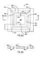
- thermally isolating structure 620 forms an annular structure around device substrate 630.
- Thermally isolating structure 620 reduces the thermal conduction between device substrate 630 and support structure 640 while providing mechanical support.
- Device substrate 630 is disposed, within aperture 642 formed in support structure 640, distance G from support structure 640.
- thermally isolating structure 620 includes thermal conduction path 618measured between corner attachment point 621 and attachment points 621' on device substrate 630, where thermal conduction path length 618 is greater than distance G.
- Cross-sectional view 6b illustrates the substantially planar structure of this embodiment.
- thermally isolating structure 620 may also be formed out of the substantially planer structure formed by the device substrate and support structure as illustrated in the embodiment shown in Figs. 5a and 5b.
- Fig. 7 is an exemplary embodiment of a micro-fabricated device having integrated vacuum device 702 that includes anode surface 750 such as a display screen or a mass storage device that is affected by electrons 762 when they are formed into a focused beam 764.
- Thermally insulating structure 720 reduces the thermal conduction between device substrate 730 and support structure 740 while providing mechanical support.
- Device substrate 730 is disposed, within aperture 742 formed in support structure 740.
- Anode surface 750 is held at a predetermined distance from second electron lens element 752.
- Micro-fabricated device 700 is enclosed in a vacuum package (not shown).
- integrated vacuum device 702 is shown in a simplified block form and may be any of the electron emitter structures well known in the art such as a Spindt tip or flat emitter structure.
- Second lens element 752 acts as a ground shield.
- Vacuum device 702 is disposed over at least a portion of device substrate 730.
- First insulating or dielectric layer 754 electrically isolates second lens element 752 from first lens element 756.
- Second insulating layer 758 electrically isolates first lens element 756 from vacuum device 702.
- more than two lens elements may be utilized to provide, for example, an increased intensity of electron emission or increased focusing ability for electron beam 764. Both the lens elements and dielectrics are fabricated utilizing conventional semiconductor processing equipment.
- an array of pixels are formed on anode surface 750, which further are typically arranged in a red, blue, green order, however, the array of pixels may also be a monochromatic color.
- An array of emitters are formed on device substrate 630 where each element of the emitter array has one or more integrated vacuum devices acting as an electron emitter.
- Application of the appropriate signals to an electron lens structure including first and second electron lens 752 and 756 generates the necessary field gradient to focus electrons 762 emitted from vacuum device 702 and generate focused beam 764 on anode surface 750.
- anode surface 750 typically includes a phase-change material or storage medium that is affected by the energy of focused beam 764.
- the phase-change material generally is able to change from a crystalline to an amorphous state (not shown) by using a high power level of focused beam 764 and rapidly decreasing the power level of focused beam 764.
- the phase-change material is able to change from an amorphous state to a crystalline state (not shown) by using a high power level of focused beam 764 and slowly decreasing the power level so that the media surface has time to anneal to the crystalline state.
- This change in phase is utilized to form a storage area on anode surface 750 that may be in one of a plurality of states depending on the power level of focused beam 764 used. These different states represent information stored in that storage area.
- phase change media is germanium telluride (GeTe) and ternary alloys based on GeTe.
- the mass storage device also contains electronic circuitry (not shown) to move anode surface 750 in a first and preferably second direction relative to focused beam 764, to allow a single integrated vacuum device 702, to read and write multiple locations on anode surface 750.
- electronic circuitry to move anode surface 750 in a first and preferably second direction relative to focused beam 764, to allow a single integrated vacuum device 702, to read and write multiple locations on anode surface 750.
- a lower-energy focused beam 764 strikes media surface 750 that causes electrons to flow through the media substrate 760, and a reader circuit (not shown) detects them. The amount of current detected is dependent on the state, amorphous or crystalline, of the media surface struck by focused beam 764.
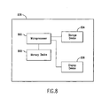
- Electronic device 808 such as a computer system, video game, Internet appliance terminal, MP3 player, cellular phone, or personal digital assistant to name just a few is shown.
- Electronic device 808 includes microprocessor 866, such as an Intel processor sold under the name "Pentium Processor,” or compatible processor. Many other processors exist and may also be utilized.
- Microprocessor 866 is electrically coupled to memory device 868 that includes processor readable memory that is capable of holding computer executable commands or instructions used by the microprocessor 866 to control data, input/output functions, or both.
- Memory device 868 may also store data that is manipulated by microprocessor 866.
- Microprocessor 866 is also electrically coupled either to storage device 804, or display device 806 or both.
- Microprocessor 866, memory device 868, storage device 804, and display device 806 each may contain an embodiment of the present invention as exemplified in earlier described figures and text showing device substrates having thermally isolating structures.
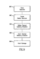
- FIG. 9 a flow diagram of a method of manufacturing a micro-fabricated device, according to an embodiment of the present invention, is shown.
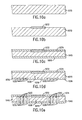
- Figs. 10a-10h are illustrations of the processes utilized to create a micro-fabricated device, and are shown only to better clarify and understand the invention. Actual dimensions are not to scale and some features are exaggerated to more clearly point out the process.
- Substrate forming process 990 is utilized to form the substrate on which the device substrate and the support structure will be created.
- wafer 1070 is a single crystal silicon substrate having a thickness of about 200-800 microns as shown in a cross-sectional view in Fig. 10a.
- both other materials and thicknesses may be utilized.
- gallium arsenide, glass, and polymer substrates are just a few of the alternate materials that may be used in the present invention.
- wafer 1070 is not restricted to typical wafer sizes, and may be a polymer sheet or film, or glass sheet, or even a single crystal sheet or substrate handled in a different form and size than that of conventional silicon wafers.
- Device structure creation process 992 is utilized to create MEMS structures or active devices or both 1072 on the micro-fabricated device as shown in a cross-sectional view in Fig. 10b.
- MEMS structures may include transducers, actuators, sensors, and valves to name a few.
- device structure creation process 992 also includes creating various electronic circuits such as for example, transistors, logic circuits, memory cells as well as passive devices such as capacitors, resistors, and inductors. For clarity these devices are represented as a single layer 1072 in Fig. 10b. The particular devices and circuits created will depend on the particular application in which the micro-fabricated device will be utilized.
- the electronic circuits are fabricated utilizing conventional IC processing equipment and processes. Bulk or surface micromachining or combinations of both are utilized to form the MEMS structures.
- an integrated pressure sensor is typically fabricated using IC processing to create the driving and analysis circuits followed by micromachining from the back side of the wafer to create a micromachined diaphragm.
- Other examples include infrared sensing arrays formed utilizing IC processing to form thermopiles and other circuitry followed by micromachining to create the sensing array, or fabricating an amplifier operating in the radio frequency range utilizing CMOS technology to fabricate the IC amplifier and micromachining to produce an inductor with the proper resonance frequency.
- Device structure creation process 992 also includes deposition and pattern generation for electrical traces and interconnect pads providing for the routing of signals and power to various portions of the micro-fabricated device.
- Thermally isolating structure definition process 994 is utilized to define the shape or structure of the thermally isolating structures such as the desired thermal conduction path and attachment points.
- thermally isolating structure definition process 994 may also be utilized to define the device substrate, and the support structure.
- Dielectric passivation layer 1074 and etch defining layer 1076 are deposited over silicon substrate 1070 and MEMS or electronic devices or both 1072 as shown, in a cross-seetional view, in Fig 10c. In alternate embodiments dielectric passivation layer 1074 and etch defining layer 1076 may be deposited during device structure creation process depending on the particular devices fabricated as well as the particular application in which the micro-fabricated device will be utilized.
- Deposition techniques such as plasma enhanced chemical vapor deposition (PECVD), sputter deposition, chemical vapor deposition may be utilized to deposit refractory dielectrics such as silicon oxide, silicon nitride, or silicon carbide to name just a few examples.
- PECVD plasma enhanced chemical vapor deposition
- chemical vapor deposition may be utilized to deposit refractory dielectrics such as silicon oxide, silicon nitride, or silicon carbide to name just a few examples.
- spin coating, curtain coating, or screen printing may also be utilized to form a polymer dielectric passivation layer such as polyimides, or benzocyclobutene are just a couple of examples.
- planarizing processes such as chemical mechanical processing (CMP) may be utilized for those applications desiring a planarized dielectric layer.
- Etch defining layer 1076 is deposited on the back or opposite side of silicon substrate 1070 as shown in a cross-sectional view in Fig. 10c.
- etch defining layer 1076 is a silicon nitride layer, however, in alternate embodiments, other refractory materials such a silicon oxide or silicon carbide or polymeric materials such as a photo resist or polyimide may also be utilized depending on various parameters such as the particular substrate material utilized as well as the particular etchant utilized to form the thermally isolating structure.
- Etch defining layer 1076 is then patterned utilizing conventional photolithographic technologies and processes to form openings 1078 as shown, in a cross-sectional view, in Fig. 10d.
- the size and shape of opening 1078 also depends on various parameters such as particular etchant utilized to etch wafer 1070 as well as the wafer or substrate material.
- opening 1078 may be formed in dielectric passivation layer 1074 or both.
- Thermally isolating structure formation process 996 is utilized to form, or generally etch, wafer 1070 and generate thermally isolating structure 1020, device substrate 1030, and support structure 1040.
- a dry etch may be used when vertical or orthogonal sidewalls are desired.
- an anistropic wet etch such as potassium hyrdoxide (KOH) may be used to etch a (110) oriented silicon wafer to also produce vertical sidewalls.
- KOH potassium hyrdoxide
- an anisotropic wet etch such as KOH or tetra methyl ammonium hydroxide (TMAH)
- TMAH tetra methyl ammonium hydroxide
- combinations of wet and dry etch may also be utilized when moce complex structures are desired.
- other processes such as laser ablation, reactive ion etching, ion milling including focused ion beam patterning may also be utilized to form thermally isolating structure 1020, device substrate 1030, and support structure 1040 as shown in Fig. 10e.
- dielectric passivation layer 1074 and etch defining layer 1076 may be removed as shown in Fig. 10f.
- dielectric passivation layer 1074 and etch defining layer 1076 remain on support structure 1040 to illustrate additional packaging steps, however, in alternate embodiments these layers may be completely removed or left in selective areas, depending on various parameters such as the desired thermal and electrical isolation properties on various portions of the micro-fabricated device.
- Package forming process 998 is utilized to create an optional vacuum package that reduces heating or cooling by convection, depending on the particular application in which the micro-fabricated device will be utilized.
- device bond structure 1080 is formed on support structure 1040 over dielectric passivation layer 1074 and etch defining layer 1076.
- Dielectric passivation layer 1074 and etch defining layer 1076 provide electrical isolation, as well as, reducing the thermal conduction, between the package and support structure 1040.
- Device bond structure 1080 may be a gold-silicon etutectic for bonding a silicon die to a ceramic package or metal can, or it may be a softer lower melting point solder, to name just a couple of examples of the various materials that may be utilized.
- Cover or lid bond structure 1084 is formed on cover or lid 1082, and base or package bottom bond structure 1088 is formed on base or package bottom 1086.
- the material utilized for device bond structure 1080, cover bond structure 1084 and base bond structure 1088 depends on the particular materials utilized for wafer 1070, cover 1082, and base 1086.
- Cover 1082 and base 1086 may utilize various, ceramic, glass, or metal materials.
- the particular material will depend, for example, on the desired pressure to be maintained, on the temperature and humidity and other environmental factors to which the micro-fabricated device will be exposed, and on the amount of stress that may be imparted to the micro-fabricated device as a result of the packaging process; as well as; the particular sealing technology to be utilized. These same parameters are also considered when determining the material to be utilized as bond structures.
- Seal 1081 can be made by a variety of techniques including thermal compression, brazing, anodic bonding, as well as other techniques.
Applications Claiming Priority (2)
| Application Number | Priority Date | Filing Date | Title |
|---|---|---|---|
| US353332 | 2003-01-29 | ||
| US10/353,332 US20040147056A1 (en) | 2003-01-29 | 2003-01-29 | Micro-fabricated device and method of making |
Publications (2)
| Publication Number | Publication Date |
|---|---|
| EP1443016A2 true EP1443016A2 (de) | 2004-08-04 |
| EP1443016A3 EP1443016A3 (de) | 2006-04-19 |
Family
ID=32655523
Family Applications (1)
| Application Number | Title | Priority Date | Filing Date |
|---|---|---|---|
| EP03020079A Withdrawn EP1443016A3 (de) | 2003-01-29 | 2003-09-04 | Mikrohergestellte Vorrichtung und Verfahren zu ihrer Herstellung |
Country Status (4)
| Country | Link |
|---|---|
| US (1) | US20040147056A1 (de) |
| EP (1) | EP1443016A3 (de) |
| JP (1) | JP2004235638A (de) |
| TW (1) | TWI295275B (de) |
Cited By (5)
| Publication number | Priority date | Publication date | Assignee | Title |
|---|---|---|---|---|
| WO2006067784A1 (en) * | 2004-12-23 | 2006-06-29 | Rafael Armament Development Authority Ltd. | Chip packaging |
| US7490947B2 (en) | 2005-12-16 | 2009-02-17 | Fraunhofer-Gesellschaft Zur Foerderung Der Angewandten Forschung E.V. | Microoptic reflecting component |
| DE102006059091B4 (de) * | 2005-12-16 | 2011-03-31 | Fraunhofer-Gesellschaft zur Förderung der angewandten Forschung e.V. | Mikrooptisches reflektierendes Bauelement und dessen Verwendung |
| US8455287B2 (en) | 2005-05-27 | 2013-06-04 | Semiconductor Energy Laboratory Co., Ltd. | Method for manufacturing semiconductor device including microstructure |
| EP2331454A4 (de) * | 2008-05-13 | 2014-11-26 | Integrated Sensing Systems Inc | Verfahren zur herstellung von mikrofluidhalbleiterbauelementen und dadurch hergestellte bauelemente |
Families Citing this family (98)
| Publication number | Priority date | Publication date | Assignee | Title |
|---|---|---|---|---|
| US6674562B1 (en) | 1994-05-05 | 2004-01-06 | Iridigm Display Corporation | Interferometric modulation of radiation |
| US8014059B2 (en) | 1994-05-05 | 2011-09-06 | Qualcomm Mems Technologies, Inc. | System and method for charge control in a MEMS device |
| US7532377B2 (en) * | 1998-04-08 | 2009-05-12 | Idc, Llc | Movable micro-electromechanical device |
| WO1999052006A2 (en) | 1998-04-08 | 1999-10-14 | Etalon, Inc. | Interferometric modulation of radiation |
| US8928967B2 (en) | 1998-04-08 | 2015-01-06 | Qualcomm Mems Technologies, Inc. | Method and device for modulating light |
| WO2003007049A1 (en) | 1999-10-05 | 2003-01-23 | Iridigm Display Corporation | Photonic mems and structures |
| US6534850B2 (en) * | 2001-04-16 | 2003-03-18 | Hewlett-Packard Company | Electronic device sealed under vacuum containing a getter and method of operation |
| US7781850B2 (en) | 2002-09-20 | 2010-08-24 | Qualcomm Mems Technologies, Inc. | Controlling electromechanical behavior of structures within a microelectromechanical systems device |
| TW570896B (en) | 2003-05-26 | 2004-01-11 | Prime View Int Co Ltd | A method for fabricating an interference display cell |
| US20050130319A1 (en) * | 2003-12-15 | 2005-06-16 | Xerox Corporation | Molecular binding event detection using separation channels |
| US7706050B2 (en) | 2004-03-05 | 2010-04-27 | Qualcomm Mems Technologies, Inc. | Integrated modulator illumination |
| US7164520B2 (en) | 2004-05-12 | 2007-01-16 | Idc, Llc | Packaging for an interferometric modulator |
| US20060009038A1 (en) * | 2004-07-12 | 2006-01-12 | International Business Machines Corporation | Processing for overcoming extreme topography |
| US7889163B2 (en) | 2004-08-27 | 2011-02-15 | Qualcomm Mems Technologies, Inc. | Drive method for MEMS devices |
| US7289259B2 (en) | 2004-09-27 | 2007-10-30 | Idc, Llc | Conductive bus structure for interferometric modulator array |
| US7653371B2 (en) | 2004-09-27 | 2010-01-26 | Qualcomm Mems Technologies, Inc. | Selectable capacitance circuit |
| US20060076634A1 (en) | 2004-09-27 | 2006-04-13 | Lauren Palmateer | Method and system for packaging MEMS devices with incorporated getter |
| US7920135B2 (en) | 2004-09-27 | 2011-04-05 | Qualcomm Mems Technologies, Inc. | Method and system for driving a bi-stable display |
| US7813026B2 (en) | 2004-09-27 | 2010-10-12 | Qualcomm Mems Technologies, Inc. | System and method of reducing color shift in a display |
| US7843410B2 (en) | 2004-09-27 | 2010-11-30 | Qualcomm Mems Technologies, Inc. | Method and device for electrically programmable display |
| US7675669B2 (en) | 2004-09-27 | 2010-03-09 | Qualcomm Mems Technologies, Inc. | Method and system for driving interferometric modulators |
| US7701631B2 (en) | 2004-09-27 | 2010-04-20 | Qualcomm Mems Technologies, Inc. | Device having patterned spacers for backplates and method of making the same |
| US7668415B2 (en) | 2004-09-27 | 2010-02-23 | Qualcomm Mems Technologies, Inc. | Method and device for providing electronic circuitry on a backplate |
| US7724993B2 (en) | 2004-09-27 | 2010-05-25 | Qualcomm Mems Technologies, Inc. | MEMS switches with deforming membranes |
| US8124434B2 (en) | 2004-09-27 | 2012-02-28 | Qualcomm Mems Technologies, Inc. | Method and system for packaging a display |
| US7355780B2 (en) | 2004-09-27 | 2008-04-08 | Idc, Llc | System and method of illuminating interferometric modulators using backlighting |
| US7424198B2 (en) | 2004-09-27 | 2008-09-09 | Idc, Llc | Method and device for packaging a substrate |
| US7420725B2 (en) | 2004-09-27 | 2008-09-02 | Idc, Llc | Device having a conductive light absorbing mask and method for fabricating same |
| US7936497B2 (en) | 2004-09-27 | 2011-05-03 | Qualcomm Mems Technologies, Inc. | MEMS device having deformable membrane characterized by mechanical persistence |
| US7679627B2 (en) | 2004-09-27 | 2010-03-16 | Qualcomm Mems Technologies, Inc. | Controller and driver features for bi-stable display |
| US8878825B2 (en) | 2004-09-27 | 2014-11-04 | Qualcomm Mems Technologies, Inc. | System and method for providing a variable refresh rate of an interferometric modulator display |
| US8008736B2 (en) | 2004-09-27 | 2011-08-30 | Qualcomm Mems Technologies, Inc. | Analog interferometric modulator device |
| US7372613B2 (en) | 2004-09-27 | 2008-05-13 | Idc, Llc | Method and device for multistate interferometric light modulation |
| US7944599B2 (en) | 2004-09-27 | 2011-05-17 | Qualcomm Mems Technologies, Inc. | Electromechanical device with optical function separated from mechanical and electrical function |
| US7532195B2 (en) | 2004-09-27 | 2009-05-12 | Idc, Llc | Method and system for reducing power consumption in a display |
| US7710629B2 (en) | 2004-09-27 | 2010-05-04 | Qualcomm Mems Technologies, Inc. | System and method for display device with reinforcing substance |
| US8310441B2 (en) | 2004-09-27 | 2012-11-13 | Qualcomm Mems Technologies, Inc. | Method and system for writing data to MEMS display elements |
| US7692839B2 (en) | 2004-09-27 | 2010-04-06 | Qualcomm Mems Technologies, Inc. | System and method of providing MEMS device with anti-stiction coating |
| US7916103B2 (en) | 2004-09-27 | 2011-03-29 | Qualcomm Mems Technologies, Inc. | System and method for display device with end-of-life phenomena |
| US7583429B2 (en) | 2004-09-27 | 2009-09-01 | Idc, Llc | Ornamental display device |
| US7893919B2 (en) | 2004-09-27 | 2011-02-22 | Qualcomm Mems Technologies, Inc. | Display region architectures |
| US7719500B2 (en) | 2004-09-27 | 2010-05-18 | Qualcomm Mems Technologies, Inc. | Reflective display pixels arranged in non-rectangular arrays |
| US7136213B2 (en) | 2004-09-27 | 2006-11-14 | Idc, Llc | Interferometric modulators having charge persistence |
| US7684104B2 (en) | 2004-09-27 | 2010-03-23 | Idc, Llc | MEMS using filler material and method |
| US7808703B2 (en) | 2004-09-27 | 2010-10-05 | Qualcomm Mems Technologies, Inc. | System and method for implementation of interferometric modulator displays |
| US7045885B1 (en) * | 2004-12-09 | 2006-05-16 | Hewlett-Packard Development Company, L.P. | Placement of absorbing material in a semiconductor device |
| US7528061B2 (en) * | 2004-12-10 | 2009-05-05 | L-3 Communications Corporation | Systems and methods for solder bonding |
| FR2879819B1 (fr) * | 2004-12-21 | 2007-02-23 | Ulis Soc Par Actions Simplifie | Composant de detection de rayonnements electromagnetiques notamment infrarouges |
| US7920136B2 (en) | 2005-05-05 | 2011-04-05 | Qualcomm Mems Technologies, Inc. | System and method of driving a MEMS display device |
| US7948457B2 (en) | 2005-05-05 | 2011-05-24 | Qualcomm Mems Technologies, Inc. | Systems and methods of actuating MEMS display elements |
| KR20080027236A (ko) | 2005-05-05 | 2008-03-26 | 콸콤 인코포레이티드 | 다이나믹 드라이버 ic 및 디스플레이 패널 구성 |
| JP2007152554A (ja) * | 2005-05-27 | 2007-06-21 | Semiconductor Energy Lab Co Ltd | 半導体装置 |
| US8217473B2 (en) * | 2005-07-29 | 2012-07-10 | Hewlett-Packard Development Company, L.P. | Micro electro-mechanical system packaging and interconnect |
| US8391630B2 (en) | 2005-12-22 | 2013-03-05 | Qualcomm Mems Technologies, Inc. | System and method for power reduction when decompressing video streams for interferometric modulator displays |
| US7795061B2 (en) | 2005-12-29 | 2010-09-14 | Qualcomm Mems Technologies, Inc. | Method of creating MEMS device cavities by a non-etching process |
| US7916980B2 (en) | 2006-01-13 | 2011-03-29 | Qualcomm Mems Technologies, Inc. | Interconnect structure for MEMS device |
| US8194056B2 (en) | 2006-02-09 | 2012-06-05 | Qualcomm Mems Technologies Inc. | Method and system for writing data to MEMS display elements |
| US7903047B2 (en) | 2006-04-17 | 2011-03-08 | Qualcomm Mems Technologies, Inc. | Mode indicator for interferometric modulator displays |
| US7711239B2 (en) | 2006-04-19 | 2010-05-04 | Qualcomm Mems Technologies, Inc. | Microelectromechanical device and method utilizing nanoparticles |
| US8049713B2 (en) | 2006-04-24 | 2011-11-01 | Qualcomm Mems Technologies, Inc. | Power consumption optimized display update |
| JP4720599B2 (ja) * | 2006-04-24 | 2011-07-13 | パナソニック電工株式会社 | 赤外線センサ |
| US7649671B2 (en) | 2006-06-01 | 2010-01-19 | Qualcomm Mems Technologies, Inc. | Analog interferometric modulator device with electrostatic actuation and release |
| US7702192B2 (en) | 2006-06-21 | 2010-04-20 | Qualcomm Mems Technologies, Inc. | Systems and methods for driving MEMS display |
| US7835061B2 (en) | 2006-06-28 | 2010-11-16 | Qualcomm Mems Technologies, Inc. | Support structures for free-standing electromechanical devices |
| US7777715B2 (en) | 2006-06-29 | 2010-08-17 | Qualcomm Mems Technologies, Inc. | Passive circuits for de-multiplexing display inputs |
| US7527998B2 (en) | 2006-06-30 | 2009-05-05 | Qualcomm Mems Technologies, Inc. | Method of manufacturing MEMS devices providing air gap control |
| US8614110B1 (en) * | 2006-07-25 | 2013-12-24 | The United States Of America As Represented By The Secretary Of The Navy | Method for fabricating a dual-crystalline silicon suspension system using pre-fabricated cavities |
| US7767483B1 (en) * | 2006-07-25 | 2010-08-03 | The United States Of America As Represented By The Secretary Of The Navy | Dual-suspension system for MEMS-based devices and method for fabricating same |
| US7763546B2 (en) | 2006-08-02 | 2010-07-27 | Qualcomm Mems Technologies, Inc. | Methods for reducing surface charges during the manufacture of microelectromechanical systems devices |
| JP5114898B2 (ja) * | 2006-09-07 | 2013-01-09 | 日産自動車株式会社 | パッケージ型電子部品及びパッケージ型電子部品の製造方法 |
| JP2008132583A (ja) | 2006-10-24 | 2008-06-12 | Seiko Epson Corp | Memsデバイス |
| US20080128901A1 (en) * | 2006-11-30 | 2008-06-05 | Peter Zurcher | Micro-electro-mechanical systems device and integrated circuit device integrated in a three-dimensional semiconductor structure |
| US7719752B2 (en) | 2007-05-11 | 2010-05-18 | Qualcomm Mems Technologies, Inc. | MEMS structures, methods of fabricating MEMS components on separate substrates and assembly of same |
| JP5374077B2 (ja) * | 2008-06-16 | 2013-12-25 | ローム株式会社 | Memsセンサ |
| JP2010098518A (ja) * | 2008-10-16 | 2010-04-30 | Rohm Co Ltd | Memsセンサの製造方法およびmemsセンサ |
| US8257119B2 (en) * | 2008-12-19 | 2012-09-04 | Honeywell International | Systems and methods for affixing a silicon device to a support structure |
| US8736590B2 (en) | 2009-03-27 | 2014-05-27 | Qualcomm Mems Technologies, Inc. | Low voltage driver scheme for interferometric modulators |
| EP2435355B1 (de) * | 2009-05-29 | 2018-10-24 | DigitalOptics Corporation MEMS | Mechanische isolierung für elektrische mems-kontakte |
| US8471206B1 (en) * | 2009-07-14 | 2013-06-25 | Flir Systems, Inc. | Infrared detector vacuum test systems and methods |
| US20110042137A1 (en) * | 2009-08-18 | 2011-02-24 | Honeywell International Inc. | Suspended lead frame electronic package |
| CN102834761A (zh) | 2010-04-09 | 2012-12-19 | 高通Mems科技公司 | 机电装置的机械层及其形成方法 |
| EP2455332B1 (de) * | 2010-11-19 | 2014-02-12 | Imec | Verfahren zur Herstellung einer temporären Kappe auf einem MEMS-Bauteil |
| US8963159B2 (en) | 2011-04-04 | 2015-02-24 | Qualcomm Mems Technologies, Inc. | Pixel via and methods of forming the same |
| US9134527B2 (en) | 2011-04-04 | 2015-09-15 | Qualcomm Mems Technologies, Inc. | Pixel via and methods of forming the same |
| CN103121658B (zh) * | 2011-11-21 | 2015-10-28 | 水木智芯科技(北京)有限公司 | 电容式三轴微陀螺仪的硅外延制造方法 |
| DE102012005546A1 (de) | 2012-03-21 | 2013-09-26 | Fraunhofer-Gesellschaft zur Förderung der angewandten Forschung e.V. | Mikrospiegelanordnung und Verfahren zur Herstellung einer Mikrospiegelanordnung |
| US20130264755A1 (en) * | 2012-04-05 | 2013-10-10 | Honeywell International Inc. | Methods and systems for limiting sensor motion |
| CN105103292A (zh) * | 2012-10-01 | 2015-11-25 | 贾斯汀·佩恩 | 单片集成光电元件的方法 |
| DE102013214746A1 (de) * | 2013-07-29 | 2014-08-07 | Carl Zeiss Smt Gmbh | Optisches System sowie Verfahren zum Herstellen derselben |
| JP2014041164A (ja) * | 2013-12-05 | 2014-03-06 | New Cosmos Electric Corp | ガス検知素子 |
| US9851256B2 (en) | 2014-06-26 | 2017-12-26 | MP High Tech Solutions Pty Ltd | Apparatus and method for electromagnetic radiation sensing |
| US9810581B1 (en) | 2014-07-28 | 2017-11-07 | MP High Tech Solutions Pty Ltd | Micromechanical device for electromagnetic radiation sensing |
| KR101540070B1 (ko) | 2014-10-27 | 2015-07-29 | 삼성전자주식회사 | 패키지 기판 및 반도체 패키지의 제조방법 |
| US9868628B2 (en) | 2016-03-10 | 2018-01-16 | Taiwan Semiconductor Manufacturing Company, Ltd. | Method and structure for CMOS-MEMS thin film encapsulation |
| US10273141B2 (en) * | 2016-04-26 | 2019-04-30 | Taiwan Semiconductor Manufacturing Co., Ltd. | Rough layer for better anti-stiction deposition |
| US10112826B2 (en) * | 2016-11-29 | 2018-10-30 | Taiwan Semiconductor Manufacturing Co., Ltd. | Method for forming micro-electro-mechanical system (MEMS) device structure |
| US10175113B2 (en) * | 2017-04-12 | 2019-01-08 | Raytheon Company | Thermal protection mechanisms for uncooled microbolometers |
| CN109560054A (zh) * | 2018-12-17 | 2019-04-02 | 厦门大学 | 一种应用于芯片散热的金属微通道热沉结构及其制造方法 |
Citations (10)
| Publication number | Priority date | Publication date | Assignee | Title |
|---|---|---|---|---|
| US5307311A (en) * | 1990-11-02 | 1994-04-26 | Sliwa Jr John W | Microvibratory memory device |
| US5451371A (en) * | 1994-06-09 | 1995-09-19 | Ford Motor Company | High-sensitivity, silicon-based, microcalorimetric gas sensor |
| US5536988A (en) * | 1993-06-01 | 1996-07-16 | Cornell Research Foundation, Inc. | Compound stage MEM actuator suspended for multidimensional motion |
| US5583373A (en) * | 1994-03-07 | 1996-12-10 | National Semiconductor Corporation | Apparatus for achieving mechanical and thermal isolation of portions of integrated monolithic circuits |
| US5648618A (en) * | 1993-10-18 | 1997-07-15 | Armand P. Neukermans | Micromachined hinge having an integral torsion sensor |
| US6300632B1 (en) * | 1999-10-14 | 2001-10-09 | The Regents Of The University Of Michigan | Uncooled infrared focal plane imager and microelectromechanical infrared detector for use therein |
| US6359276B1 (en) * | 1998-10-21 | 2002-03-19 | Xiang Zheng Tu | Microbolom infrared sensors |
| US20020122373A1 (en) * | 2001-03-02 | 2002-09-05 | Marshall Daniel R. | Ultra-high density storage device with resonant scanning micromover |
| US20020173032A1 (en) * | 2001-02-16 | 2002-11-21 | Quanbo Zou | Miniaturized thermal cycler |
| US20020193036A1 (en) * | 2001-06-14 | 2002-12-19 | Benning Paul J. | Focusing lens for electron emitter |
Family Cites Families (11)
| Publication number | Priority date | Publication date | Assignee | Title |
|---|---|---|---|---|
| US626512A (en) * | 1899-06-06 | Half to george j | ||
| US4257061A (en) * | 1977-10-17 | 1981-03-17 | John Fluke Mfg. Co., Inc. | Thermally isolated monolithic semiconductor die |
| JPH09506712A (ja) * | 1993-12-13 | 1997-06-30 | ハネウエル・インコーポレーテッド | 赤外線デバイス用集積シリコン真空マイクロパッケージ |
| US5426303A (en) * | 1994-04-29 | 1995-06-20 | Texas Instruments Incorporated | Thermal isolation structure for hybrid thermal detectors |
| US5600175A (en) * | 1994-07-27 | 1997-02-04 | Texas Instruments Incorporated | Apparatus and method for flat circuit assembly |
| US6091050A (en) * | 1997-11-17 | 2000-07-18 | Roxburgh Limited | Thermal microplatform |
| EP1203208A1 (de) * | 1999-07-30 | 2002-05-08 | Xactix, Inc. | Wärmeisolierung mit vertikaler struktur |
| US6569754B2 (en) * | 2000-08-24 | 2003-05-27 | The Regents Of The University Of Michigan | Method for making a module including a microplatform |
| US6701038B2 (en) * | 2001-03-05 | 2004-03-02 | The Microoptical Corporation | Micro-electromechanical optical switch assembly for optical data networks |
| WO2002079853A1 (en) * | 2001-03-16 | 2002-10-10 | Corning Intellisense Corporation | Electrostatically actuated micro-electro-mechanical devices and method of manufacture |
| US6722197B2 (en) * | 2001-06-19 | 2004-04-20 | Honeywell International Inc. | Coupled micromachined structure |
-
2003
- 2003-01-29 US US10/353,332 patent/US20040147056A1/en not_active Abandoned
- 2003-08-06 TW TW092121486A patent/TWI295275B/zh not_active IP Right Cessation
- 2003-09-04 EP EP03020079A patent/EP1443016A3/de not_active Withdrawn
-
2004
- 2004-01-27 JP JP2004018550A patent/JP2004235638A/ja active Pending
Patent Citations (10)
| Publication number | Priority date | Publication date | Assignee | Title |
|---|---|---|---|---|
| US5307311A (en) * | 1990-11-02 | 1994-04-26 | Sliwa Jr John W | Microvibratory memory device |
| US5536988A (en) * | 1993-06-01 | 1996-07-16 | Cornell Research Foundation, Inc. | Compound stage MEM actuator suspended for multidimensional motion |
| US5648618A (en) * | 1993-10-18 | 1997-07-15 | Armand P. Neukermans | Micromachined hinge having an integral torsion sensor |
| US5583373A (en) * | 1994-03-07 | 1996-12-10 | National Semiconductor Corporation | Apparatus for achieving mechanical and thermal isolation of portions of integrated monolithic circuits |
| US5451371A (en) * | 1994-06-09 | 1995-09-19 | Ford Motor Company | High-sensitivity, silicon-based, microcalorimetric gas sensor |
| US6359276B1 (en) * | 1998-10-21 | 2002-03-19 | Xiang Zheng Tu | Microbolom infrared sensors |
| US6300632B1 (en) * | 1999-10-14 | 2001-10-09 | The Regents Of The University Of Michigan | Uncooled infrared focal plane imager and microelectromechanical infrared detector for use therein |
| US20020173032A1 (en) * | 2001-02-16 | 2002-11-21 | Quanbo Zou | Miniaturized thermal cycler |
| US20020122373A1 (en) * | 2001-03-02 | 2002-09-05 | Marshall Daniel R. | Ultra-high density storage device with resonant scanning micromover |
| US20020193036A1 (en) * | 2001-06-14 | 2002-12-19 | Benning Paul J. | Focusing lens for electron emitter |
Cited By (5)
| Publication number | Priority date | Publication date | Assignee | Title |
|---|---|---|---|---|
| WO2006067784A1 (en) * | 2004-12-23 | 2006-06-29 | Rafael Armament Development Authority Ltd. | Chip packaging |
| US8455287B2 (en) | 2005-05-27 | 2013-06-04 | Semiconductor Energy Laboratory Co., Ltd. | Method for manufacturing semiconductor device including microstructure |
| US7490947B2 (en) | 2005-12-16 | 2009-02-17 | Fraunhofer-Gesellschaft Zur Foerderung Der Angewandten Forschung E.V. | Microoptic reflecting component |
| DE102006059091B4 (de) * | 2005-12-16 | 2011-03-31 | Fraunhofer-Gesellschaft zur Förderung der angewandten Forschung e.V. | Mikrooptisches reflektierendes Bauelement und dessen Verwendung |
| EP2331454A4 (de) * | 2008-05-13 | 2014-11-26 | Integrated Sensing Systems Inc | Verfahren zur herstellung von mikrofluidhalbleiterbauelementen und dadurch hergestellte bauelemente |
Also Published As
| Publication number | Publication date |
|---|---|
| US20040147056A1 (en) | 2004-07-29 |
| TWI295275B (en) | 2008-04-01 |
| TW200413244A (en) | 2004-08-01 |
| EP1443016A3 (de) | 2006-04-19 |
| JP2004235638A (ja) | 2004-08-19 |
Similar Documents
| Publication | Publication Date | Title |
|---|---|---|
| EP1443016A2 (de) | Mikrohergestellte Vorrichtung und Verfahren zu ihrer Herstellung | |
| EP1443568B1 (de) | Durch Mikrofabrikation hergestelltes Bauelement mit thermoelektrischen Bauelement und Verfahren zur dessen Herstellung | |
| Xu et al. | MEMS-based thermoelectric infrared sensors: A review | |
| US6100107A (en) | Microchannel-element assembly and preparation method thereof | |
| US10788370B2 (en) | Thermal infrared sensor array in wafer-level package | |
| US20040053435A1 (en) | Electronic device and method for fabricating the electronic device | |
| US4821997A (en) | Integrated, microminiature electric-to-fluidic valve and pressure/flow regulator | |
| US8853632B2 (en) | Planar thermopile infrared microsensor | |
| CN104246457B (zh) | 具有高填充水平的热电堆红外线传感器结构 | |
| US6832523B2 (en) | Micromechanical component and manufacturing method | |
| EP1816454A1 (de) | Infrarotsensor | |
| US20130248712A1 (en) | Nanowire thermoelectric infrared detector | |
| US10955599B2 (en) | Light emitter devices, photoacoustic gas sensors and methods for forming light emitter devices | |
| JPH08114278A (ja) | マイクロアクチュエータ | |
| US20060164009A1 (en) | Vacuum device having a getter | |
| KR20030022734A (ko) | 비접촉 온도측정용 센서 | |
| US7508132B2 (en) | Device having a getter structure and a photomask | |
| JP3731750B2 (ja) | 赤外線センサの製造方法 | |
| JP3782095B2 (ja) | 赤外線センサの製造方法 | |
| US6022754A (en) | Electronic device and method for forming a membrane for an electronic device | |
| CN114152345A (zh) | 一种红外吸收层及应用其的红外热电堆探测器、制作方法 | |
| CN113460951B (zh) | 一种主动式mems固态制冷器件及其制造方法 | |
| JP2582416Y2 (ja) | サーモパイル | |
| JP2006162470A (ja) | 赤外線センサ素子及びそれを用いた赤外線センサ装置 | |
| CN113324697A (zh) | 微型皮拉尼真空传感器及其制作方法 |
Legal Events
| Date | Code | Title | Description |
|---|---|---|---|
| PUAI | Public reference made under article 153(3) epc to a published international application that has entered the european phase |
Free format text: ORIGINAL CODE: 0009012 |
|
| AK | Designated contracting states |
Kind code of ref document: A2 Designated state(s): AT BE BG CH CY CZ DE DK EE ES FI FR GB GR HU IE IT LI LU MC NL PT RO SE SI SK TR |
|
| AX | Request for extension of the european patent |
Extension state: AL LT LV MK |
|
| PUAL | Search report despatched |
Free format text: ORIGINAL CODE: 0009013 |
|
| AK | Designated contracting states |
Kind code of ref document: A3 Designated state(s): AT BE BG CH CY CZ DE DK EE ES FI FR GB GR HU IE IT LI LU MC NL PT RO SE SI SK TR |
|
| AX | Request for extension of the european patent |
Extension state: AL LT LV MK |
|
| 17P | Request for examination filed |
Effective date: 20061004 |
|
| AKX | Designation fees paid |
Designated state(s): DE FR GB |
|
| 17Q | First examination report despatched |
Effective date: 20061201 |
|
| STAA | Information on the status of an ep patent application or granted ep patent |
Free format text: STATUS: THE APPLICATION IS DEEMED TO BE WITHDRAWN |
|
| 18D | Application deemed to be withdrawn |
Effective date: 20090401 |