EP1439573A2 - Verfahren zum Dotieren von Halbleiterkörpern - Google Patents
Verfahren zum Dotieren von Halbleiterkörpern Download PDFInfo
- Publication number
- EP1439573A2 EP1439573A2 EP03030033A EP03030033A EP1439573A2 EP 1439573 A2 EP1439573 A2 EP 1439573A2 EP 03030033 A EP03030033 A EP 03030033A EP 03030033 A EP03030033 A EP 03030033A EP 1439573 A2 EP1439573 A2 EP 1439573A2
- Authority
- EP
- European Patent Office
- Prior art keywords
- temperature range
- temperature
- dopant
- semiconductor
- gas
- Prior art date
- Legal status (The legal status is an assumption and is not a legal conclusion. Google has not performed a legal analysis and makes no representation as to the accuracy of the status listed.)
- Withdrawn
Links
Images


Classifications
-
- H—ELECTRICITY
- H10—SEMICONDUCTOR DEVICES; ELECTRIC SOLID-STATE DEVICES NOT OTHERWISE PROVIDED FOR
- H10P—GENERIC PROCESSES OR APPARATUS FOR THE MANUFACTURE OR TREATMENT OF DEVICES COVERED BY CLASS H10
- H10P32/00—Diffusion of dopants within, into or out of wafers, substrates or parts of devices
- H10P32/10—Diffusion of dopants within, into or out of semiconductor bodies or layers
- H10P32/12—Diffusion of dopants within, into or out of semiconductor bodies or layers between a solid phase and a gaseous phase
-
- H—ELECTRICITY
- H10—SEMICONDUCTOR DEVICES; ELECTRIC SOLID-STATE DEVICES NOT OTHERWISE PROVIDED FOR
- H10P—GENERIC PROCESSES OR APPARATUS FOR THE MANUFACTURE OR TREATMENT OF DEVICES COVERED BY CLASS H10
- H10P32/00—Diffusion of dopants within, into or out of wafers, substrates or parts of devices
- H10P32/10—Diffusion of dopants within, into or out of semiconductor bodies or layers
- H10P32/17—Diffusion of dopants within, into or out of semiconductor bodies or layers characterised by the semiconductor material
- H10P32/171—Diffusion of dopants within, into or out of semiconductor bodies or layers characterised by the semiconductor material being group IV material
Definitions
- the present invention relates to a method for Doping semiconductor bodies and in particular on a method for the diffusion of impurities or dopants into a semiconductor body from the gas phase.
- Semiconductor bodies can be circular, rectangular, triangular or in any other suitable form however typically the shape of a wafer.
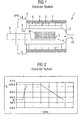
- Figure 1 shows a simplified sectional view of a horizontal Diffusion furnace or a diffusion device 1, with such as such doping of semiconductor bodies can be carried out.
- the horizontal diffusion furnace 1 consists of an SiC (silicon carbide) or quartz glass tube 2 with one Inlet opening for admitting process gas PG and an outlet opening to release used process gas VPG.
- a preferably automatic entry device 3 which is a so-called paddle 4 for holding individual Booting 5, the semiconductor body and preferably Semiconductor wafer W standing upright in the quartz glass tube 2 retracted and extended.
- the diffusion furnace 1 For setting the temperatures required for doping the diffusion furnace 1 also has temperature ranges Heating elements 6, for example, radially around the quartz glass tube 2 are arranged at a predetermined distance. to Thermal insulation of the heating elements 6 and the interior the diffusion furnace 1 or the quartz glass tube 2 is in Thermal insulation 7 is provided outside. Further is in the area of the outlet opening of the quartz glass tube 2 Suction device 8 is provided in the form of a through-flow chamber, whereby the used process gases are sucked off VPG can be.
- a process computer controls one Heating power of the heating elements 6 in their respective zones, a volume flow and a composition of the process gas PG and the automatic entry device 3.
- FIG. 2 shows a simplified graphical representation of a temperature profile according to the prior art, as can be set in the diffusion furnace 1 shown in FIG. 1 to implement doping of the semiconductor wafers W.
- a standby temperature range T B which is, for example, 800 ° C.
- T D a diffusion temperature range
- a doping is carried out on the semiconductor wafer, impurities or dopants being introduced into the interior of the semiconductor body.
- the temperature of the diffusion furnace 1 is again lowered to the standby temperature range T B.
- Figure 3 shows a simplified tabular representation for Illustration of the essential process parameters according to this conventional method.
- the diffusion furnace 1 is initially in a standby state, a standby temperature range T B having a temperature of approximately 800 ° C. and only nitrogen or N 2 being supplied as process gas PG with a gas flow of 15000 ccm / min. 3, for example for about 10 minutes in the standby temperature range, the quartz glass tube 2 is flooded with approximately 50,000 ccm / min N 2 as the carrier gas and then the automatic retraction device 3 is used on the boats 5 placed semiconductor wafers W moved out of the quartz glass tube 2 within 6 minutes.
- a standby temperature range T B having a temperature of approximately 800 ° C. and only nitrogen or N 2 being supplied as process gas PG with a gas flow of 15000 ccm / min. 3
- the quartz glass tube 2 is flooded with approximately 50,000 ccm / min N 2 as the carrier gas and then the automatic retraction device 3 is used on the boats 5 placed semiconductor wafers W moved out of the quartz glass tube 2 within 6 minutes.
- the temperature of the diffusion furnace 1 is now increased (ramped) at a rate of 8.0 ° C. per minute to the diffusion temperature range T D or to a temperature of approx. 1083 ° C.
- the gas flow of the carrier gas N 2 is reduced to 35000 ccm / min and oxygen or O 2 with, for example, 467 ccm / min as reaction gas to form an oxide layer on the surface of the semiconductor wafers fed.
- the oxide layer serves as the starting layer for realizing a dopant source.
- the semiconductor wafers W to be doped are now covered with a dopant, the oxide layer formed during the ramping essentially being further developed and at the same time being provided with dopants or impurities.
- the gas flow of the carrier gas N 2 is usually further reduced to 32000 ccm / min and the gas flow of the reaction gas O 2 is increased to 600 ccm / min, with the process gas PG additionally being supplied with 230 mg as a dopant BBr 3 .
- the temperature of the diffusion furnace 1 is now lowered or oppositely ramped to the standby temperature range T B , for example a rate of -2.0 ° C./min with the carrier gas flow unchanged becomes.
- the standby state is again reached, in which the gas flow of the carrier gas N 2 is reduced again to 15000 ccm / min. In this way, doping can be carried out in the silicon semiconductor wafers W.
- FIG. 4 shows a simplified representation of a dopant concentration distribution D depending on one Location x on the semiconductor wafer W.
- the invention is therefore based on the object of a method to create doping of semiconductor bodies, in which with minimal cost of a dopant concentration distribution in the Semiconductor body equalized and thus a yield is essential is improved.
- a dopant concentration distribution can be in or above the second temperature range in the semiconductor body depending from a particular place much more even be, which causes scatter of process engineering and exploitation-relevant electrical parameters can be reduced and there is an increased yield.
- the first temperature range is preferably around a temperature difference of at least 50 ° C and preferably of approx. Set 200 ° C below the second temperature range, which results in a maximum homogenization of the dopant concentration distribution with minimally increased process time results.
- the first temperature range is preferably greater than 850 ° C. and preferably at about 900 ° C during the second temperature range in a range of 900 to 1100 ° C and preferably is set at about 1100 ° C, which makes it particularly optimal when using silicon semiconductor material Distribution of the dopants over the semiconductor body receives.
- FIG 5 shows a simplified graphic representation of a Temperature profile in the method according to the invention, wherein essentially a diffusion device or a horizontal one Diffusion furnace is used, as described in Figure 1 has been. On a repeated description of this Diffusion device or this diffusion furnace 1 is therefore subsequently waived.
- the temperature profile according to the invention according to FIG. 5 is a two-stage process, the semiconductor bodies initially being set at a first temperature range T I which is lower by a temperature difference of at least 50 ° C. below a final second temperature range T II or brought to be exposed there to the doping gas.
- Figure 6 shows a table of essentials Method steps based on a preferred exemplary embodiment, the same terms or abbreviations being the same or have corresponding meanings as in FIG. 3 and on a repeated description is omitted below.
- silicon semiconductor wafers W in one horizontal diffusion furnace according to Figure 1 doped for example, silicon semiconductor wafers W in one horizontal diffusion furnace according to Figure 1 doped.
- a standby temperature range T B is approximately 800 ° C. and a gas flow of the N 2 carrier gas used is 15000 ccm / min.
- the quartz glass tube 2 can first be flooded with the N 2 carrier gas for about 10 minutes at a temperature of 800 ° C., with a gas flow of the carrier gas about 50000 ccm / min is. After this flooding, the semiconductor wafers W that have already been doped, for example, can be moved out of the diffusion furnace or the quartz glass tube 2 by means of the automatic drive-in device, the process parameters with regard to the temperature and the N 2 carrier gas flow remaining unchanged. This takes about 6 minutes.
- a ramp I or an increase in the temperature of the diffusion furnace 1 up to a first temperature range T I is now a ramp I or an increase in the temperature of the diffusion furnace 1 up to a first temperature range T I.
- the temperature is increased in this step, for example, at a rate of approximately 8.0 ° C./min and, according to FIG. 6, at a rate of 7.8 degrees Celsius / min.
- the gas flow of the N 2 carrier gas is reduced to approximately 35,000 ccm / min, the first temperature range T I being approximately 900 ° C.
- auxiliary layers can be formed on the surface of the semiconductor body or wafer W by means of additional reaction gases in order to improve the doping process.
- an O 2 reaction gas is accordingly supplied to the N 2 carrier gas, as a result of which the process gas PG now also has an oxidizing effect on the semiconductor material.
- a thin silicon dioxide layer is already thermally formed on the surface of the semiconductor wafers during the raising of the temperature to the first temperature range T I and the stabilization step, which layer can be used as a dopant source auxiliary layer in later process steps.
- a first assignment step I in order to cover the semiconductor bodies to be doped with a dopant such as boron in the first temperature range T I, approximately 230 mg BBr 3 is now supplied to the process gas, which contains approximately 32000 ccm / min N 2 and 600 ccm / min O 2 has.
- this coating step I which lasts about 20 minutes, a so-called pre-doping takes place, the dopants, ie boron, in particular being embedded in the oxide layer in particular when using the dopant source auxiliary layer, while the semiconductor body remains essentially undoped.
- phosphorus can also be used as a dopant, the oxide layer acting as a diffusion barrier due to its segregation behavior.
- the diffusion of the dopant can also be made more uniform.
- the formation of this dopant source auxiliary layer can also be omitted, the coating or introduction of the dopants initially taking place only on the surface of the semiconductor body W.
- the first temperature range T I is set at least 50 ° C. and preferably approx. 200 ° C. below the second temperature range T II , a very small dopant concentration distribution, which is very uniform over a location of the semiconductor wafer W, is initially obtained according to FIG. 8 D.
- a new ramp II or an increase in the temperature of the diffusion furnace 1 up to the second temperature range T II is again carried out under a non-doping gas atmosphere, a rate of approximately 8.0 ° C./min being used.
- the second temperature range T II is now approximately 1083 ° C., the gas flow for the carrier gas in turn being increased to 35000 ccm / min and the gas flow of the optionally used reaction gas O 2 being reduced to 467 ccm / min.
- the optionally used dopant source auxiliary layer can be further developed.
- the semiconductor body W to be doped or the auxiliary dopant source layer is then covered with the dopant II in the second temperature range T II . More specifically, 230 mg BBr 3 is again fed to the process gas PG for a period of about 18.5 minutes, the N 2 carrier gas being reduced to 32000 ccm / min and the O 2 reaction gas being increased to 600 ccm / min. As a result, the semiconductor body to be doped is further covered with the dopant, and in particular the auxiliary layer is covered.
- the actual driving of the impurities into the interior of the semiconductor body or wafer W is again preferably in the second temperature range T II (ie at approximately 1083 ° C.), but the reaction gas O 2 (ie at approximately 1083 °) C), however, the reaction gas O 2 and the dopants are removed from the process gas and this only has the carrier gas with a gas flow of 35000 ccm / min. Basically, driving can also take place at even higher temperatures.
- Figure 8 shows an increased dopant concentration distribution D over a location of the semiconductor wafer W after a document II compared to the conventional dopant concentration distribution especially towards the center of the semiconductor wafer W is much more even.
- This more uniform dopant concentration can in the above described driving-in step now also into the interior of the semiconductor body are transmitted, whereby much more even dopant concentrations result for the interior of the semiconductor body and thus a Scattering of process-related and exploitation-relevant electrical Parameters reduced and a yield significantly is increased.
- the temperature of the diffusion furnace 1 is ramped or lowered again to the standby temperature range T B , ie to approximately 800 ° C., preferably a rate of -2.0 ° C./ min and a carrier gas flow of 35000 ccm / min is used. Then, the carrier gas flow can be lowered to the standby state again, wherein about 15,000 cc / min N 2 flow through the quartz glass tube. 2
- Figure 7 shows a simplified graphic representation of a Dopant concentration distribution D as a function of a location x of a semiconductor wafer W to be doped, where after performing the doping method according to the invention substantially uniform dopant concentration distribution can be realized.
- an approximately 600 nm thick oxide layer is formed as a dopant auxiliary layer in the process described above, the formation of this layer can also be omitted and only a preliminary doping in a first temperature range T I and a final doping in a second temperature range T II can be carried out.
- any other semiconductor material can also be used.
- reaction gas O 2 reaction gas
- dopant material BBr 3 dopant material
- other carrier gas, reaction gas and / or dopant materials can of course also be used to implement a corresponding p and / or n doping.
- the extent of the improvement in the dopant concentration distribution increases with a temperature difference between the first temperature range T I and the second temperature range T II .
- the temperature of the first temperature range T I cannot be reduced as far as desired, since the reaction speed also decreases as the temperature drops, and the extent of the essential predoping is thus limited.
- the gas flow of the process gas takes on a usually non-uniform distribution of the dopant in the quartz glass tube 2, while at higher temperatures the dopant is distributed even better due to its entropy.
- the empirically determined limit value for the first temperature range T I is therefore above 850 ° C. and preferably around 900 ° C.
Landscapes
- Crystals, And After-Treatments Of Crystals (AREA)
Abstract
Description
Claims (16)
- Verfahren zum Dotieren von Halbleiterkörpern mit den Schritten:a) Vorbereiten einer Diffusionseinrichtung (1) in einem Bereitschafts-Temperaturbereich (TB);b) Einfahren von zu dotierenden Halbleiterkörpern (W) in die Diffusionseinrichtung (1);c) Erhöhen einer Temperatur der Diffusionseinrichtung (1) bis zu einem ersten Temperaturbereich (TI);d) Belegen der zu dotierenden Halbleiterkörper (W) mit einem Dotierstoff im ersten Temperaturbereich (TI);e) Erhöhen einer Temperatur der Diffusionseinrichtung (1) bis zu einem zweiten Temperaturbereich (TII);f) Belegen der zu dotierenden Halbleiterkörper (W) mit dem Dotierstoff im zweiten Temperaturbereich (TII);g) Eintreiben des Dotierstoffes in das Innere der Halbleiterkörper (W) im oder oberhalb des zweiten Temperaturbereichs (TII) ; undh) Erniedrigen einer Temperatur der Diffusionseinrichtung (1) bis zum Bereitschafts-Temperaturbereich (TB).
- Verfahren nach Patentanspruch 1,
dadurch gekennzeichnet, dass der erste Temperaturbereich (TI) um eine Temperaturdifferenz von mindestens 50 °C und vorzugsweise von ca. 200 °C unterhalb des zweiten Temperaturbereichs (TII) eingestellt wird. - Verfahren nach Patentanspruch 1 oder 2,
dadurch gekennzeichnet, dass der erste Temperaturbereich (TI) größer 850 °C und vorzugsweise bei ca. 900 °C eingestellt wird. - Verfahren nach einem der Patentansprüche 1 bis 3,
dadurch gekennzeichnet, dass der zweite Temperaturbereich (TII) in einem Bereich von 900 bis 1100 °C und vorzugsweise bei ca. 1083 °C eingestellt wird. - Verfahren nach einem der Patentansprüche 1 bis 4,
dadurch gekennzeichnet, dass der Bereitschafts-Temperaturbereich (TB) unterhalb von 850 °C und vorzugsweise bei ca. 800 °C eingestellt wird. - Verfahren nach einem der Patentansprüche 1 bis 5,
dadurch gekennzeichnet, dass beim Erhöhen der Temperatur in Schritt e) und/oder beim Belegen in Schritt f) eine Oxidation einer Oberfläche der Halbleiterkörper (W) in der Diffusionseinrichtung (1) durchgeführt wird. - Verfahren nach einem der Patentansprüche 1 bis 6,
dadurch gekennzeichnet, dass das Dotieren der Halbleiterkörper (W) aus der Gasphase mittels eines Prozessgases (PG) erfolgt. - Verfahren nach einem der Patentansprüche 1 bis 7,
dadurch gekennzeichnet, dass als Diffusionseinrichtung (1) ein horizontaler Diffusionsofen verwendet wird. - Verfahren nach einem der Patentansprüche 1 bis 8,
dadurch gekennzeichnet, dass als Halbleiterkörper (W) Silizium-Halbleiterwafer verwendet werden. - Verfahren nach einem der Patentansprüche 7 bis 9,
dadurch gekennzeichnet, dass als Prozessgas ein Trägergas, ein Reaktionsgas und/oder ein Dotiergas verwendet wird. - Verfahren nach einem der Patentansprüche 1 bis 10,
dadurch gekennzeichnet, dass das Erhöhen der Temperatur in den Schritten c) und e) mit einer Rate von ca. 8,0 °C/Minute durchgeführt wird. - Verfahren nach einem der Patentansprüche 1 bis 11,
dadurch gekennzeichnet, dass nach dem Erhöhen der Temperatur in Schritt c) eine Stabilisierung des ersten Temperaturbereichs (TI) durchgeführt wird. - Verfahren nach einem der Patentansprüche 1 bis 12,
dadurch gekennzeichnet, dass das Belegen in den Schritten d) und f) für ca. 20 Minuten durchgeführt wird. - Verfahren nach einem der Patentansprüche 1 bis 13,
dadurch gekennzeichnet, dass das Eintreiben in Schritt g) für ca. 60 Minuten durchgeführt wird. - Verfahren nach einem der Patentansprüche 1 bis 14,
dadurch gekennzeichnet, dass das Erniedrigen der Temperatur in Schritt h) mit einer Rate von ca. - 2,0 °C/Minute durchgeführt wird. - Verfahren nach einem der Patentansprüche 1 bis 15,
dadurch gekennzeichnet, dass beim Vorbereiten der Diffusionseinrichtung (1) in Schritt a) ein Fluten mit Trägergas und
ein Ausfahren von bereits dotierten Halbleiterkörpern (W) durchgeführt wird.
Applications Claiming Priority (2)
| Application Number | Priority Date | Filing Date | Title |
|---|---|---|---|
| DE10301244 | 2003-01-15 | ||
| DE10301244A DE10301244B4 (de) | 2003-01-15 | 2003-01-15 | Verfahren zum Dotieren von Halbleiterkörpern |
Publications (2)
| Publication Number | Publication Date |
|---|---|
| EP1439573A2 true EP1439573A2 (de) | 2004-07-21 |
| EP1439573A3 EP1439573A3 (de) | 2007-01-03 |
Family
ID=32519974
Family Applications (1)
| Application Number | Title | Priority Date | Filing Date |
|---|---|---|---|
| EP03030033A Withdrawn EP1439573A3 (de) | 2003-01-15 | 2003-12-31 | Verfahren zum Dotieren von Halbleiterkörpern |
Country Status (2)
| Country | Link |
|---|---|
| EP (1) | EP1439573A3 (de) |
| DE (1) | DE10301244B4 (de) |
Families Citing this family (1)
| Publication number | Priority date | Publication date | Assignee | Title |
|---|---|---|---|---|
| DE102012207764B4 (de) | 2012-05-09 | 2022-08-11 | International Solar Energy Research Center Konstanz E.V. | Verfahren zur Bor-Dotierung von Silizium-Wafern |
Family Cites Families (4)
| Publication number | Priority date | Publication date | Assignee | Title |
|---|---|---|---|---|
| JP2928930B2 (ja) * | 1989-12-06 | 1999-08-03 | セイコーインスツルメンツ株式会社 | 不純物ドーピング装置 |
| JPH0758698B2 (ja) * | 1990-08-22 | 1995-06-21 | 信越半導体株式会社 | 半導体ウエーハヘのボロン拡散方法 |
| JP4022997B2 (ja) * | 1998-07-29 | 2007-12-19 | 住友電気工業株式会社 | 3−5族化合物半導体結晶へのZn拡散方法及び拡散装置 |
| JP4655321B2 (ja) * | 1999-08-27 | 2011-03-23 | 東京エレクトロン株式会社 | 熱処理方法 |
-
2003
- 2003-01-15 DE DE10301244A patent/DE10301244B4/de not_active Expired - Fee Related
- 2003-12-31 EP EP03030033A patent/EP1439573A3/de not_active Withdrawn
Also Published As
| Publication number | Publication date |
|---|---|
| EP1439573A3 (de) | 2007-01-03 |
| DE10301244A1 (de) | 2004-08-05 |
| DE10301244B4 (de) | 2005-03-17 |
Similar Documents
| Publication | Publication Date | Title |
|---|---|---|
| DE69915729T2 (de) | Stickstoffdotierte einkristalline Siliziumscheibe mit geringen Fehlstellen und Verfahren zu ihrer Herstellung | |
| DE69713758T2 (de) | Bandgegossener siliciumcarbid-ersatzwafer | |
| DE102011002398B4 (de) | Verfahren zum Herstellen einer Siliziumcarbid-Halbleitervorrichtung | |
| DE19611043B4 (de) | Verfahren zum Herstellen eines Siliciumwafers, Verfahren zum Bilden eines Siliciumwafers und Verfahren zur Herstellung eines Halbleiterbauelements | |
| DE3123231C2 (de) | ||
| DE102017217540B4 (de) | Herstellungsverfahren für einkristallines Silicium und einkristallines Silicium | |
| EP0018520A1 (de) | Verfahren zur vollständigen Ausheilung von Gitterdefekten in durch Ionenimplantation von Phosphor erzeugten N-leitenden Zonen einer Siliciumhalbleitervorrichtung und zugehörige Siliciumhalbleitervorrichtung | |
| DE112012002217B4 (de) | Verfahren zur Herstellung eines GaAs-Einkristalls und GaAs-Einkristallwafer | |
| DE102008022502B4 (de) | Verfahren zum Herstellen eines Halbleiterelements in einem Substrat | |
| DE102008046617A1 (de) | Halbleiterscheibe aus einkristallinem Silizium und Verfahren für deren Herstellung | |
| DE4438398C2 (de) | Wärmebehandlungsverfahren für Verbindungshalbleiter und Verwendung eines Suszeptors in der Wärmebehandlung | |
| DE112016002091B4 (de) | Silicium-Epitaxie-Wafer und Verfahren zu dessen Herstellung | |
| EP0048288A1 (de) | Verfahren zur Dotierung von Halbleiterbauelementen mittels Ionenimplantation | |
| DE2334258A1 (de) | Verfahren zum dotieren von halbleitermaterialien | |
| DE102008039058A1 (de) | Halbleiterwafer für Halbleiterbauelemente und Verfahren zur Herstellung derselben | |
| EP1439573A2 (de) | Verfahren zum Dotieren von Halbleiterkörpern | |
| WO2001088974A1 (de) | Einstellung von defektprofilen in kristallen oder kristallähnlichen strukturen | |
| DE60108078T2 (de) | Heizungsanlage und Verfahren zur Heizung für einen Reaktor | |
| DE19633184B4 (de) | Verfahren zur Herstellung eines Halbleiterbauelements mit durch Ionenimplantation eingebrachten Fremdatomen | |
| EP3464688B1 (de) | Verfahren zur herstellung einer halbleiterscheibe aus einkristallinem silizium und vorrichtung zur herstellung einer halbleiterscheibe aus einkristallinem silizium | |
| DE3424487A1 (de) | Einkristall auf basis von seltenerdmetall-gallium-granat | |
| DE1286644B (de) | Verfahren zum Ausdiffundieren dotierender Fremdstoffe aus einem Halbleiterkoerper | |
| DE112023004074T5 (de) | Verfahren zur züchtung eines einkristalls, verfahren zur herstellung eines halbleitersubstrats und halbleitersubstrat | |
| DE112017005180T5 (de) | Verfahren zum Auflösen eines vergrabenen Oxids in einem Silicon-On-Insulator-Wafer | |
| WO2000039840A1 (de) | Verfahren zur bor-dotierung von wafern unter einsatz eines vertikalofensystems |
Legal Events
| Date | Code | Title | Description |
|---|---|---|---|
| PUAI | Public reference made under article 153(3) epc to a published international application that has entered the european phase |
Free format text: ORIGINAL CODE: 0009012 |
|
| AK | Designated contracting states |
Kind code of ref document: A2 Designated state(s): AT BE BG CH CY CZ DE DK EE ES FI FR GB GR HU IE IT LI LU MC NL PT RO SE SI SK TR |
|
| AX | Request for extension of the european patent |
Extension state: AL LT LV MK |
|
| PUAL | Search report despatched |
Free format text: ORIGINAL CODE: 0009013 |
|
| AK | Designated contracting states |
Kind code of ref document: A3 Designated state(s): AT BE BG CH CY CZ DE DK EE ES FI FR GB GR HU IE IT LI LU MC NL PT RO SE SI SK TR |
|
| AX | Request for extension of the european patent |
Extension state: AL LT LV MK |
|
| RIC1 | Information provided on ipc code assigned before grant |
Ipc: H01L 21/225 20060101ALI20061127BHEP Ipc: H01L 21/223 20060101AFI20061127BHEP |
|
| AKX | Designation fees paid | ||
| STAA | Information on the status of an ep patent application or granted ep patent |
Free format text: STATUS: THE APPLICATION IS DEEMED TO BE WITHDRAWN |
|
| 18D | Application deemed to be withdrawn |
Effective date: 20070704 |
|
| REG | Reference to a national code |
Ref country code: DE Ref legal event code: 8566 |