EP1437638A1 - Schaltung zur Erzeugung einer Versorgungsspannung - Google Patents
Schaltung zur Erzeugung einer Versorgungsspannung Download PDFInfo
- Publication number
- EP1437638A1 EP1437638A1 EP20020028082 EP02028082A EP1437638A1 EP 1437638 A1 EP1437638 A1 EP 1437638A1 EP 20020028082 EP20020028082 EP 20020028082 EP 02028082 A EP02028082 A EP 02028082A EP 1437638 A1 EP1437638 A1 EP 1437638A1
- Authority
- EP
- European Patent Office
- Prior art keywords
- voltage
- noise
- output
- supply voltage
- low
- Prior art date
- Legal status (The legal status is an assumption and is not a legal conclusion. Google has not performed a legal analysis and makes no representation as to the accuracy of the status listed.)
- Granted
Links
- 230000001105 regulatory effect Effects 0.000 claims description 8
- 238000011144 upstream manufacturing Methods 0.000 claims description 2
- 230000009467 reduction Effects 0.000 description 4
- 238000011161 development Methods 0.000 description 3
- 230000018109 developmental process Effects 0.000 description 3
- 230000008901 benefit Effects 0.000 description 2
- 230000008859 change Effects 0.000 description 2
- 230000007423 decrease Effects 0.000 description 2
- 230000001419 dependent effect Effects 0.000 description 2
- 238000000034 method Methods 0.000 description 2
- 230000008569 process Effects 0.000 description 2
- 230000005611 electricity Effects 0.000 description 1
- 230000004044 response Effects 0.000 description 1
- 230000001629 suppression Effects 0.000 description 1
Images

Classifications
-
- G—PHYSICS
- G05—CONTROLLING; REGULATING
- G05F—SYSTEMS FOR REGULATING ELECTRIC OR MAGNETIC VARIABLES
- G05F1/00—Automatic systems in which deviations of an electric quantity from one or more predetermined values are detected at the output of the system and fed back to a device within the system to restore the detected quantity to its predetermined value or values, i.e. retroactive systems
- G05F1/10—Regulating voltage or current
- G05F1/46—Regulating voltage or current wherein the variable actually regulated by the final control device is DC
- G05F1/56—Regulating voltage or current wherein the variable actually regulated by the final control device is DC using semiconductor devices in series with the load as final control devices
- G05F1/565—Regulating voltage or current wherein the variable actually regulated by the final control device is DC using semiconductor devices in series with the load as final control devices sensing a condition of the system or its load in addition to means responsive to deviations in the output of the system, e.g. current, voltage, power factor
- G05F1/569—Regulating voltage or current wherein the variable actually regulated by the final control device is DC using semiconductor devices in series with the load as final control devices sensing a condition of the system or its load in addition to means responsive to deviations in the output of the system, e.g. current, voltage, power factor for protection
Definitions
- the invention relates to a circuit for generating a Supply voltage, which for example for power supply of a chip can serve.
- Some chips require that an external External supply voltage generated by the voltage source must first be regulated and then for the Chip core can be used.
- the necessary ones Voltage regulators require a reference voltage, which in the Usually generated in the chip itself.
- Two can Noise paths occur.
- the first noise path concerns the path from the external voltage source to the reference voltage source and from the reference voltage source to the voltage supply for the chip core.
- the second noise path concerns the path from the external voltage source for the power supply for the Chip core. Consideration of the noise paths is particularly important important because the reference voltage regulator, which generates the reference voltage, usually a worse one Has noise reduction than the supply voltage regulator in the chip core. If the noise in the reference voltage source is too high, it may even be be destroyed.
- a circuit for generating is from the prior art a supply voltage as shown in FIG. 1, known.
- a voltage regulator 1 that has no special precautions for noise reduction is on the input side connected to a voltage input IN at which an external Supply voltage EXTVDD is present.
- the voltage regulator 1 generates a reference supply voltage at its output REFVDD, which is led to a reference voltage source 2.
- the reference voltage source 2 generates a reference voltage therefrom VREF, which is then a low-noise voltage regulator 3 is fed via its first input 3.1.
- At the second input 3.2 of the low-noise voltage regulator 3 is the external supply voltage applied to the voltage input IN EXTVDD on.
- the low-noise voltage regulator 3 generates then a supply voltage VDD, which at the output 3.4 of the low-noise voltage regulator 3 can be tapped. If the low-noise voltage regulator 3 additionally a regulated voltage supply needed, this can be used as a reference supply voltage REFVDD provided via input 3.3 be what is indicated in Figure 1 by the dotted line is.
- FIG. 1 for a power supply has the disadvantage that suppresses the noise of the reference voltage supply only to a limited extent becomes, which leads to the supply voltage VDD at the output of the circuit may be noisy.
- circuit for the power supply for the The chip core therefore has only limited noise suppression on.
- FIG. 2 Embodiment of a circuit for generating a supply voltage shown.
- the external supply voltage EXTVDD created.
- the circuit in Figure 2 differs of the circuit shown in Figure 1 in that the in Figure 1 used noisy voltage regulator 1 by a low-noise voltage regulator 6 and a simple reference voltage regulator 4, which has no special noise reduction has been replaced.
- the second is low-noise voltage regulator 6 via its input 6.2 with the Voltage input IN connected.
- the external supply voltage EXTVDD becomes a first one Reference voltage VREF1 formed at the input 6.1 of the low-noise voltage regulator 6 is present.
- the reference voltage REFVDD with the low-noise second voltage regulator 6 generated.
- this embodiment has the following Disadvantage.
- the additional second low-noise voltage regulator 6 needs more space on the chip.
- An object of the invention is to provide a circuit for generation specify a supply voltage at which, on the one hand the noise component in the supply voltage is as low as is possible and on the other hand the necessary for the circuit Area is also minimized.
- the task is accomplished by a circuit for generating a Supply voltage with the features according to claim 1 solved.
- the circuit according to the invention for generating a supply voltage has a voltage input, which with a voltage regulator for generating a first supply voltage and a low-noise voltage regulator for generation is connected to a low-noise supply voltage. additionally a control unit is provided, by means of which it can be determined is which of the two supply voltages on one Supply voltage output of the circuit switched becomes.
- a first is controllable Switch provided via which the voltage regulator with the supply voltage output is connectable.
- a second controllable switch is provided, via which the low-noise voltage regulator with the supply voltage output is connectable.
- the two are on the control unit controllable switch controllable.
- the circuit according to the invention is advantageous the first and second controllable switches as transistors educated.
- control unit has a first Control output and a second control output, the second control output by inverting the first control output is formed.
- Control unit be designed so that depending on the low-noise supply voltage one of the two supply voltages to the supply voltage output of the circuit is switched. This ensures that based on certain Criteria resulting from the low-noise supply voltage derived, it is determined when between the first supply voltage and the low-noise supply voltage is switched.
- control unit can be designed so that depending on one Reference voltage one of the two supply voltages switched to the supply voltage output of the circuit becomes. That is, only when the reference voltage is determined Criteria met, is from the first supply voltage the low-noise supply voltage switched.
- Control unit be designed so that depending on the Voltage input applied supply voltage one of the two supply voltages on the supply voltage output the circuit is switched. So the time the switchover from the first supply voltage to the low-noise supply voltage based on certain criteria, which result from the external supply voltage.
- the Circuit according to the invention a unit for generating the reference voltage which the low-noise voltage regulator is connected upstream.
- the low noise voltage regulator an input for a regulated Supply voltage on which can be controlled via the first Switch with the output of the low-noise voltage regulator connected is.
- the voltage regulator has a P-channel MOS transistor. With which can help the supply voltage during the switch-on phase be made available quickly.
- Circuit of low noise voltage regulator an N-channel MOS transistor exhibit. So that at the output of the circuit low-noise supply voltage can be made available.
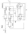
- Circuit for generating a supply voltage becomes an external supply voltage at the voltage input IN EXTVDD created on the one hand at input 1.1 of a Voltage amplifier 1 and at the input 3.1 of a low-noise voltage amplifier 3 is present.
- the voltage amplifier 1 is on the output side, i.e. via its output 1.2, via a controllable switch SWNOISY with the output O connected to the circuit.
- the output 3.4 of the low noise Voltage amplifier 3 is controllable via another SWQUIET switch also with output O of the circuit connected.
- the reference supply voltage is at the output O of the circuit REFVDD can be tapped, which is either the same as the NOISYVDD or noise compensated supply voltage the low-noise supply voltage is VDD.
- the two controllable SWNOISY and SWQUIET switches are on the two Control voltages SWNOISYVDD or SWVDD, which from a Control unit SE originate, controlled.
- the control unit SE generates the two control voltages SWVDD and SWNOISYVDD depending from that generated by the low noise voltage regulator 3 Supply voltage VDD, which is connected to input 7.3 a decision unit 7 is performed, depending from a reference voltage VREF, which is connected to input 7.1 of the decision maker 7 and is dependent on the external voltage EXTVDD, which is connected to input 7.2 of the decision maker 7 is performed.
- the control voltage is SWNOISYVDD can be tapped at the output 9.3 of an inverter INV and forms that inverted signal to the input 9.1 of the inverter INV Signal with the voltage SWVDD.
- a reference voltage source 2 With the help of a reference voltage source 2 becomes the reference supply voltage REFVDD the reference voltage VREF formed and on the Input 3.2 of the low-noise voltage regulator 3 out.
- the low-noise voltage regulator 3 is an additional regulated one Supply voltage required for operation is the Input 3.3 is provided on the low-noise voltage regulator 3, which if necessary, what is represented by the dotted line is connectable to the reference voltage REFVDD.
- the decision unit When switched on, the decision unit generates 7, also referred to as a switch-on detector its output 7.4 is a control signal with the control voltage SWVDD, which is equal to the external supply voltage EXTVDD is. A control voltage is then present at the output 9.3 of the inverter INV SWNOISYVDD, which is zero.
- the Switch SWQUIET is due to the control voltage SWVDD, which forms the control voltage for the SWQUIET switch switched off, that is not conductive.
- the reference supply voltage REFVDD is not equal to that noise compensated voltage NOISYVDD, which at the output 1.2 of the Voltage regulator 1 is present. Because the external supply voltage EXTVDD is high, it is not noise compensated Voltage NOISYVDD from zero to a certain one regulated value increase. During this time, i.e. the switch-on time, is the non-noise compensated voltage NOISYVDD is the reference supply voltage REFVDD of the circuit for power supply. At the output of the reference voltage source 2, the reference voltage VREF also increases in value Zero to the value of the reference voltage.
- the low noise Voltage regulator 3 is then able to control the low-noise voltage Regulate VDD correctly, so that the low-noise voltage VDD at output 3.4 of the low-noise voltage regulator 3 from Value zero increases to the regulated value.
- the switch-on detector 7 switches the voltage SWVDD to the value zero via its output 7.4, so that the controllable switch SWQUIET becomes conductive. Because now the SWNOISYVDD signal is equal to the external supply voltage Is EXTVDD, the controllable switch SWNOISY is not in the brought conductive state.
- the reference voltage source 2 is now supplied via the low-noise voltage regulator 3 and the low noise voltage regulator 3 uses that from the reference voltage source 2 generated reference voltage VREF.
- the control voltage SWVDD is on Output 7.4 of the switch-on detector 7 is equal to the external supply voltage EXTVDD.
- the voltage SWVDD at output 7.4 drops to the value Zero down.
- you can different criteria are used. You can for example a time constant, the level of voltage VDD or the level of the voltage difference between the two Voltages be VDD and VREF.
- the two controllable switches SWNOISY and SWQUIET are preferred trained as transistors and work on the same way. The following is how it works of the controllable switch SWQUIET.
- the controllable switch SWQUIET is conductive when the control voltage SWVDD less than the difference between the voltages VDD - Vt or the control voltage SWVDD is less than is the difference between the voltages REFVDD - Vt.
- the voltage REFVDD at the output of the controllable SWQUIET switch is equal to the voltage VDD. If the Control voltage SWVDD is greater than the difference between VDD - Vt and greater than the difference between REFVDD - Vt the controllable switch SWQUIET is not conductive and the two voltages VDD and REFVDD are independent of one another.
- the voltage Vt is a constant voltage.
- the inverter INV also generates a signal at its output 9.3 the voltage SWNOISYVDD is zero when the voltage SWVDD at its input 9.1 equal to the supply voltage EXTVDD is. If the voltage at input 9.1 of the inverter INV is equal to zero, the inverter INV generates a voltage SWNOISYVDD, which is equal to the external supply voltage EXTVDD is.
- the voltage amplifier 1 shown in FIG. 4 P-channel MOS transistor shown are used. in principle has a PMOS voltage regulator inherently an unfavorable PSRR (Power Supply Rejection Ratio). Based on the following This can be seen, for example. If the voltage at the input IN1 drops very quickly by one volt, the gate voltage must reduce the PMOS gate voltage very quickly by one volt, to keep the output voltage at output OUT1 constant hold. However, since the circuit first reduced with a certain delay is the change by one volt at the IN1 input, at least partially at the output OUT1. Therefore, always turns on at output OUT1 certain noise can be seen. The PMOS controller points also bad response behavior in the event of a change the load at output OUT1.
- PSRR Power Supply Rejection Ratio
- the regulator circuit needs the gate voltage to reduce.
- the PMOS transistor 10 also reacts here only after a certain amount of time, which leads to that the voltage at output OUT1 drops while the gate voltage still remains constant.
- the gate-source voltage decreases, which leads to the output voltage at the output OUT 1 continues to decrease. Because of these properties, the PMOS voltage regulator suitable for voltage regulator 1.
- the N-channel MOS transistor 11 shown in FIG. 5 can be used for the circuit according to the invention for the low-noise voltage regulator 3 can be used.
- the NMOS transistor 11 has the advantage that it has a good PSRR.
- the NMOS gate voltage must be kept constant to keep the voltage at output OUT2 constant, which is also achieved by the NMOS voltage regulator.
- the NMOS controllers also have better behavior with regard to load changes at output OUT2 than this for the one shown in FIG PMOS transistor is the case.
- the load on Output OUT2 increases very quickly while the voltage at Input IN2 remains constant, then the controller circuit increase the gate voltage to the voltage at output OUT2 to keep constant.
- the voltage regulator only after reacts for a certain period of time, the voltage at the output drops OUT2 while the gate voltage remains constant.
- the gate-source voltage UGS is increasing, which has the consequence that the Ringing of the voltage at output OUT2 is limited.
- the PMOS transistor shown in Figure 4 is significantly simpler to implement on a chip and the cost is significantly lower than in the NMOS transistor shown in FIG. 5.
- the gate voltage remains with a PMOS transistor between the voltage present at input IN1 and Zero volts. With an NMOS transistor, the gate voltage exceed the voltage at input IN2 so that a charge pump is required.
Landscapes
- Engineering & Computer Science (AREA)
- Physics & Mathematics (AREA)
- Electromagnetism (AREA)
- General Physics & Mathematics (AREA)
- Radar, Positioning & Navigation (AREA)
- Automation & Control Theory (AREA)
- Continuous-Control Power Sources That Use Transistors (AREA)
Abstract
Description
- Figur 1
- zeigt eine Schaltung zur Erzeugung einer Versorgungsspannung gemäß dem Stand der Technik.
- Figur 2
- zeigt eine zweite Ausführungsform einer Schaltung zur Erzeugung einer Versorgungsspannung gemäß dem Stand der Technik.
- Figur 3
- zeigt eine Schaltung zur Erzeugung einer Versorgungsspannung gemäß der Erfindung.
- Figur 4
- zeigt eine Ausführungsform für einen Spannungsregler, wie er bei der erfindungsgemäßen Schaltung zum Einsatz kommen kann.
- Figur 5
- zeigt eine Ausführungsform für einen rauscharmen Spannungsregler, wie er bei der erfindungsgemäßen Schaltung zum Einsatz kommen kann.
- 1
- Spannungsregler mit beschränkter Rauschunterdrükkung
- 2
- Einheit zur Erzeugung einer Referenzspannung
- 3
- erster rauscharmer Spannungsregler
- 4
- rauschbehaftete Einheit zur Erzeugung einer Referenzspannung
- 6
- zweiter rauscharmer Spannungsregler
- 7
- Einschaltsteuerung
- 7.1
- erster Eingang der Einschaltsteuerung
- 7.2
- zweiter Eingang der Einschaltsteuerung
- 7.3
- dritter Eingang der Einschaltsteuerung
- 7.4
- Ausgang der Einschaltsteuerung
- 9.1
- Invertereingang
- 9.2
- Betriebsspannungsanschluss des Inverters
- 9.3
- Inverterausgang
- 10
- PMOS-Transistor
- 11
- NMOS-Transistor
- SE
- Steuereinheit
- EXTVDD
- externe Versorgungsspannung
- REFVDD
- Referenzversorgungsspannung
- VREF
- Referenzspannung
- VREF1
- erste Referenzspannung
- VREF2
- zweite Referenzspannung
- VDD
- Versorgungsspannung
- IN
- Eingang
- O
- Ausgang
- INV
- Inverter
- NOISYVDD
- nicht rauschkompensierte Versorgungsspannung
- SWNOISY
- erster steuerbarer Schalter
- SWQUIET
- zweiter steuerbarer Schalter
- SWNOISYVDD
- erste Steuerspannung
- SWVDD
- zweite Steuerspannung
Claims (11)
- Schaltung zur Erzeugung einer Versorgungsspannung, mit einem Spannungseingang (IN), welcher mit einem Spannungsregler (1) zur Erzeugung einer ersten Versorgungsspannung (NOISYVDD) und mit einem rauscharmen Spannungsregler (3) zur Erzeugung einer rauscharmen Versorgungsspannung (VDD) verbunden ist, und
mit einer Steuereinheit (SE) mittels welcher bestimmbar ist, welche der beiden Versorgungsspannungen (NOISYVDD, VDD) auf einen Versorgungsspannungsausgang (0) der Schaltung geschaltet wird. - Schaltung nach Patentanspruch 1,
mit einem ersten steuerbaren Schalter (SWNOISY), über den der Spannungsregler (1) mit dem Versorgungsspannungsausgang (O) verbindbar ist,
mit einem zweiten steuerbaren Schalter (SWQUIET), über den der rauscharme Spannungsregler (2) mit dem Versorgungsspannungsausgang (0) verbindbar ist, und
wobei die Steuereinheit (SE) die beiden steuerbaren Schalter (SWNOISY, SWQUIET) steuert. - Schaltung nach Patentanspruch 2,
wobei der erste und der zweite steuerbare Schalter (SWNOISY, SWQUIET) als Transistoren ausgebildet sind. - Schaltung nach einem der Patentansprüche 1 bis 3,
wobei die Steuereinheit (SE) einen ersten Steuerausgang (7.4) und einen zweiten Steuerausgang (9.3) aufweist, wobei der zweiten Steuerausgang (9.3) durch eine Invertierung des ersten Steuerausgangs (7.4) gebildet ist. - Schaltung nach einem der Patentansprüche 1 bis 4,
wobei die Steuereinheit (SE) so ausgebildet ist, dass abhängig von der rauscharmen Versorgungsspannung (VDD) eine der beiden Versorgungsspannungen (NOISYVDD, VDD) auf den Versorgungsspannungsausgang (O) der Schaltung geschaltet wird. - Schaltung nach einem der Patentansprüche 1 bis 5,
wobei die Steuereinheit (SE) so ausgebildet ist, dass abhängig von einer Referenzspannung (VREF) eine der beiden Versorgungsspannungen (NOISYVDD, VDD) auf den Versorgungsspannungsausgang (O) der Schaltung geschaltet wird. - Schaltung nach einem der Patentansprüche 1 bis 7,
wobei die Steuereinheit (SE) so ausgebildet ist, dass abhängig von der am Spannungseingang (IN) anliegenden Versorgungsspannung (EXTVDD) eine der beiden Versorgungsspannungen (NOISYVDD, VDD) auf den Versorgungsspannungsausgang (O) der Schaltung geschaltet wird. - Schaltung nach einem der Patentansprüche 6 bis 8,
mit einer Einheit (2) zur Erzeugung der Referenzspannung (VREF), welche dem rauscharmen Spannungsregler (3) vorgeschaltet ist. - Schaltung nach einem der Patentansprüche 1 bis 9,
wobei der rauscharme Spannungsregler (3) einen Eingang (3.3) für eine geregelte Versorgungsspannung (REFVDD) aufweist, welcher über den ersten steuerbaren Schalter (SWQUIET) mit dem Ausgang (3.4) des rauscharmen Spannungsreglers (3) verbunden ist. - Schaltung nach einem der Patentansprüche 1 bis 9,
wobei der Spannungsregler (1) einen P-Kanal MOS Transistor (10) aufweist. - Schaltung nach einem der Patentansprüche 1 bis 10,
wobei der rauscharme Spannungsregler (3) einen N-Kanal MOS Transistor (11) aufweist.
Priority Applications (3)
| Application Number | Priority Date | Filing Date | Title |
|---|---|---|---|
| EP02028082.2A EP1437638B1 (de) | 2002-12-17 | 2002-12-17 | Schaltung zur Erzeugung einer Versorgungsspannung |
| PCT/EP2003/013707 WO2004055613A1 (de) | 2002-12-17 | 2003-12-04 | Schaltung zur erzeugung einer versorgungsspannung |
| US11/155,321 US7405548B2 (en) | 2002-12-17 | 2005-06-16 | Circuit for generating a supply voltage |
Applications Claiming Priority (1)
| Application Number | Priority Date | Filing Date | Title |
|---|---|---|---|
| EP02028082.2A EP1437638B1 (de) | 2002-12-17 | 2002-12-17 | Schaltung zur Erzeugung einer Versorgungsspannung |
Publications (2)
| Publication Number | Publication Date |
|---|---|
| EP1437638A1 true EP1437638A1 (de) | 2004-07-14 |
| EP1437638B1 EP1437638B1 (de) | 2016-02-24 |
Family
ID=32479725
Family Applications (1)
| Application Number | Title | Priority Date | Filing Date |
|---|---|---|---|
| EP02028082.2A Expired - Lifetime EP1437638B1 (de) | 2002-12-17 | 2002-12-17 | Schaltung zur Erzeugung einer Versorgungsspannung |
Country Status (3)
| Country | Link |
|---|---|
| US (1) | US7405548B2 (de) |
| EP (1) | EP1437638B1 (de) |
| WO (1) | WO2004055613A1 (de) |
Families Citing this family (2)
| Publication number | Priority date | Publication date | Assignee | Title |
|---|---|---|---|---|
| US8471414B2 (en) * | 2005-06-24 | 2013-06-25 | The Flewelling Ford Family Trust | Low impedance polarity conversion circuit |
| US11095216B2 (en) | 2014-05-30 | 2021-08-17 | Qualcomm Incorporated | On-chip dual-supply multi-mode CMOS regulators |
Citations (4)
| Publication number | Priority date | Publication date | Assignee | Title |
|---|---|---|---|---|
| EP0260474A1 (de) * | 1986-09-18 | 1988-03-23 | International Business Machines Corporation | Stromversorgungsadaptersystem |
| US5563498A (en) * | 1991-07-17 | 1996-10-08 | Halcro Nominees Pty Ltd. | Power supply regulator |
| US20020043963A1 (en) * | 2001-11-01 | 2002-04-18 | Vipin Malik | Power supply configuration for low-noise applications in limited-energy environments |
| US20020089317A1 (en) * | 2000-11-08 | 2002-07-11 | Stmicroelectronics S.R.I. | Voltage regulator for low-consumption circuits |
Family Cites Families (3)
| Publication number | Priority date | Publication date | Assignee | Title |
|---|---|---|---|---|
| US6583610B2 (en) * | 2001-03-12 | 2003-06-24 | Semtech Corporation | Virtual ripple generation in switch-mode power supplies |
| US6788035B2 (en) * | 2001-06-12 | 2004-09-07 | Primarion, Inc. | Serial bus control method and apparatus for a microelectronic power regulation system |
| US6977492B2 (en) * | 2002-07-10 | 2005-12-20 | Marvell World Trade Ltd. | Output regulator |
-
2002
- 2002-12-17 EP EP02028082.2A patent/EP1437638B1/de not_active Expired - Lifetime
-
2003
- 2003-12-04 WO PCT/EP2003/013707 patent/WO2004055613A1/de not_active Ceased
-
2005
- 2005-06-16 US US11/155,321 patent/US7405548B2/en not_active Expired - Lifetime
Patent Citations (4)
| Publication number | Priority date | Publication date | Assignee | Title |
|---|---|---|---|---|
| EP0260474A1 (de) * | 1986-09-18 | 1988-03-23 | International Business Machines Corporation | Stromversorgungsadaptersystem |
| US5563498A (en) * | 1991-07-17 | 1996-10-08 | Halcro Nominees Pty Ltd. | Power supply regulator |
| US20020089317A1 (en) * | 2000-11-08 | 2002-07-11 | Stmicroelectronics S.R.I. | Voltage regulator for low-consumption circuits |
| US20020043963A1 (en) * | 2001-11-01 | 2002-04-18 | Vipin Malik | Power supply configuration for low-noise applications in limited-energy environments |
Also Published As
| Publication number | Publication date |
|---|---|
| WO2004055613A1 (de) | 2004-07-01 |
| EP1437638B1 (de) | 2016-02-24 |
| US20050264960A1 (en) | 2005-12-01 |
| US7405548B2 (en) | 2008-07-29 |
Similar Documents
| Publication | Publication Date | Title |
|---|---|---|
| EP1493070B1 (de) | Schaltungsanordnung zur spannungsregelung | |
| DE69314893T2 (de) | Ausgangstreiberschaltung | |
| DE10110273C2 (de) | Spannungsgenerator mit Standby-Betriebsart | |
| DE69902199T2 (de) | Halbleiteranordnung mit einer Pegelverschiebungsschaltung | |
| DE69025875T2 (de) | Leseverstärker | |
| DE69517287T2 (de) | Pegelumsetzer | |
| DE69725829T2 (de) | Halbleiterausgangpufferschaltung | |
| DE4336720A1 (de) | Eingabepuffer | |
| DE69310162T2 (de) | Pegelumsetzungsschaltung | |
| DE102006039437A1 (de) | Signalspannungshubbegrenzer | |
| DE10223763B4 (de) | Halbleitervorrichtung | |
| DE3889211T2 (de) | Speisespannungsschalteranordnung für nichtflüchtige Speicher in MOS-Technologie. | |
| DE60121962T2 (de) | Spannungsregler mit niedrigem energieverbrauch zur verwendung in integrierten schaltungen | |
| DE69504265T2 (de) | Ausgangschaltung für eine Sende-/Empfangslogik vom Typ "gunning" | |
| DE69721940T2 (de) | Pegelverschiebungsschaltung | |
| DE60036659T2 (de) | Schaltung zur dynamischen Umschaltung einer Pufferschwelle | |
| DE4324138A1 (de) | CMOS-Drei-Zustands-Pufferschaltung und Betriebsverfahren für diese | |
| EP1649587B1 (de) | Schaltungsanordnung zur spannungsregelung und verfahren zum betreiben einer schaltungsanordnung zur spannungsregelung | |
| DE69226524T2 (de) | Schaltung zur spannungsmessung bei geringer leistung | |
| EP1437638B1 (de) | Schaltung zur Erzeugung einer Versorgungsspannung | |
| DE4325899A1 (de) | MOS-Schaltstufe | |
| EP0748047A1 (de) | Integrierte Pufferschaltung | |
| DE10332864B4 (de) | Spannungsregler mit Stromspiegel zum Auskoppeln eines Teilstroms | |
| DE19823687A1 (de) | Fuselatch-Schaltung | |
| DE3882942T2 (de) | Abfühlverstärker. |
Legal Events
| Date | Code | Title | Description |
|---|---|---|---|
| PUAI | Public reference made under article 153(3) epc to a published international application that has entered the european phase |
Free format text: ORIGINAL CODE: 0009012 |
|
| AK | Designated contracting states |
Kind code of ref document: A1 Designated state(s): AT BE BG CH CY CZ DE DK EE ES FI FR GB GR IE IT LI LU MC NL PT SE SI SK TR |
|
| AX | Request for extension of the european patent |
Extension state: AL LT LV MK RO |
|
| 17P | Request for examination filed |
Effective date: 20041227 |
|
| AKX | Designation fees paid |
Designated state(s): AT DE FR GB |
|
| RAP1 | Party data changed (applicant data changed or rights of an application transferred) |
Owner name: INFINEON TECHNOLOGIES AG |
|
| GRAP | Despatch of communication of intention to grant a patent |
Free format text: ORIGINAL CODE: EPIDOSNIGR1 |
|
| INTG | Intention to grant announced |
Effective date: 20150623 |
|
| GRAS | Grant fee paid |
Free format text: ORIGINAL CODE: EPIDOSNIGR3 |
|
| INTG | Intention to grant announced |
Effective date: 20151124 |
|
| GRAA | (expected) grant |
Free format text: ORIGINAL CODE: 0009210 |
|
| AK | Designated contracting states |
Kind code of ref document: B1 Designated state(s): AT DE FR GB |
|
| REG | Reference to a national code |
Ref country code: GB Ref legal event code: FG4D Free format text: NOT ENGLISH |
|
| REG | Reference to a national code |
Ref country code: AT Ref legal event code: REF Ref document number: 777036 Country of ref document: AT Kind code of ref document: T Effective date: 20160315 |
|
| REG | Reference to a national code |
Ref country code: DE Ref legal event code: R096 Ref document number: 50216128 Country of ref document: DE |
|
| REG | Reference to a national code |
Ref country code: DE Ref legal event code: R097 Ref document number: 50216128 Country of ref document: DE |
|
| REG | Reference to a national code |
Ref country code: FR Ref legal event code: PLFP Year of fee payment: 15 |
|
| PLBE | No opposition filed within time limit |
Free format text: ORIGINAL CODE: 0009261 |
|
| STAA | Information on the status of an ep patent application or granted ep patent |
Free format text: STATUS: NO OPPOSITION FILED WITHIN TIME LIMIT |
|
| 26N | No opposition filed |
Effective date: 20161125 |
|
| GBPC | Gb: european patent ceased through non-payment of renewal fee |
Effective date: 20161217 |
|
| PG25 | Lapsed in a contracting state [announced via postgrant information from national office to epo] |
Ref country code: GB Free format text: LAPSE BECAUSE OF NON-PAYMENT OF DUE FEES Effective date: 20161217 |
|
| REG | Reference to a national code |
Ref country code: FR Ref legal event code: PLFP Year of fee payment: 16 |
|
| REG | Reference to a national code |
Ref country code: AT Ref legal event code: MM01 Ref document number: 777036 Country of ref document: AT Kind code of ref document: T Effective date: 20161217 |
|
| PG25 | Lapsed in a contracting state [announced via postgrant information from national office to epo] |
Ref country code: AT Free format text: LAPSE BECAUSE OF NON-PAYMENT OF DUE FEES Effective date: 20161217 |
|
| PGFP | Annual fee paid to national office [announced via postgrant information from national office to epo] |
Ref country code: FR Payment date: 20191219 Year of fee payment: 18 |
|
| PGFP | Annual fee paid to national office [announced via postgrant information from national office to epo] |
Ref country code: DE Payment date: 20210223 Year of fee payment: 19 |
|
| PG25 | Lapsed in a contracting state [announced via postgrant information from national office to epo] |
Ref country code: FR Free format text: LAPSE BECAUSE OF NON-PAYMENT OF DUE FEES Effective date: 20201231 |
|
| REG | Reference to a national code |
Ref country code: DE Ref legal event code: R119 Ref document number: 50216128 Country of ref document: DE |
|
| PG25 | Lapsed in a contracting state [announced via postgrant information from national office to epo] |
Ref country code: DE Free format text: LAPSE BECAUSE OF NON-PAYMENT OF DUE FEES Effective date: 20220701 |