EP1436855B1 - Field probe - Google Patents
Field probe Download PDFInfo
- Publication number
- EP1436855B1 EP1436855B1 EP02773721A EP02773721A EP1436855B1 EP 1436855 B1 EP1436855 B1 EP 1436855B1 EP 02773721 A EP02773721 A EP 02773721A EP 02773721 A EP02773721 A EP 02773721A EP 1436855 B1 EP1436855 B1 EP 1436855B1
- Authority
- EP
- European Patent Office
- Prior art keywords
- resistors
- conductors
- dipole
- diodes
- field probe
- Prior art date
- Legal status (The legal status is an assumption and is not a legal conclusion. Google has not performed a legal analysis and makes no representation as to the accuracy of the status listed.)
- Expired - Lifetime
Links
- 239000000523 sample Substances 0.000 title claims abstract description 53
- 239000004020 conductor Substances 0.000 claims description 43
- 230000005672 electromagnetic field Effects 0.000 claims description 2
- 238000012545 processing Methods 0.000 description 22
- 230000005540 biological transmission Effects 0.000 description 5
- 239000000835 fiber Substances 0.000 description 5
- 230000000694 effects Effects 0.000 description 4
- 238000012360 testing method Methods 0.000 description 3
- 238000005259 measurement Methods 0.000 description 2
- 230000003287 optical effect Effects 0.000 description 2
- 230000002250 progressing effect Effects 0.000 description 2
- 230000002411 adverse Effects 0.000 description 1
- 230000003321 amplification Effects 0.000 description 1
- 230000006835 compression Effects 0.000 description 1
- 238000007906 compression Methods 0.000 description 1
- 230000001419 dependent effect Effects 0.000 description 1
- 238000010586 diagram Methods 0.000 description 1
- 230000009977 dual effect Effects 0.000 description 1
- 239000013305 flexible fiber Substances 0.000 description 1
- 230000036039 immunity Effects 0.000 description 1
- 238000000034 method Methods 0.000 description 1
- 238000012986 modification Methods 0.000 description 1
- 230000004048 modification Effects 0.000 description 1
- 238000003199 nucleic acid amplification method Methods 0.000 description 1
- 230000035945 sensitivity Effects 0.000 description 1
- 239000000758 substrate Substances 0.000 description 1
- 239000010409 thin film Substances 0.000 description 1
Images


Classifications
-
- G—PHYSICS
- G01—MEASURING; TESTING
- G01R—MEASURING ELECTRIC VARIABLES; MEASURING MAGNETIC VARIABLES
- G01R29/00—Arrangements for measuring or indicating electric quantities not covered by groups G01R19/00 - G01R27/00
- G01R29/08—Measuring electromagnetic field characteristics
- G01R29/0864—Measuring electromagnetic field characteristics characterised by constructional or functional features
- G01R29/0878—Sensors; antennas; probes; detectors
-
- H—ELECTRICITY
- H01—ELECTRIC ELEMENTS
- H01Q—ANTENNAS, i.e. RADIO AERIALS
- H01Q1/00—Details of, or arrangements associated with, antennas
- H01Q1/36—Structural form of radiating elements, e.g. cone, spiral, umbrella; Particular materials used therewith
- H01Q1/38—Structural form of radiating elements, e.g. cone, spiral, umbrella; Particular materials used therewith formed by a conductive layer on an insulating support
-
- H—ELECTRICITY
- H01—ELECTRIC ELEMENTS
- H01Q—ANTENNAS, i.e. RADIO AERIALS
- H01Q1/00—Details of, or arrangements associated with, antennas
- H01Q1/12—Supports; Mounting means
- H01Q1/22—Supports; Mounting means by structural association with other equipment or articles
- H01Q1/24—Supports; Mounting means by structural association with other equipment or articles with receiving set
- H01Q1/248—Supports; Mounting means by structural association with other equipment or articles with receiving set provided with an AC/DC converting device, e.g. rectennas
-
- H—ELECTRICITY
- H01—ELECTRIC ELEMENTS
- H01Q—ANTENNAS, i.e. RADIO AERIALS
- H01Q21/00—Antenna arrays or systems
- H01Q21/06—Arrays of individually energised antenna units similarly polarised and spaced apart
- H01Q21/20—Arrays of individually energised antenna units similarly polarised and spaced apart the units being spaced along or adjacent to a curvilinear path
-
- H—ELECTRICITY
- H01—ELECTRIC ELEMENTS
- H01Q—ANTENNAS, i.e. RADIO AERIALS
- H01Q21/00—Antenna arrays or systems
- H01Q21/29—Combinations of different interacting antenna units for giving a desired directional characteristic
-
- H—ELECTRICITY
- H01—ELECTRIC ELEMENTS
- H01Q—ANTENNAS, i.e. RADIO AERIALS
- H01Q23/00—Antennas with active circuits or circuit elements integrated within them or attached to them
-
- H—ELECTRICITY
- H01—ELECTRIC ELEMENTS
- H01Q—ANTENNAS, i.e. RADIO AERIALS
- H01Q9/00—Electrically-short antennas having dimensions not more than twice the operating wavelength and consisting of conductive active radiating elements
- H01Q9/04—Resonant antennas
- H01Q9/16—Resonant antennas with feed intermediate between the extremities of the antenna, e.g. centre-fed dipole
Definitions
- This invention relates generally to radio antennas, and more particularly to improvements in a special form of antenna, known as a field probe.
- a field probe is used for measuring the strength of a radio frequency field.
- Field probes are particularly useful in the calibration of electromagnetic susceptibility testing equipment, in which an electronic device under test is exposed to a strong electromagnetic field swept through a range of frequencies.
- the invention relates specifically to improvements in E-field probes.
- An E-field probe for electromagnetic susceptibility testing generally comprises one or more short antennas mounted on a housing containing processing circuitry.
- the processing circuitry typically includes a transducer which converts a detected r.f. voltage to a modulated light beam, which is then conducted away from the probe through a fiber optic cable.
- a fiber optic cable may also be used to deliver D.C. operating power to the processing circuitry in the form of a laser beam.
- An E-field probe is typically in the form of single axis probes or a three axis probe. In either case, it preferably utilizes one or more dipole antennas. Even though fiber optic light conductors are used to minimize distortion, for most probes, especially those operable over a range of frequencies including frequencies in the gigaHertz region, it is not practical to position the processing circuitry at the dipole center. Accordingly the conventional practice has been to connect a conductive feeder, i.e., a transmission line from the processing circuitry to the dipole center (or, in the case of a multi-axis probe, to the dipole centers). The feeder itself causes distortion of the antenna pattern. In conventional practice, the distortion caused by the transmission line is reduced by using a high resistance feeder.
- E-field probes also tend be highly frequency dependent in practice, and require compensation in their associated electronic circuitry in order to be useful over a broad frequency range.
- conventional E-field probes tend to exhibit asymmetry in their antenna patterns. Asymmetry exists with respect to an imaginary plane to which the dipole elements are perpendicular (orientation asymmetry) and with respect to arbitrarily selected imaginary planes in which the dipole elements lie (axial asymmetry).
- the invention provides a field probe according to claim 1.
- the preferred E-field probe in accordance with the invention, comprises one or more dipoles, each comprising plural, parallel, strings of discrete resistors mounted on a section of printed circuit board and connected electrically so that the parallel strings are twisted about each other for optimum orientation symmetry and minimum stray field pick-up.
- the values of the individual resistors are chosen so that the dipole is essentially a tapered resistance dipole, providing good performance over a very broad range of frequencies.
- a feature of the invention is the provision of a pair of diodes connected respectively in parallel strings of one arm of the dipole, but connected electrically to each other in the same direction, i.e., having a direct connection between the anode of one of the diodes and the cathode of the other diode.
- This arrangement of diodes allows the feeder to be constituted by a pair of parallel series of resistors of comparatively high resistance value continuing from the outer end of the arm in which the diodes are situated. In this way, the dipole is effectively "end fed” rather then center fed, and pattern distortion and axial asymmetry are minimized.
- the field probe comprises at least one elongated element at least part of the length of which is composed of two closely coupled conductors disposed in substantially parallel, side-by-side relation to one another.
- the term "closely coupled" with reference to parallel conductors means that the conductors are all situated within a cross-sectional area transverse to their direction of elongation, the largest dimension of which is much less than, i.e., not more than about one twentieth of, one wavelength at the highest frequency of intended operation.
- the highest frequency of intended operation is the maximum frequency where the antenna pattern (both in the E and H planes) has not significantly deviated from the pattern of an electrically short dipole.
- parallel, side-by side relation when use with reference to conductors (including resistor strings) means that the conductors are not only parallel, but also that each end of one conductor is located adjacent an end of each other conductor.
- the largest dimension of the cross-sectional area in which the parallel conductors are located should be about 3.5 mm.
- the elongated element is preferably a dipole antenna composed of two conductive elements, i.e., arms, extending in opposite directions from a dipole center at an intermediate location.
- At least one of the conductive elements is constituted by said part of the length of said at least one elongated element and comprises two closely coupled conductors disposed in substantially parallel, side-by-side relation to each other. These conductors extend from the intermediate location to an end location.
- Two terminals are provided at the end location, one terminal being at an end of one of the two closely coupled conductors and the other terminal being at an adjacent end of the other of the two closely coupled conductors.
- the probe includes processing circuitry and a transmission line having first and second opposite ends.
- the first end of the transmission line is connected to the processing circuitry, and the second end of the transmission line is connected directly to the dipole antenna at the terminals.
- the two closely coupled conductors are connected to each other at the intermediate location by a pair of diodes having a connection joining the diodes in series in the same direction electrically, and the other of the conductive elements is directly joined to said connection.
- the conductors are resistive elements.
- each resistance consists of plural discrete resistors connected in series. The discrete resistors preferably increase progressively in resistance with distance from the intermediate location on the dipole. In the case of two closely coupled resistances, the resistances are preferably twisted about each other.
- each of the closely coupled resistances is composed of two series of discrete resistors
- the twisting of the resistances about each other is preferably achieved by situating alternate resistors of each series on opposite faces of a printed circuit board.
- the resistors on each side of the printed circuit board are disposed in a column parallel to the direction of elongation of said elongated dipole element, with the pairs of terminals of the resistors on each side of the printed circuit board situated in parallel lines in oblique relation to the direction of elongation of the elongated element.
- the resistors of each series may then be connected to one another by substantially straight conductors extending through the printed circuit board in perpendicular relation to the faces of the printed circuit board.
- the invention provides an E-field probe having one or more of the following desirable characteristics: low antenna pattern distortion, a high degree of frequency independence, good symmetry, and stray field immunity.
- the mechanical configuration of a typical field probe element is shown in FIG. 1.
- the field probe element comprises four sets, 10, 12, 14 and 16 of chip resistors.
- the chip resistors are mounted on a printed circuit board, which is not shown in FIG. 1.
- Sets 10 and 14 are mounted on one side of the circuit board, while sets 12 and 16 are mounted on the opposite side of the circuit board.
- the resistors are connected electrically by conductors shown as wires in FIG. 1.
- Chip resistors "a" in sets 10 and 12 in the upper part of FIG. 1 are connected electrically in series by conductors 18, 20, etc. while chip resistors "b” in sets 10 and 12 are connected electrically series by conductors 22, 24, etc.
- the chips on one side of the board are tilted obliquely in one direction and the chips on the opposite side of the board are tilted obliquely in the opposite direction.
- the tilting of the chips enables the lowermost corner of each resistor to be located directly opposite the uppermost corner of the next resistor in each electrically connected series.
- the conductors can extend directly through the printed circuit board so that, in practice the conductors can be in the form of plated-through holes in the board.
- Resistor sets 14 and 16 are similarly composed of a series of resistors "a” and a series of resistors "b” with electrical connections made through the circuit board in such a way that the series of resistors "a” and “b” are twisted about each other.
- resistor chip 26 which is a "b" chip
- resistor chip 28 which is an "a” chip.
- a conductor 30 which is also connected to a common terminal of an integrated dual diode package 32.
- the anode of one of the diodes is connected through conductor 34 on the circuit board to and "a" resistor 36, of set 14 and the cathode of the other diode is connected through conductor 38 to a "b" resistor 40 of set 16.
- resistors 41-52 serve as a twisted feeder, connecting the dipole antenna to a processing circuit 54, which preferably converts the received radio signal to an optical signal carried by a flexible fiber optic light conductor 56.
- the fiber optic light conductor is not electrically conductive, and therefore has little influence on the antenna pattern of the probe.
- the resistance values of the discrete resistors constituting the dipole preferably vary to cause the total antenna to approximate a tapered resistance dipole over its operating frequency range, the resistance increasing with distance from the center of the dipole at the location of the diodes.
- a tapered resistance dipole is described in Kanda, M. Standard Antennas for Electromagnetic Interference Measurements and Methods to Calibrate Them, IEEE Transactions on Electromagnetic Compatibility, Vol. 36, No. 4, November 1994 .
- typical values of resistors 26, 28, 36 and 40 are 68 ⁇ .
- the values of the six resistors in each series are typically 68 ⁇ ; 82 ⁇ , 100 ⁇ , 150 ⁇ , 270 ⁇ and 560 ⁇ , respectively, progressing from the center of the dipole toward the tips. These values are for a probe designed to have a highest operating frequency between about 4 and 5 GHz.
- the dimensions of each dipole, and the values of the resistors may be varied, depending on the intended upper frequency limit of the probe.
- the tapered resistive loading achieved by forming the dipole elements out of resistors having resistance values progressing from a low value to a higher value proceeding outward from the center of the dipole provides the probe with a broad band frequency response and suppresses the effect of the natural resonant frequency of the antenna.
- the use of closely coupled, plural strings of resistors to make up each element simulates the effect of a relatively thick dipole element, further improving the sensitivity of the probe.
- the feeder resistors 42-52 should have much higher values, resistors 42 and 48 each typically having a resistance of 2 M ⁇ , and resistors 44, 50, 46 and 52, each typically having a value of 390 K ⁇ .
- the resistor strings forming the feeder are twisted about each other in the same manner as the resistor strings forming the dipole elements. Twisting of the resistor strings of the feeder reduces pick-up of extraneous fields, and twisting of the resistor strings forming the dipole elements improves the rotational symmetry of the dipole about its longitudinal axis. While it is important that the dipole element adjacent the feeder be composed of two or more strings of resistors, the dipole element remote from the feeder, of course, can be composed of a single string of resistors. However, both dipole elements are preferably formed of identical twisted resistor strings for symmetry.
- the processing circuit can be connected through two parallel resistor strings of a first dipole arm to the outer ends of the series of diodes, a third resistor string, connected at one end to the connection of the second and third diodes, and with its other end free, can constitute a third string in the first dipole arm.
- the other dipole arm can comprise two parallel resistor strings connected respectively to the connection between the first and second diodes and the connection between the third and fourth diodes.
- the dipole would have three resistor strings in one arm, and two resistor strings in its other arm.
- An important feature of the preferred embodiment of the invention is the provision of the pair of diodes, 58 and 60, at the center of the dipole. These diodes are connected electrically in the same direction in series with each other, and are located respectively in series with the resistor strings which form the dipole element adjacent the feeder. The diodes act together as a detector, providing a DC output to the processing circuit 54, which varies in accordance with the magnitude of the E field to which the dipole is exposed.
- the diodes of the preferred embodiment of the invention are effectively connected in series with each other, but are disposed in opposite directions in the resistive elements with which they are in series.
- a symmetry is achieved which allows the detected responses to a given E-field to be identical when the dipole orientation is reversed, i.e., the dipole of FIGs. 1 and 2 is turned upside down through 180°, even if the diodes are operating outside their square law region.
- the centrally located diode pair has the additional advantage that it allows the feeder to be connected to one of the outer ends of the dipole, thereby obviating a separate feeder connected to the center of the dipole, and eliminating adverse effects of a separate feeder on the axial symmetry of the dipole's antenna pattern.
- the centrally located diode pair also has a potential advantage in providing an increased response at low frequencies, which can be advantageous in some applications.
- the mounting of the discrete resistors of the dipole and its feeder on a circuit board provides a convenient way to provide a dipole comprising twisted pairs of closely coupled resistive conductors. It also allows the processing circuitry and the dipole and feeder resistors to be mounted on a single circuit board, as shown in FIGs. 3 and 4.
- the circuit board can be formed with an elongated, narrow portion 62 extending outwardly from an edge of a broader portion 64 on which the various components of the processing circuit may be mounted, as shown in FIG. 3.
- the processing circuit will include amplification and compression circuitry and a converter to translate the DC response of the dipole to an optical signal for delivery through fiber optic light conductor 56 (FIG. 2) to an analog-to-digital converter (not shown) for translating the signal to a format in which it can be utilized in a computer.
- the processing circuit can be powered in any of several ways. For example, it can carry its own battery power supply, or derive power from an on-board generating photocell energized by a beam transmitted through the light conductor toward the processing circuit from an external laser or other light source.
- the processing circuit can be contained within a housing 65, as shown in FIG. 5.
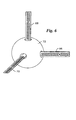
- Plural probes can be incorporated into a unit to provide a probe comprising three mutually orthogonal dipoles for E-field measurements in three axes.
- dipoles 66, 68 and 70 extend respectively along x, y and z axes from a spherical housing 72, which contains processing circuitry.
- Dipoles 66 and 68 can be formed on a single printed circuit board.
- FIG. 7 Another three-dimensional E-field probe, shown in FIG. 7, comprises three separate probes 74, 76 and 78, of the type shown in FIG. 5, disposed in mutually orthogonal relationship, crossing one another approximately at the dipole centers.
- the number of discrete resistors making up each dipole can vary, as can the number of discrete resistors making up the feeders. If the processing circuitry is small, the number of feeder resistors can be reduced, or the feeders can be eliminated altogether.
- the processing circuit is made small, it is possible to locate the processing circuit close to the dipole center rather than at an end of a dipole arm. Moreover, if a very small processing circuit is used, it can be provided on the circuit board at the location of the dipole center.
Landscapes
- Physics & Mathematics (AREA)
- Electromagnetism (AREA)
- General Physics & Mathematics (AREA)
- Variable-Direction Aerials And Aerial Arrays (AREA)
- Details Of Aerials (AREA)
- Measuring Leads Or Probes (AREA)
- Measuring Pulse, Heart Rate, Blood Pressure Or Blood Flow (AREA)
- Magnetic Resonance Imaging Apparatus (AREA)
- Ultra Sonic Daignosis Equipment (AREA)
Applications Claiming Priority (3)
| Application Number | Priority Date | Filing Date | Title |
|---|---|---|---|
| US09/968,816 US6593896B2 (en) | 2001-10-01 | 2001-10-01 | Field probe |
| US968816 | 2001-10-01 | ||
| PCT/US2002/031930 WO2003030299A1 (en) | 2001-10-01 | 2002-09-26 | Field probe |
Publications (3)
| Publication Number | Publication Date |
|---|---|
| EP1436855A1 EP1436855A1 (en) | 2004-07-14 |
| EP1436855A4 EP1436855A4 (en) | 2005-02-02 |
| EP1436855B1 true EP1436855B1 (en) | 2007-07-04 |
Family
ID=25514814
Family Applications (1)
| Application Number | Title | Priority Date | Filing Date |
|---|---|---|---|
| EP02773721A Expired - Lifetime EP1436855B1 (en) | 2001-10-01 | 2002-09-26 | Field probe |
Country Status (8)
| Country | Link |
|---|---|
| US (1) | US6593896B2 (enExample) |
| EP (1) | EP1436855B1 (enExample) |
| JP (1) | JP4068559B2 (enExample) |
| KR (1) | KR100650292B1 (enExample) |
| CN (1) | CN1561562A (enExample) |
| AT (1) | ATE366463T1 (enExample) |
| DE (1) | DE60221034D1 (enExample) |
| WO (1) | WO2003030299A1 (enExample) |
Families Citing this family (6)
| Publication number | Priority date | Publication date | Assignee | Title |
|---|---|---|---|---|
| NL2000793C2 (nl) | 2007-08-03 | 2009-02-09 | Dijkstra Advies | Probe voor het meten van een elektrisch veld. |
| US8305282B2 (en) * | 2010-07-23 | 2012-11-06 | Amplifier Research Corporation | Field probe |
| FR2967827B1 (fr) * | 2010-11-24 | 2013-08-02 | Univ Rennes | Antenne de communication a large bande passante. |
| US20130307763A1 (en) * | 2012-05-21 | 2013-11-21 | Amplifier Research Corporation | Field analyzer |
| CN106483387A (zh) * | 2016-11-16 | 2017-03-08 | 中国电子科技集团公司第四十研究所 | 一种电场辐射宽带检测器及其检测方法 |
| US11454661B2 (en) | 2020-11-05 | 2022-09-27 | Amplifier Research Corp. | Field probe |
Family Cites Families (12)
| Publication number | Priority date | Publication date | Assignee | Title |
|---|---|---|---|---|
| US3662260A (en) | 1971-02-12 | 1972-05-09 | Us Navy | Electric field measuring instrument with probe for sensing three orthogonal components |
| US3750017A (en) * | 1971-09-16 | 1973-07-31 | Us Health | Electromagnetic field measuring device |
| US3906509A (en) * | 1974-03-11 | 1975-09-16 | Raymond H Duhamel | Circularly polarized helix and spiral antennas |
| US4008477A (en) * | 1975-06-25 | 1977-02-15 | The United States Of America As Represented By The Secretary Of Commerce | Antenna with inherent filtering action |
| US4207518A (en) * | 1978-03-06 | 1980-06-10 | General Microwave Corporation | Broadband radiation detector with diode elements |
| US4466003A (en) * | 1982-02-09 | 1984-08-14 | The United States Of America As Represented By The Secretary Of The Navy | Compact wideband multiple conductor monopole antenna |
| US4634968A (en) * | 1982-12-20 | 1987-01-06 | The Narda Microwave Corporation | Wide range radiation monitor |
| US5644321A (en) | 1993-01-12 | 1997-07-01 | Benham; Glynda O. | Multi-element antenna with tapered resistive loading in each element |
| US6061025A (en) * | 1995-12-07 | 2000-05-09 | Atlantic Aerospace Electronics Corporation | Tunable microstrip patch antenna and control system therefor |
| US6084551A (en) | 1998-01-21 | 2000-07-04 | L-3 Communications, Inc. | Electromagnetic probe for the detection of e-field and h-field radiation |
| US6239749B1 (en) * | 1999-01-29 | 2001-05-29 | Ching-Kuang Tzuang | Fast-wave resonant antenna with stratified grounding planes |
| DE10114012B4 (de) * | 2000-05-11 | 2011-02-24 | Amtran Technology Co., Ltd., Chung Ho | Chipantenne |
-
2001
- 2001-10-01 US US09/968,816 patent/US6593896B2/en not_active Expired - Fee Related
-
2002
- 2002-09-26 CN CNA028193083A patent/CN1561562A/zh active Pending
- 2002-09-26 EP EP02773721A patent/EP1436855B1/en not_active Expired - Lifetime
- 2002-09-26 AT AT02773721T patent/ATE366463T1/de not_active IP Right Cessation
- 2002-09-26 KR KR1020047004821A patent/KR100650292B1/ko not_active Expired - Fee Related
- 2002-09-26 JP JP2003533377A patent/JP4068559B2/ja not_active Expired - Fee Related
- 2002-09-26 WO PCT/US2002/031930 patent/WO2003030299A1/en not_active Ceased
- 2002-09-26 DE DE60221034T patent/DE60221034D1/de not_active Expired - Lifetime
Non-Patent Citations (1)
| Title |
|---|
| None * |
Also Published As
| Publication number | Publication date |
|---|---|
| JP2005505962A (ja) | 2005-02-24 |
| DE60221034D1 (de) | 2007-08-16 |
| CN1561562A (zh) | 2005-01-05 |
| KR20040037231A (ko) | 2004-05-04 |
| US20030063039A1 (en) | 2003-04-03 |
| ATE366463T1 (de) | 2007-07-15 |
| EP1436855A1 (en) | 2004-07-14 |
| JP4068559B2 (ja) | 2008-03-26 |
| WO2003030299A1 (en) | 2003-04-10 |
| KR100650292B1 (ko) | 2006-11-27 |
| US6593896B2 (en) | 2003-07-15 |
| EP1436855A4 (en) | 2005-02-02 |
Similar Documents
| Publication | Publication Date | Title |
|---|---|---|
| US6807065B2 (en) | Multilayer printed circuit board | |
| US6980068B2 (en) | System for and method of interconnecting high-frequency transmission lines | |
| KR100855208B1 (ko) | 고성능 테스터 인터페이스 모듈 | |
| US20080079534A1 (en) | Lumped Resistance Electrical Cable | |
| US6437654B2 (en) | Substrate-type non-reciprocal circuit element and integrated circuit having multiple ground surface electrodes and co-planar electrical interface | |
| JP5466792B2 (ja) | ラジオ周波数用フィールドプローブ | |
| US6239587B1 (en) | Probe for monitoring radio frequency voltage and current | |
| NL2000793C2 (nl) | Probe voor het meten van een elektrisch veld. | |
| EP1436855B1 (en) | Field probe | |
| US6783371B2 (en) | Solder-down printed circuit board connection structure | |
| JPH0917535A (ja) | 半導体装置のソケット | |
| US6030254A (en) | Edge connector interposing probe | |
| US5488313A (en) | Test probe and circuit board arrangement for the circuit under test for microstrip circuitry | |
| EP0884854A2 (en) | Microwave detector | |
| JPH07335701A (ja) | プロービング装置 | |
| US6411113B1 (en) | Radio frequency test fixture | |
| KR100241362B1 (ko) | 평면형 자계프로브 | |
| KR20160091847A (ko) | 다이폴 안테나 | |
| JP6716107B2 (ja) | 測定用プローブ | |
| US5777470A (en) | Broadband probe for detecting the magnetic field component of an electromagnetic field | |
| JP2021019283A (ja) | アンテナ装置 | |
| JP2682588B2 (ja) | Icソケット | |
| SU1318940A1 (ru) | Датчик напр женности электрического пол высокой частоты | |
| JPH09510044A (ja) | データ処理装置内における信号伝送時間を低減するための接続方法および構造 | |
| JPH01298665A (ja) | 補助端子付きピン・グリット・アレイソケット |
Legal Events
| Date | Code | Title | Description |
|---|---|---|---|
| PUAI | Public reference made under article 153(3) epc to a published international application that has entered the european phase |
Free format text: ORIGINAL CODE: 0009012 |
|
| 17P | Request for examination filed |
Effective date: 20040326 |
|
| AK | Designated contracting states |
Kind code of ref document: A1 Designated state(s): AT BE BG CH CY CZ DE DK EE ES FI FR GB GR IE IT LI LU MC NL PT SE SK TR |
|
| AX | Request for extension of the european patent |
Extension state: AL LT LV MK RO SI |
|
| A4 | Supplementary search report drawn up and despatched |
Effective date: 20041216 |
|
| RIC1 | Information provided on ipc code assigned before grant |
Ipc: 7H 01Q 1/24 B Ipc: 7H 01Q 9/16 B Ipc: 7G 01R 29/08 B Ipc: 7H 01Q 1/38 A Ipc: 7H 01Q 23/00 B |
|
| REG | Reference to a national code |
Ref country code: HK Ref legal event code: DE Ref document number: 1065403 Country of ref document: HK |
|
| 17Q | First examination report despatched |
Effective date: 20050603 |
|
| GRAP | Despatch of communication of intention to grant a patent |
Free format text: ORIGINAL CODE: EPIDOSNIGR1 |
|
| GRAS | Grant fee paid |
Free format text: ORIGINAL CODE: EPIDOSNIGR3 |
|
| GRAA | (expected) grant |
Free format text: ORIGINAL CODE: 0009210 |
|
| AK | Designated contracting states |
Kind code of ref document: B1 Designated state(s): AT BE BG CH CY CZ DE DK EE ES FI FR GB GR IE IT LI LU MC NL PT SE SK TR |
|
| REG | Reference to a national code |
Ref country code: GB Ref legal event code: FG4D |
|
| REG | Reference to a national code |
Ref country code: CH Ref legal event code: EP |
|
| REG | Reference to a national code |
Ref country code: IE Ref legal event code: FG4D |
|
| REF | Corresponds to: |
Ref document number: 60221034 Country of ref document: DE Date of ref document: 20070816 Kind code of ref document: P |
|
| NLV1 | Nl: lapsed or annulled due to failure to fulfill the requirements of art. 29p and 29m of the patents act | ||
| REG | Reference to a national code |
Ref country code: CH Ref legal event code: PL |
|
| PG25 | Lapsed in a contracting state [announced via postgrant information from national office to epo] |
Ref country code: FI Free format text: LAPSE BECAUSE OF FAILURE TO SUBMIT A TRANSLATION OF THE DESCRIPTION OR TO PAY THE FEE WITHIN THE PRESCRIBED TIME-LIMIT Effective date: 20070704 Ref country code: PT Free format text: LAPSE BECAUSE OF FAILURE TO SUBMIT A TRANSLATION OF THE DESCRIPTION OR TO PAY THE FEE WITHIN THE PRESCRIBED TIME-LIMIT Effective date: 20071204 Ref country code: NL Free format text: LAPSE BECAUSE OF FAILURE TO SUBMIT A TRANSLATION OF THE DESCRIPTION OR TO PAY THE FEE WITHIN THE PRESCRIBED TIME-LIMIT Effective date: 20070704 Ref country code: BG Free format text: LAPSE BECAUSE OF FAILURE TO SUBMIT A TRANSLATION OF THE DESCRIPTION OR TO PAY THE FEE WITHIN THE PRESCRIBED TIME-LIMIT Effective date: 20071004 Ref country code: ES Free format text: LAPSE BECAUSE OF FAILURE TO SUBMIT A TRANSLATION OF THE DESCRIPTION OR TO PAY THE FEE WITHIN THE PRESCRIBED TIME-LIMIT Effective date: 20071015 |
|
| EN | Fr: translation not filed | ||
| PG25 | Lapsed in a contracting state [announced via postgrant information from national office to epo] |
Ref country code: AT Free format text: LAPSE BECAUSE OF FAILURE TO SUBMIT A TRANSLATION OF THE DESCRIPTION OR TO PAY THE FEE WITHIN THE PRESCRIBED TIME-LIMIT Effective date: 20070704 Ref country code: CH Free format text: LAPSE BECAUSE OF FAILURE TO SUBMIT A TRANSLATION OF THE DESCRIPTION OR TO PAY THE FEE WITHIN THE PRESCRIBED TIME-LIMIT Effective date: 20070704 Ref country code: LI Free format text: LAPSE BECAUSE OF FAILURE TO SUBMIT A TRANSLATION OF THE DESCRIPTION OR TO PAY THE FEE WITHIN THE PRESCRIBED TIME-LIMIT Effective date: 20070704 |
|
| PG25 | Lapsed in a contracting state [announced via postgrant information from national office to epo] |
Ref country code: BE Free format text: LAPSE BECAUSE OF FAILURE TO SUBMIT A TRANSLATION OF THE DESCRIPTION OR TO PAY THE FEE WITHIN THE PRESCRIBED TIME-LIMIT Effective date: 20070704 |
|
| PG25 | Lapsed in a contracting state [announced via postgrant information from national office to epo] |
Ref country code: DK Free format text: LAPSE BECAUSE OF FAILURE TO SUBMIT A TRANSLATION OF THE DESCRIPTION OR TO PAY THE FEE WITHIN THE PRESCRIBED TIME-LIMIT Effective date: 20070704 Ref country code: DE Free format text: LAPSE BECAUSE OF FAILURE TO SUBMIT A TRANSLATION OF THE DESCRIPTION OR TO PAY THE FEE WITHIN THE PRESCRIBED TIME-LIMIT Effective date: 20071008 Ref country code: GR Free format text: LAPSE BECAUSE OF FAILURE TO SUBMIT A TRANSLATION OF THE DESCRIPTION OR TO PAY THE FEE WITHIN THE PRESCRIBED TIME-LIMIT Effective date: 20071005 Ref country code: MC Free format text: LAPSE BECAUSE OF NON-PAYMENT OF DUE FEES Effective date: 20070930 |
|
| PLBE | No opposition filed within time limit |
Free format text: ORIGINAL CODE: 0009261 |
|
| STAA | Information on the status of an ep patent application or granted ep patent |
Free format text: STATUS: NO OPPOSITION FILED WITHIN TIME LIMIT |
|
| PG25 | Lapsed in a contracting state [announced via postgrant information from national office to epo] |
Ref country code: CZ Free format text: LAPSE BECAUSE OF FAILURE TO SUBMIT A TRANSLATION OF THE DESCRIPTION OR TO PAY THE FEE WITHIN THE PRESCRIBED TIME-LIMIT Effective date: 20070704 Ref country code: SK Free format text: LAPSE BECAUSE OF FAILURE TO SUBMIT A TRANSLATION OF THE DESCRIPTION OR TO PAY THE FEE WITHIN THE PRESCRIBED TIME-LIMIT Effective date: 20070704 |
|
| 26N | No opposition filed |
Effective date: 20080407 |
|
| GBPC | Gb: european patent ceased through non-payment of renewal fee |
Effective date: 20071004 |
|
| PG25 | Lapsed in a contracting state [announced via postgrant information from national office to epo] |
Ref country code: SE Free format text: LAPSE BECAUSE OF FAILURE TO SUBMIT A TRANSLATION OF THE DESCRIPTION OR TO PAY THE FEE WITHIN THE PRESCRIBED TIME-LIMIT Effective date: 20071004 |
|
| PG25 | Lapsed in a contracting state [announced via postgrant information from national office to epo] |
Ref country code: FR Free format text: LAPSE BECAUSE OF FAILURE TO SUBMIT A TRANSLATION OF THE DESCRIPTION OR TO PAY THE FEE WITHIN THE PRESCRIBED TIME-LIMIT Effective date: 20080229 |
|
| PG25 | Lapsed in a contracting state [announced via postgrant information from national office to epo] |
Ref country code: IE Free format text: LAPSE BECAUSE OF NON-PAYMENT OF DUE FEES Effective date: 20070926 |
|
| PG25 | Lapsed in a contracting state [announced via postgrant information from national office to epo] |
Ref country code: GB Free format text: LAPSE BECAUSE OF NON-PAYMENT OF DUE FEES Effective date: 20071004 |
|
| PG25 | Lapsed in a contracting state [announced via postgrant information from national office to epo] |
Ref country code: EE Free format text: LAPSE BECAUSE OF FAILURE TO SUBMIT A TRANSLATION OF THE DESCRIPTION OR TO PAY THE FEE WITHIN THE PRESCRIBED TIME-LIMIT Effective date: 20070704 |
|
| PG25 | Lapsed in a contracting state [announced via postgrant information from national office to epo] |
Ref country code: CY Free format text: LAPSE BECAUSE OF FAILURE TO SUBMIT A TRANSLATION OF THE DESCRIPTION OR TO PAY THE FEE WITHIN THE PRESCRIBED TIME-LIMIT Effective date: 20070704 |
|
| PG25 | Lapsed in a contracting state [announced via postgrant information from national office to epo] |
Ref country code: LU Free format text: LAPSE BECAUSE OF NON-PAYMENT OF DUE FEES Effective date: 20070926 |
|
| PG25 | Lapsed in a contracting state [announced via postgrant information from national office to epo] |
Ref country code: TR Free format text: LAPSE BECAUSE OF FAILURE TO SUBMIT A TRANSLATION OF THE DESCRIPTION OR TO PAY THE FEE WITHIN THE PRESCRIBED TIME-LIMIT Effective date: 20070704 |
|
| PG25 | Lapsed in a contracting state [announced via postgrant information from national office to epo] |
Ref country code: IT Free format text: LAPSE BECAUSE OF NON-PAYMENT OF DUE FEES Effective date: 20070930 |
|
| REG | Reference to a national code |
Ref country code: HK Ref legal event code: WD Ref document number: 1065403 Country of ref document: HK |