EP1432039B1 - Programmierbarer Speichertransistor - Google Patents
Programmierbarer Speichertransistor Download PDFInfo
- Publication number
- EP1432039B1 EP1432039B1 EP03078777A EP03078777A EP1432039B1 EP 1432039 B1 EP1432039 B1 EP 1432039B1 EP 03078777 A EP03078777 A EP 03078777A EP 03078777 A EP03078777 A EP 03078777A EP 1432039 B1 EP1432039 B1 EP 1432039B1
- Authority
- EP
- European Patent Office
- Prior art keywords
- lightly
- pmt
- substrate
- diffusion
- programmable memory
- Prior art date
- Legal status (The legal status is an assumption and is not a legal conclusion. Google has not performed a legal analysis and makes no representation as to the accuracy of the status listed.)
- Expired - Lifetime
Links
Images
Classifications
-
- H—ELECTRICITY
- H10—SEMICONDUCTOR DEVICES; ELECTRIC SOLID-STATE DEVICES NOT OTHERWISE PROVIDED FOR
- H10D—INORGANIC ELECTRIC SEMICONDUCTOR DEVICES
- H10D30/00—Field-effect transistors [FET]
- H10D30/60—Insulated-gate field-effect transistors [IGFET]
- H10D30/68—Floating-gate IGFETs
- H10D30/681—Floating-gate IGFETs having only two programming levels
- H10D30/683—Floating-gate IGFETs having only two programming levels programmed by tunnelling of carriers, e.g. Fowler-Nordheim tunnelling
-
- H—ELECTRICITY
- H10—SEMICONDUCTOR DEVICES; ELECTRIC SOLID-STATE DEVICES NOT OTHERWISE PROVIDED FOR
- H10B—ELECTRONIC MEMORY DEVICES
- H10B41/00—Electrically erasable-and-programmable ROM [EEPROM] devices comprising floating gates
- H10B41/30—Electrically erasable-and-programmable ROM [EEPROM] devices comprising floating gates characterised by the memory core region
-
- H—ELECTRICITY
- H10—SEMICONDUCTOR DEVICES; ELECTRIC SOLID-STATE DEVICES NOT OTHERWISE PROVIDED FOR
- H10B—ELECTRONIC MEMORY DEVICES
- H10B41/00—Electrically erasable-and-programmable ROM [EEPROM] devices comprising floating gates
- H10B41/60—Electrically erasable-and-programmable ROM [EEPROM] devices comprising floating gates the control gate being a doped region, e.g. single-poly memory cell
-
- H—ELECTRICITY
- H10—SEMICONDUCTOR DEVICES; ELECTRIC SOLID-STATE DEVICES NOT OTHERWISE PROVIDED FOR
- H10B—ELECTRONIC MEMORY DEVICES
- H10B69/00—Erasable-and-programmable ROM [EPROM] devices not provided for in groups H10B41/00 - H10B63/00, e.g. ultraviolet erasable-and-programmable ROM [UVEPROM] devices
-
- H—ELECTRICITY
- H10—SEMICONDUCTOR DEVICES; ELECTRIC SOLID-STATE DEVICES NOT OTHERWISE PROVIDED FOR
- H10D—INORGANIC ELECTRIC SEMICONDUCTOR DEVICES
- H10D30/00—Field-effect transistors [FET]
- H10D30/01—Manufacture or treatment
- H10D30/021—Manufacture or treatment of FETs having insulated gates [IGFET]
- H10D30/0411—Manufacture or treatment of FETs having insulated gates [IGFET] of FETs having floating gates
Definitions
- the present invention generally relates to semiconductor devices. More particularly, this invention relates to a programmable memory transistor having a floating gate that exhibits improved voltage retention.
- PMT Programmable memory transistors
- EPROM electrically programmable read only memory
- EEPROM electrically erasable programmable read only memory
- IGFET insulated gate field effect transistor
- nonvolatile refers to the retention of memory without the need of a power source, here by trapping a charge on a "floating" gate disposed above the IGFET channel region and typically below a conventional control gate electrode, such that the control and floating gates are “stacked.”
- the floating gate is described as “floating” because it is electrically insulated from the channel region by a gate oxide, typically insulated from the control gate by a “tunnel” oxide, and not directly accessed by any electrical conductor.
- PMT's can be electrically programmed after manufacture by placing an electrical charge on the floating gate by the effects of tunneling or avalanche injection from the control gate electrode through the tunnel oxide.
- the charge is trapped there until it is deliberately removed, such as by exposure to ultraviolet light.
- the trapped charge on the PMT floating gate raises the threshold voltage of the underlying channel region of the IGFET, thus raising the "turn on” voltage of the IGFET to a value above the voltage otherwise required for the IGFET. Accordingly, the IGFET stays “off” even when a normal turn-on voltage is applied to its control gate electrode.
- PMT's are typically fabricated in the same semiconductor substrate as MOS (metal-oxide-semiconductor) transistors, which are single-polysilicon layer structures and therefore require fewer patterning steps than PMT's. Therefore, PMT's have been proposed that make use of a single polysilicon layer, such as that disclosed in U.S. Patent No. 6,324,097 .
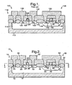
- An example of another single-polysilicon PMT is shown in Figure 1 , in which a PMT 110 is fabricated on a semiconductor substrate 112 doped with an N-type impurity.
- a P-well 114 is formed in a surface region of the substrate 112, and divided by a field oxide 116 into two active regions.
- An NMOS transistor 118 is formed in one of the active regions and conventionally includes source and drain regions 120 and 122 in the P-well 114, a channel 124 between the source and drain regions 120 and 122, and a gate electrode 126 separated from the channel 124 by a gate insulator 128 (e.g., silicon dioxide).
- Source and drain metal 130 and 132 make ohmic contact with the source and drain regions 120 and 122, respectively.
- the gate electrode 126 of the NMOS transistor 118 is a floating gate, in that it is not directly connected to a gate metal or other conductor.
- the gate electrode 126 is defined by a single polysilicon layer that also defines a second floating gate 146 of a control gate structure 138 fabricated in the second active region of the substrate 112 (on the right-hand side of Figure 1 ).
- the control gate structure 138 represented in Figure 1 includes two N+ contact diffusions 142 within an N-well 144 (though a single contact diffusion 142 or more than two contact diffusions 142 could be present).
- the N-well 144 serves as the control gate of the control gate structure 138, effectively replacing the second polysilicon layer of a conventional double-polysilicon PMT.
- the control gate (N-well) 144 is separated from the second floating gate 146 by a gate oxide 148, creating what is effectively a coupling capacitor.
- a control gate metal 150 contacts the N+ contact diffusions 142 to provide ohmic contact with the control gate 144.
- an electrical charge is placed on the floating gate 126 of the NMOS transistor 118 by the effect of tunneling or avalanche injection from the channel 124 of the gate electrode 126 through the gate insulator 128 to the floating gate 126.
- a sufficiently high potential must be applied to the control gate metal 150 to capacitively induce a charge in the floating gate 146 as well as the floating gate 126 as a result of the gates 126 and 146 being formed of the same polysilicon layer.
- the drain region 122 is biased at a high voltage level while the source region 120 and substrate 112 are electrically connected to ground, so that electrons are ejected from the drain region 122 through the gate insulator 128 into the floating gate 126.
- Vth the measured mean decay of a stored potential
- Vth the measured mean decay of a stored potential
- Vth degradation There are three distinct phases of Vth degradation for nominal PMT's, each associated with a different possible physical mechanism of charge distribution/conduction and each having its own empirical "activation energy.”
- the low field conduction mechanism is generally accepted as being conduction by thermionic emission.
- PMT's When subjected to elevated temperatures, e.g., 160°C or more, PMT's experience a significant initial drop in Vth attributed to the first degradation phase noted above. Thereafter, Vth stabilizes, though continuing to drop at a much lower rate attributed to the second and third degradation phases noted above. This lower rate is sufficiently low to permit the reliability of the device to be judged based on the initial Vth drop. Accordingly, PMT's typically undergo a data retention bake, or stress test, that involves baking at a sufficiently high temperature to cause the initial drop in Vth. A PMT is deemed to have passed the stress test if its Vth has not dropped below a predetermined level at the completion of the high temperature bake.
- a data retention bake or stress test
- US 5 719 427 discloses a single-polysilicon PMT including an NMOS transistor as well as a coupling capacitor.
- the coupling capacitor exhibits two highly-doped P+ content diffusions embedded in an N-well constituting a buried control gate.
- US 2002/005543 also discloses a single-polysilicon PMT including an NMOS transistor and a coupling capacitor.
- the coupling capacitor also exhibits two highly-doped P+ contact diffusions embedded in an N-well constituting a buried control gate.
- US 5 929 478 discloses a single-polysilicon PMT including an NMOS transistor (11) as well as a coupling capacitor (12).
- the coupling capacitor exhibits two oppositely-doped diffusion regions (46, 47) embedded in an N-well (28) constituting a buried control gate.
- the coupling area between the gate electrode (36) and the buried control gate (28) separated by a control gate insulator (35) is however not located between the two oppositely-doped diffusion regions (46, 47).
- the present invention is directed to a programmable memory transistor (PMT) that exhibits significantly better performance in terms of charge retention and reliability.
- the PMT of this invention is able to make use of a single polysilicon layer, and is capable of memory retention times of five orders of magnitude greater than similar single-polysilicon PMT's.
- the PMT also provides improved testability as a result of a greater measurement sensitivity for defects.
- the PMT of this invention generally comprises an insulated gate field effect transistor (IGFET) and a capacitor structure on a semiconductor substrate.
- IGFET insulated gate field effect transistor
- the IGFET comprises source and drain regions in a surface of the substrate, a channel between the source and drain regions, a gate insulator overlying the channel, and a first floating gate on the gate insulator.
- the capacitor structure comprises a lightly-doped well of a first conductivity type in the surface of the substrate, a heavily-doped first diffusion of the first conductivity type in the lightly-doped well, and a second diffusion of a second conductivity type in the lightly-doped well and spaced apart from the first diffusion so as to define therebetween a surface region of the lightly-doped well.
- the capacitor structure further comprises a control gate insulator that overlies the surface region of the lightly-doped well, a second floating gate on the control gate insulator, and a conductor in ohmic contact with the lightly-doped well through the first diffusion and in further contact with the lightly-doped well through the second diffusion.
- the first and second floating gates are electrically connected, preferably as a result of being formed of the same polysilicon layer, to maintain the first and second floating gates at the same potential.
- the second floating gate is capacitively coupled to the lightly-doped well through the control gate insulator so as to defme a control gate for the first floating gate.
- a sufficient voltage can be applied to the lightly-doped well to cause ejection of electrons from the drain region of the insulated gate field effect transistor and trap some of the ejected electrons in the first floating gate.
- PMT's fabricated with the oppositely-doped diffusions as described above do not experience the initial drop in Vth that occurs with conventional single-polysilicon PMT's when exposed to elevated temperatures, e.g., during a data retention bake.
- the PMT of this invention is capable of far superior data retention over comparable single-polysilicon PMT's.
- An additional benefit of the invention is the ability to simplify and/or shorten the aforementioned stress test performed on conventional PMT's to evaluate device reliability on the basis of the initial Vth drop.
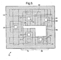
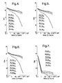
- FIGs 2 and 3 schematically represent a single-polysilicon PMT 10 capable of exhibiting superior memory retention in accordance with the present invention.
- the PMT 10 is similar to prior art double-polysilicon ("Poly1/Poly2") PMT's except that the second polysilicon layer is replaced with a lightly-doped well.
- the PMT 10 differs from prior art single-polysilicon PMT's (e.g., Figure 1 ) by the use of diffusions of opposite conductivity type within a lightly-doped well that defines the control gate for the PMT, the effect of which is improved memory retention resulting from the elimination of the initial Vth drop observed with prior art single-polysilicon PMT's.
- the PMT 10 is fabricated on a silicon (preferably monocrystalline) substrate 12 doped with an N-type impurity, e.g., phosphorus, arsenic or another pentavalent element.
- a suitable doping level for the substrate 12 is on the order of about 5x10 15 cm -2 .
- a P-well 14 is formed in a surface region of the substrate 12 by doping with boron or another trivalent element at a level of about 5x10 16 cm -2 .
- a field oxide 16 divides the P-well 14 into two active regions, one of which is occupied by an NMOS transistor 18, while the other is occupied by a coupling capacitor 38.
- the NMOS transistor 18 is formed to conventionally include source and drain regions 20 and 22 in the P-well 14, a channel 24 between the source and drain regions 20 and 22, and a polysilicon floating gate electrode 26 separated from the channel 24 by a gate oxide 28.
- the source and drain regions 20 and 22 are more heavily doped than the substrate 12, preferably at a level of about 1x10 20 cm -2 .
- Source and drain metal 30 and 32 make ohmic contact with the source and drain regions 20 and 22, respectively.
- a third region 23 heavily doped p-type for making ohmic contact with the P-well 14.
- the polysilicon floating gate electrode 26 of the NMOS transistor 18 is formed by a layer of polysilicon that also defines a floating gate electrode 46 of the coupling capacitor 38.
- the floating gate electrode 46 overlies a tunneling oxide 48 above a surface region of a lightly-doped N-type (NHV) diffusion 44.
- the NHV diffusion 44 is preferably doped at a level of about 2x10 17 cm -2 .
- Two diffusions 42 and 43 are shown as being formed within the NHV diffusion 44, a first of which is a contact diffusion 42 heavily doped n-type, such as on the order of about 1x10 20 cm -2 .
- the second diffusion is an injecting diffusion 43 heavily doped p-type, such as on the order of about 1x10 20 cm -2 .
- the floating gate electrode 46 serves as an upper capacitor plate of the coupling capacitor 38.
- the channel between the diffusions 42 and 43 in the NHV diffusion 44 serves as the second capacitor plate of the coupling capacitor 38 and the control gate for the NMOS transistor 18.
- a control gate metal 50 contacts both the N+ contact diffusion 42 and the P+ injecting diffusion 43 through a dielectric layer 52 overlying the surface of the substrate 12.
- the N + contact diffusion 42 provides ohmic contact with the NHV diffusion 44.
- the P+ injecting diffusion 43 does not provide ohmic contact with the NHV diffusion 44.
- the P+ injecting diffusion 43 provides what is termed herein a "stitch" contact, and is believed to source holes into a P-type inversion layer at the surface of the NHV diffusion 44 when the PMT 10 is being programmed.
- the presence of the P+ injecting diffusion 43 has been demonstrated to greatly improve the memory retention of the PMT 10 as compared to a PMT that differs by having a pair of N+ contact diffusions (e.g., Figure 1 ).
- all layers used in the PMT 10 are core process layers in NMOS processes, enabling the coupling capacitor 38 and the NMOS transistor 18 (as will as other MOS devices) to be fabricated simultaneously in the same substrate 12.
- PMT's in accordance with Figure 1 ("control") and Figure 2 were processed side-by-side on a PMT test array.
- the PMT's were fabricated on a monocrystalline silicon substrate with a twelve micrometer-thick N-type epitaxy having an impurity concentration of about 5x10 15 cm -2 .
- P-wells were formed in surface regions of the substrate by doping with boron at a level of about 5x10 16 cm -2 to a depth of about four micrometers.
- the source and drain regions of the NMOS transistors and the N + contact diffusions of the coupling capacitors were heavily doped with arsenic to a level of about 1x10 20 cm -2 and a depth of about 0.4 micrometers, while the P+ injecting diffusions of the PMT's of this invention and the P-well contact were heavily doped with boron to a level of about 1x10 20 cm -2 and a depth of about 0.4 micrometers.
- the floating gates were patterned from a single layer of polysilicon deposited by low pressure chemical vapor deposition (LPCVD) to a thickness of about 3500 Angstroms.
- LPCVD low pressure chemical vapor deposition
- All devices were erased with a deep UV bake and then programmed from an initial Vth of about 2V.
- Programming the PMT's involved applying drain and gate voltages to the NMOS for a few milliseconds or less. With the source region grounded, a positive voltage of less than the NMOS breakdown voltage (BVdss) was applied through a current limiting resistor to the drain region and a positive voltage on the order of about 3 MV/cm applied to the control gate metal of each device, with the result that "hot" electrons were ejected from the drain regions and became stored on the polysilicon floating gates.
- BVdss NMOS breakdown voltage
- the control PMT's reached a Vth of about 7.5V, while the PMT's processed in accordance with this invention reached a higher Vth of about 8.5V.
- the PMT's were then subjected to a standard data retention bake at temperatures of about 160°C, 180°C or 235°C.
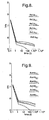
- the control PMT'S experienced a rapid initial drop in Vth of between about 1.5 and 2.0V after the first hour of baking. After the initial Vth drop, the control PMT's stabilized and Vth began to drop at a much slower rate.
- PMT's configured in accordance with this invention are capable of memory retention times of about five orders of magnitude greater than the control PMT's.
- An explanation was not evident as to why the PMT's of the invention did not experience an initial drop in Vth during the data retention bake.
- the P+ injecting diffusion sourced carriers to the lightly-doped NHV diffusion to create an inversion in the surface region of the NHV diffusion, which is suspected of resulting in a more complete electron injection, i.e., few (if any) electrons trapped inside the gate oxide.
- the higher Vth of the PMT's processed in accordance with the invention was attributed to the P+ stitch contact allowing a higher voltage on the control gate inversion channel.
- the PMT of this invention is characterized by improved testability as a result of a greater measurement sensitivity for defects. More particularly, the initial voltage drop exhibited by prior art PMT's necessitated a prolonged stress test to determine at what level their Vth's would stabilize. By eliminating the initial Vth drop, a defective PMT can be quickly identified by its displaying any rapid drop in Vth after programming.
Landscapes
- Non-Volatile Memory (AREA)
- Semiconductor Memories (AREA)
Claims (7)
- Programmierbarer Speicher-Transistor (10), der aufweist:ein Halbleitersubstrat (12);einen Feldeffekttransistor mit isoliertem Gate (insulated gate field effect transistor) (18) auf dem Substrat (12), wobei der der Feldeffekttransistor mit isoliertem Gate (18) aufweist einen Source-Bereich (20) in einer Oberfläche des Substrats (12), einen Drain-Bereich (22) in der Oberfläche des Substrats (12), einen Kanal (24) in der Oberfläche des Substrats (12) und zwischen den Source- und Drain-Bereichen (20, 22), einen Gate-Isolator (28), der den Kanal (24) überlagert, und ein erstes Floating Gate (26) auf dem Gate-Isolator (28);eine Kondensator-Struktur (38) auf dem Substrat (12), wobei die Kondensator-Struktur (38) aufweist eine schwach dotierte Wanne (44) eines ersten Leitfähigkeitstyps in der Oberfläche des Substrats (12), eine stark dotierte Kontaktdiffusion (42) des ersten Leitfähigkeitstyps in der schwach dotierten Wanne (44), eine injizierende Diffusion (43) eines zweiten Leitfähigkeitstyps in der schwach dotierten Wanne (44) und beabstandet von der Kontaktdiffusion (42), um dazwischen einen Oberflächenbereich der schwach dotierten Wanne (44) zu definieren, einen Steuerungs-Gate-Isolator (48), der über dem Oberflächenbereich der schwach dotierten Wanne (44) zwischen der Kontaktdiffusion (42) und der injizierenden Diffusion (43) liegt, ein zweites Floating Gate (46) auf dem Steuerungs-Gate-Isolator (48), und einen Leiter (50) in ohmschen Kontakt mit der schwach dotierten Wanne (44) über die Kontaktdiffusion (42) und in weiterem Kontakt mit der schwach dotierten Wanne (44) über die injizierende Diffusion (43); undMittel (26, 46) zum elektrischen Verbinden der ersten und zweiten Floating Gates (26, 46), um die ersten und zweiten Floating Gates (26, 46) auf demselben Potential zu halten;wobei das zweite Floating Gate (46) kapazitiv mit der schwach dotierten Wanne (44) über den Steuerungs-Gate-Isolator (48) verbunden ist, um so ein Steuerungs-Gate für das erste Floating Gate (26) zu definieren, wodurch ein Anlegen einer ausreichenden Spannung an die schwach dotierte Wanne (44) eine Abgabe von Elektronen aus dem Source-Bereich (20) des Feldeffekttransistors mit isoliertem Gate (18) und ein Einfangen von einigen der abgegebenen Elektronen in dem ersten Floating Gate (26) verursachen kann.
- Programmierbarer Speicher-Transistor (10) gemäß Anspruch 1, wobei die ersten und zweiten Floating Gates (26, 46) elektrisch verbunden sind als ein Resultat davon, dass sie durch eine Schicht von leitendem Material auf dem Substrat (12) definiert sind.
- Programmierbarer Speicher-Transistor (10) gemäß Anspruch 1, wobei das leitende Material Polysilizium ist.
- Programmierbarer Speicher-Transistor (10) gemäß Anspruch 1, der weiter Leiter (30, 32) in einem ohmschen Kontakt mit den Source- und Drain-Bereichen (20, 22) des Feldeffekttransistors mit isoliertem Gate (18) aufweist.
- Programmierbarer Speicher-Transistor (10) gemäß Anspruch 1, wobei der erste Leitfähigkeitstyp n-Typ ist und der zweite Leitfähigkeitstyp p-Typ ist.
- Programmierbarer Speicher-Transistor (10) gemäß Anspruch 1, wobei der Feldeffekttransistor mit isoliertem Gate (18) eine NMOS-Vorrichtung ist.
- Programmierbarer Speicher-Transistor (10) gemäß Anspruch 1, wobei der programmierbare Speicher-Transistor (10) eine einzelne Polysiliziumschicht aufweist.
Applications Claiming Priority (2)
| Application Number | Priority Date | Filing Date | Title |
|---|---|---|---|
| US324346 | 2002-12-19 | ||
| US10/324,346 US6762453B1 (en) | 2002-12-19 | 2002-12-19 | Programmable memory transistor |
Publications (3)
| Publication Number | Publication Date |
|---|---|
| EP1432039A2 EP1432039A2 (de) | 2004-06-23 |
| EP1432039A3 EP1432039A3 (de) | 2008-03-05 |
| EP1432039B1 true EP1432039B1 (de) | 2010-09-22 |
Family
ID=32393064
Family Applications (1)
| Application Number | Title | Priority Date | Filing Date |
|---|---|---|---|
| EP03078777A Expired - Lifetime EP1432039B1 (de) | 2002-12-19 | 2003-11-28 | Programmierbarer Speichertransistor |
Country Status (3)
| Country | Link |
|---|---|
| US (1) | US6762453B1 (de) |
| EP (1) | EP1432039B1 (de) |
| DE (1) | DE60334276D1 (de) |
Families Citing this family (17)
| Publication number | Priority date | Publication date | Assignee | Title |
|---|---|---|---|---|
| KR100553682B1 (ko) * | 2003-03-07 | 2006-02-24 | 삼성전자주식회사 | 게이트 전극을 갖는 반도체 소자 및 그 형성방법 |
| US20050145922A1 (en) * | 2003-12-30 | 2005-07-07 | Joseph Farley | EEPROM and flash EEPROM |
| KR100557532B1 (ko) * | 2004-04-20 | 2006-03-03 | 주식회사 하이닉스반도체 | 플래쉬 메모리 셀 트랜지스터 및 그 제조 방법 |
| US20070007577A1 (en) * | 2005-07-06 | 2007-01-11 | Matrix Semiconductor, Inc. | Integrated circuit embodying a non-volatile memory cell |
| JP2007149947A (ja) * | 2005-11-28 | 2007-06-14 | Nec Electronics Corp | 不揮発性メモリセル及びeeprom |
| JP2007149997A (ja) * | 2005-11-29 | 2007-06-14 | Nec Electronics Corp | 不揮発性メモリセル及びeeprom |
| US20070241392A1 (en) * | 2006-04-14 | 2007-10-18 | Hsin-Chang Lin | Non-volatile flash memory structure and method for operating the same |
| TW200805582A (en) * | 2006-07-04 | 2008-01-16 | Richtek Techohnology Corp | Non-volatile memory cell and its manufacturing process |
| US20080169500A1 (en) * | 2007-01-16 | 2008-07-17 | Atmel Corporation | Low voltage non-volatile memory cell with shared injector for floating gate |
| US8299519B2 (en) * | 2010-01-11 | 2012-10-30 | International Business Machines Corporation | Read transistor for single poly non-volatile memory using body contacted SOI device |
| EP2686882A4 (de) * | 2011-03-15 | 2014-11-12 | Hewlett Packard Development Co | Speicherzelle mit struktur einer geschlossenen kurve |
| US9230814B2 (en) | 2011-10-28 | 2016-01-05 | Invensas Corporation | Non-volatile memory devices having vertical drain to gate capacitive coupling |
| US8873302B2 (en) * | 2011-10-28 | 2014-10-28 | Invensas Corporation | Common doped region with separate gate control for a logic compatible non-volatile memory cell |
| US10468425B2 (en) * | 2014-02-04 | 2019-11-05 | Stmicroelectronics S.R.L. | Embedded non-volatile memory with single polysilicon layer memory cells erasable through band to band tunneling induced hot electron and programmable through Fowler-Nordheim tunneling |
| CN105632889A (zh) * | 2014-11-04 | 2016-06-01 | 北大方正集团有限公司 | 电容的制作方法、电容和电容组件 |
| DE102018124855B4 (de) * | 2017-11-16 | 2024-04-18 | Taiwan Semiconductor Manufacturing Co., Ltd. | Dual-Gate-Dielektrikum-Transistor und Verfahren |
| US20240321370A1 (en) * | 2023-03-22 | 2024-09-26 | Qualcomm Incorporated | Secure anti-fuse one time programmable bit cell design |
Family Cites Families (14)
| Publication number | Priority date | Publication date | Assignee | Title |
|---|---|---|---|---|
| EP0357333B1 (de) * | 1988-09-01 | 1994-12-28 | Atmel Corporation | Versiegelte Ladungsspeicheranordnung |
| US5719427A (en) * | 1997-01-14 | 1998-02-17 | Pericom Semiconductor Corp. | Avalanche-enhanced CMOS transistor for EPROM/EEPROM and ESD-protection structures |
| US5929478A (en) * | 1997-07-02 | 1999-07-27 | Motorola, Inc. | Single level gate nonvolatile memory device and method for accessing the same |
| US5796655A (en) * | 1997-10-20 | 1998-08-18 | Delco Electronics Corporation | Memory cell having programmed margin verification |
| US6044018A (en) | 1998-06-17 | 2000-03-28 | Mosel Vitelic, Inc. | Single-poly flash memory cell for embedded application and related methods |
| US6215700B1 (en) * | 1999-01-07 | 2001-04-10 | Vantis Corporation | PMOS avalanche programmed floating gate memory cell structure |
| US6326663B1 (en) * | 1999-03-26 | 2001-12-04 | Vantis Corporation | Avalanche injection EEPROM memory cell with P-type control gate |
| US6177703B1 (en) | 1999-05-28 | 2001-01-23 | Vlsi Technology, Inc. | Method and apparatus for producing a single polysilicon flash EEPROM having a select transistor and a floating gate transistor |
| US6034893A (en) * | 1999-06-15 | 2000-03-07 | Vantis Corporation | Non-volatile memory cell having dual avalanche injection elements |
| US6324097B1 (en) | 1999-08-26 | 2001-11-27 | Mosel Vitelic Inc. | Single poly non-volatile memory structure and its fabricating method |
| US6266225B1 (en) * | 1999-11-01 | 2001-07-24 | Delphi Technologies, Inc. | Method of programming relay based connectors |
| US6191980B1 (en) | 2000-03-07 | 2001-02-20 | Lucent Technologies, Inc. | Single-poly non-volatile memory cell having low-capacitance erase gate |
| US6570212B1 (en) * | 2000-05-24 | 2003-05-27 | Lattice Semiconductor Corporation | Complementary avalanche injection EEPROM cell |
| US6631087B2 (en) * | 2000-06-23 | 2003-10-07 | Gennum Corporation | Low voltage single poly deep sub-micron flash eeprom |
-
2002
- 2002-12-19 US US10/324,346 patent/US6762453B1/en not_active Expired - Lifetime
-
2003
- 2003-11-28 EP EP03078777A patent/EP1432039B1/de not_active Expired - Lifetime
- 2003-11-28 DE DE60334276T patent/DE60334276D1/de not_active Expired - Lifetime
Also Published As
| Publication number | Publication date |
|---|---|
| US6762453B1 (en) | 2004-07-13 |
| DE60334276D1 (de) | 2010-11-04 |
| US20040119113A1 (en) | 2004-06-24 |
| EP1432039A2 (de) | 2004-06-23 |
| EP1432039A3 (de) | 2008-03-05 |
Similar Documents
| Publication | Publication Date | Title |
|---|---|---|
| EP1432039B1 (de) | Programmierbarer Speichertransistor | |
| US4852062A (en) | EPROM device using asymmetrical transistor characteristics | |
| US6861315B1 (en) | Method of manufacturing an array of bi-directional nonvolatile memory cells | |
| US6438030B1 (en) | Non-volatile memory, method of manufacture, and method of programming | |
| US5019879A (en) | Electrically-flash-erasable and electrically-programmable memory storage devices with self aligned tunnel dielectric area | |
| US5173436A (en) | Method of manufacturing an EEPROM with trench-isolated bitlines | |
| US5284785A (en) | Diffusionless source/drain conductor electrically-erasable, electrically-programmable read-only memory and methods for making and using the same | |
| KR101538294B1 (ko) | 게이트 아래에서의 도펀트 확산을 감소시킴으로써 메모리 셀을 형성하는 방법 | |
| KR20050055003A (ko) | 비휘발성 메모리 디바이스 및 형성 방법 | |
| US5371031A (en) | Method of making EEPROM array with buried N+ windows and with separate erasing and programming regions | |
| US5411908A (en) | Flash EEPROM array with P-tank insulated from substrate by deep N-tank | |
| US5354703A (en) | EEPROM cell array with tight erase distribution | |
| US5045491A (en) | Method of making a nonvolatile memory array having cells with separate program and erase regions | |
| KR100350819B1 (ko) | 전계효과장치 | |
| US5017980A (en) | Electrically-erasable, electrically-programmable read-only memory cell | |
| US20130143375A1 (en) | On Current in One-Time-Programmable Memory Cells | |
| US5523249A (en) | Method of making an EEPROM cell with separate erasing and programming regions | |
| US20030155605A1 (en) | EEPROM memory cell with high radiation resistance | |
| US7713795B2 (en) | Flash memory device with single-poly structure and method for manufacturing the same | |
| US6025229A (en) | Method of fabricating split-gate source side injection flash memory array | |
| US5508955A (en) | Electronically erasable-programmable memory cell having buried bit line | |
| KR100243493B1 (ko) | 비대칭의 비휘발성 메모리셀, 어레이 및 그 제조방법 | |
| US5032533A (en) | Method of making a nonvolatile memory cell with field-plate switch | |
| US5147816A (en) | Method of making nonvolatile memory array having cells with two tunelling windows | |
| US5134449A (en) | Nonvolatile memory cell with field-plate switch |
Legal Events
| Date | Code | Title | Description |
|---|---|---|---|
| PUAI | Public reference made under article 153(3) epc to a published international application that has entered the european phase |
Free format text: ORIGINAL CODE: 0009012 |
|
| AK | Designated contracting states |
Kind code of ref document: A2 Designated state(s): AT BE BG CH CY CZ DE DK EE ES FI FR GB GR HU IE IT LI LU MC NL PT RO SE SI SK TR |
|
| AX | Request for extension of the european patent |
Extension state: AL LT LV MK |
|
| PUAL | Search report despatched |
Free format text: ORIGINAL CODE: 0009013 |
|
| AK | Designated contracting states |
Kind code of ref document: A3 Designated state(s): AT BE BG CH CY CZ DE DK EE ES FI FR GB GR HU IE IT LI LU MC NL PT RO SE SI SK TR |
|
| AX | Request for extension of the european patent |
Extension state: AL LT LV MK |
|
| RIC1 | Information provided on ipc code assigned before grant |
Ipc: H01L 21/336 20060101ALI20080129BHEP Ipc: H01L 21/8247 20060101ALI20080129BHEP Ipc: H01L 27/115 20060101AFI20040304BHEP Ipc: H01L 29/788 20060101ALI20080129BHEP |
|
| 17P | Request for examination filed |
Effective date: 20080905 |
|
| AKX | Designation fees paid |
Designated state(s): DE FR GB |
|
| 17Q | First examination report despatched |
Effective date: 20090114 |
|
| GRAP | Despatch of communication of intention to grant a patent |
Free format text: ORIGINAL CODE: EPIDOSNIGR1 |
|
| RIC1 | Information provided on ipc code assigned before grant |
Ipc: H01L 27/115 20060101ALI20100319BHEP Ipc: H01L 29/788 20060101AFI20100319BHEP |
|
| GRAS | Grant fee paid |
Free format text: ORIGINAL CODE: EPIDOSNIGR3 |
|
| GRAA | (expected) grant |
Free format text: ORIGINAL CODE: 0009210 |
|
| AK | Designated contracting states |
Kind code of ref document: B1 Designated state(s): DE FR GB |
|
| REG | Reference to a national code |
Ref country code: GB Ref legal event code: FG4D |
|
| REF | Corresponds to: |
Ref document number: 60334276 Country of ref document: DE Date of ref document: 20101104 Kind code of ref document: P |
|
| PGFP | Annual fee paid to national office [announced via postgrant information from national office to epo] |
Ref country code: DE Payment date: 20101124 Year of fee payment: 8 |
|
| PGFP | Annual fee paid to national office [announced via postgrant information from national office to epo] |
Ref country code: GB Payment date: 20101124 Year of fee payment: 8 |
|
| PLBE | No opposition filed within time limit |
Free format text: ORIGINAL CODE: 0009261 |
|
| STAA | Information on the status of an ep patent application or granted ep patent |
Free format text: STATUS: NO OPPOSITION FILED WITHIN TIME LIMIT |
|
| 26N | No opposition filed |
Effective date: 20110623 |
|
| REG | Reference to a national code |
Ref country code: DE Ref legal event code: R097 Ref document number: 60334276 Country of ref document: DE Effective date: 20110623 |
|
| PGFP | Annual fee paid to national office [announced via postgrant information from national office to epo] |
Ref country code: FR Payment date: 20111118 Year of fee payment: 9 |
|
| GBPC | Gb: european patent ceased through non-payment of renewal fee |
Effective date: 20121128 |
|
| REG | Reference to a national code |
Ref country code: FR Ref legal event code: ST Effective date: 20130731 |
|
| REG | Reference to a national code |
Ref country code: DE Ref legal event code: R119 Ref document number: 60334276 Country of ref document: DE Effective date: 20130601 |
|
| PG25 | Lapsed in a contracting state [announced via postgrant information from national office to epo] |
Ref country code: DE Free format text: LAPSE BECAUSE OF NON-PAYMENT OF DUE FEES Effective date: 20130601 |
|
| PG25 | Lapsed in a contracting state [announced via postgrant information from national office to epo] |
Ref country code: GB Free format text: LAPSE BECAUSE OF NON-PAYMENT OF DUE FEES Effective date: 20121128 Ref country code: FR Free format text: LAPSE BECAUSE OF NON-PAYMENT OF DUE FEES Effective date: 20121130 |