EP1427032A2 - Method of producing a piezoelectric part and piezoelectric part - Google Patents
Method of producing a piezoelectric part and piezoelectric part Download PDFInfo
- Publication number
- EP1427032A2 EP1427032A2 EP03293044A EP03293044A EP1427032A2 EP 1427032 A2 EP1427032 A2 EP 1427032A2 EP 03293044 A EP03293044 A EP 03293044A EP 03293044 A EP03293044 A EP 03293044A EP 1427032 A2 EP1427032 A2 EP 1427032A2
- Authority
- EP
- European Patent Office
- Prior art keywords
- piezoelectric
- acoustic wave
- mounting substrate
- surface acoustic
- resin film
- Prior art date
- Legal status (The legal status is an assumption and is not a legal conclusion. Google has not performed a legal analysis and makes no representation as to the accuracy of the status listed.)
- Granted
Links
Images






Classifications
-
- H—ELECTRICITY
- H03—ELECTRONIC CIRCUITRY
- H03H—IMPEDANCE NETWORKS, e.g. RESONANT CIRCUITS; RESONATORS
- H03H3/00—Apparatus or processes specially adapted for the manufacture of impedance networks, resonating circuits, resonators
- H03H3/007—Apparatus or processes specially adapted for the manufacture of impedance networks, resonating circuits, resonators for the manufacture of electromechanical resonators or networks
- H03H3/08—Apparatus or processes specially adapted for the manufacture of impedance networks, resonating circuits, resonators for the manufacture of electromechanical resonators or networks for the manufacture of resonators or networks using surface acoustic waves
-
- H—ELECTRICITY
- H03—ELECTRONIC CIRCUITRY
- H03H—IMPEDANCE NETWORKS, e.g. RESONANT CIRCUITS; RESONATORS
- H03H9/00—Networks comprising electromechanical or electro-acoustic elements; Electromechanical resonators
- H03H9/02—Details
- H03H9/05—Holders or supports
- H03H9/10—Mounting in enclosures
- H03H9/1064—Mounting in enclosures for surface acoustic wave [SAW] devices
- H03H9/1085—Mounting in enclosures for surface acoustic wave [SAW] devices the enclosure being defined by a non-uniform sealing mass covering the non-active sides of the SAW device
-
- H—ELECTRICITY
- H03—ELECTRONIC CIRCUITRY
- H03H—IMPEDANCE NETWORKS, e.g. RESONANT CIRCUITS; RESONATORS
- H03H9/00—Networks comprising electromechanical or electro-acoustic elements; Electromechanical resonators
- H03H9/02—Details
- H03H9/05—Holders or supports
- H03H9/058—Holders or supports for surface acoustic wave devices
- H03H9/059—Holders or supports for surface acoustic wave devices consisting of mounting pads or bumps
-
- H—ELECTRICITY
- H10—SEMICONDUCTOR DEVICES; ELECTRIC SOLID-STATE DEVICES NOT OTHERWISE PROVIDED FOR
- H10N—ELECTRIC SOLID-STATE DEVICES NOT OTHERWISE PROVIDED FOR
- H10N30/00—Piezoelectric or electrostrictive devices
- H10N30/01—Manufacture or treatment
- H10N30/07—Forming of piezoelectric or electrostrictive parts or bodies on an electrical element or another base
- H10N30/072—Forming of piezoelectric or electrostrictive parts or bodies on an electrical element or another base by laminating or bonding of piezoelectric or electrostrictive bodies
- H10N30/073—Forming of piezoelectric or electrostrictive parts or bodies on an electrical element or another base by laminating or bonding of piezoelectric or electrostrictive bodies by fusion of metals or by adhesives
-
- H—ELECTRICITY
- H10—SEMICONDUCTOR DEVICES; ELECTRIC SOLID-STATE DEVICES NOT OTHERWISE PROVIDED FOR
- H10W—GENERIC PACKAGES, INTERCONNECTIONS, CONNECTORS OR OTHER CONSTRUCTIONAL DETAILS OF DEVICES COVERED BY CLASS H10
- H10W72/00—Interconnections or connectors in packages
- H10W72/01—Manufacture or treatment
- H10W72/0198—Manufacture or treatment batch processes
-
- H—ELECTRICITY
- H10—SEMICONDUCTOR DEVICES; ELECTRIC SOLID-STATE DEVICES NOT OTHERWISE PROVIDED FOR
- H10W—GENERIC PACKAGES, INTERCONNECTIONS, CONNECTORS OR OTHER CONSTRUCTIONAL DETAILS OF DEVICES COVERED BY CLASS H10
- H10W72/00—Interconnections or connectors in packages
- H10W72/071—Connecting or disconnecting
- H10W72/072—Connecting or disconnecting of bump connectors
- H10W72/07251—Connecting or disconnecting of bump connectors characterised by changes in properties of the bump connectors during connecting
-
- H—ELECTRICITY
- H10—SEMICONDUCTOR DEVICES; ELECTRIC SOLID-STATE DEVICES NOT OTHERWISE PROVIDED FOR
- H10W—GENERIC PACKAGES, INTERCONNECTIONS, CONNECTORS OR OTHER CONSTRUCTIONAL DETAILS OF DEVICES COVERED BY CLASS H10
- H10W72/00—Interconnections or connectors in packages
- H10W72/20—Bump connectors, e.g. solder bumps or copper pillars; Dummy bumps; Thermal bumps
-
- H—ELECTRICITY
- H10—SEMICONDUCTOR DEVICES; ELECTRIC SOLID-STATE DEVICES NOT OTHERWISE PROVIDED FOR
- H10W—GENERIC PACKAGES, INTERCONNECTIONS, CONNECTORS OR OTHER CONSTRUCTIONAL DETAILS OF DEVICES COVERED BY CLASS H10
- H10W74/00—Encapsulations, e.g. protective coatings
-
- H—ELECTRICITY
- H10—SEMICONDUCTOR DEVICES; ELECTRIC SOLID-STATE DEVICES NOT OTHERWISE PROVIDED FOR
- H10W—GENERIC PACKAGES, INTERCONNECTIONS, CONNECTORS OR OTHER CONSTRUCTIONAL DETAILS OF DEVICES COVERED BY CLASS H10
- H10W90/00—Package configurations
- H10W90/701—Package configurations characterised by the relative positions of pads or connectors relative to package parts
- H10W90/721—Package configurations characterised by the relative positions of pads or connectors relative to package parts of bump connectors
- H10W90/724—Package configurations characterised by the relative positions of pads or connectors relative to package parts of bump connectors between a chip and a stacked insulating package substrate, interposer or RDL
-
- Y—GENERAL TAGGING OF NEW TECHNOLOGICAL DEVELOPMENTS; GENERAL TAGGING OF CROSS-SECTIONAL TECHNOLOGIES SPANNING OVER SEVERAL SECTIONS OF THE IPC; TECHNICAL SUBJECTS COVERED BY FORMER USPC CROSS-REFERENCE ART COLLECTIONS [XRACs] AND DIGESTS
- Y10—TECHNICAL SUBJECTS COVERED BY FORMER USPC
- Y10T—TECHNICAL SUBJECTS COVERED BY FORMER US CLASSIFICATION
- Y10T156/00—Adhesive bonding and miscellaneous chemical manufacture
- Y10T156/10—Methods of surface bonding and/or assembly therefor
- Y10T156/1052—Methods of surface bonding and/or assembly therefor with cutting, punching, tearing or severing
-
- Y—GENERAL TAGGING OF NEW TECHNOLOGICAL DEVELOPMENTS; GENERAL TAGGING OF CROSS-SECTIONAL TECHNOLOGIES SPANNING OVER SEVERAL SECTIONS OF THE IPC; TECHNICAL SUBJECTS COVERED BY FORMER USPC CROSS-REFERENCE ART COLLECTIONS [XRACs] AND DIGESTS
- Y10—TECHNICAL SUBJECTS COVERED BY FORMER USPC
- Y10T—TECHNICAL SUBJECTS COVERED BY FORMER US CLASSIFICATION
- Y10T156/00—Adhesive bonding and miscellaneous chemical manufacture
- Y10T156/10—Methods of surface bonding and/or assembly therefor
- Y10T156/1089—Methods of surface bonding and/or assembly therefor of discrete laminae to single face of additional lamina
- Y10T156/1092—All laminae planar and face to face
- Y10T156/1093—All laminae planar and face to face with covering of discrete laminae with additional lamina
Definitions
- the present invention relates to a piezoelectric part suitable for use in a filter of an electronic device, e.g., a mobile communications device such as a portable telephone or the like and to a method of producing the same.
- Surface acoustic wave devices utilize surface acoustic waves which are propagated along the piezoelectric substrates. Thus, it is necessary to protect the surface portions (functioning portions) of the devices on which surface acoustic waves are propagated from water, dust, and so forth.
- a surface acoustic wave element piezoelectric element
- a cover (lid) made of a metal or ceramics material is soldered to the package, and the package is air-tightly sealed by welding, soldering, or the like, or by use of glass or the like.
- a method is disclosed (e.g., see Japanese Unexamined Patent Application Publication No. 8-204497 (Publication Date: August 9, 1996 (Patent Documents 1), and Japanese Unexamined Patent Application Publication No. 7-321583 (Publication Date: December 8, 1995) (Patent Documents 2)), in which plural surface acoustic wave elements, which are mounted on a mounting substrate by flip chip bonding, are sealed with a resin, and thereafter, the elements are diced into the respective chips.
- This method is disadvantageous in that a liquid resin invades the surface acoustic wave propagation portion (functioning portion), and thereby, a rejected device is produced.
- a countermeasure against the formation of such a rejected device has been disclosed, in which a dam is provided on a surface acoustic wave element or a mounting substrate (e.g., see Japanese Unexamined Patent Application Publication No. 10-321666 (Publication Date: December 4, 1998 (Patent Documents 3)).
- Patent Documents 3 Japanese Unexamined Patent Application Publication No. 10-321666 (Publication Date: December 4, 1998 (Patent Documents 3)).
- this countermeasure will be ineffective in solving the above-described problem.
- a rejected device is formed, which is caused by the liquid resin invading the surface acoustic wave propagation area (vibrating portion, functioning portion) of the surface acoustic wave element.
- the known method of forming a dam has problems in that the heights of the dams and the bonding bumps may be different from each other, causing the adhesion strengths of the bumps to be reduced, and moreover, the formation of the dam increases the size of the surface acoustic wave element.
- a method in which a resin film is bonded to a surface acoustic wave element mounted by flip chip bonding, so that the mounted element is sealed, and thereafter, the elements are diced into the respective chips (e.g., see Japanese Unexamined Patent Application Publication No. 8-204497 (Publication Date: May 15, 1998 (Patent Documents 4), International Patent Application Publication WO97/02596 (Publication Date: January 23, 1997 (Patent Documents 5), Japanese Unexamined Patent Application Publication No. 2002-217221 (Publication Date: August 2, 2002 (Patent Documents 6), Japanese Unexamined Patent Application Publication No.
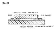
- Patent Document 4 a resin film is bonded to a mounting substrate by use of an adhesive or the like, as shown in Fig. 28.
- Patent Document 5 a resin film is heated to be deformed, so that the film is bonded to a mounting substrate.
- a hot-melted resin film is made to cover from the upper side, air-bubbles may be trapped by the resin film.
- the resin film may become substantially liquid, unless the melting of the resin film is properly controlled. Thus, the resin is in danger of flowing into a vibration space.
- Patent Documents 6 and 7 a resin film is heated and moreover pressed by means of a jig, so that the resin film is bonded to a mounting substrate.
- the substrate and the film it is necessary for the substrate and the film to have a large area in which they are heated and pressed for bonding the mounting substrate and the resin film to each other. Accordingly, it is difficult to produce a small-sized surface acoustic wave device.
- the surface acoustic wave devices produced by the above-described methods are sealed with the thin resin films, respectively. Thus, the air-tightness is insufficient.
- Patent Document 8 the surface acoustic wave device sealed with a resin film is further sealed with a resin.
- this method is disadvantageous in reduction of the height of the device, since the height is increased by the thickness of the resin, in addition to that of the resin film.
- Patent Document 9 a resin film is vacuum-formed. Further, according to Patent Document 10, a resin film is preformed so that no air-bubbles are formed.
- Patent Document 10 these methods have problems in that an exclusive-use apparatus is required for the processing, the number of processes is increased, and the manufacturing cost is high.
- the above-described problems also occur in piezoelectric parts such as piezoelectric resonators and piezoelectric filters in each of which piezoelectric resonators are arranged in a ladder-form.
- the piezoelectric resonator contains an Si substrate having an opening or concavity, and a vibration portion.
- the vibration portion is positioned so as to cover the opening or concavity, and has a structure in which a pair of upper and lower electrodes, set to be in opposition to each other, are placed on the upper and lower surfaces of a piezoelectric thin-film having at least one layer (e.g., made of ZnO and AIN) so that the thin film is sandwiched between the upper and lower electrodes.
- the present invention has been devised. It is an object of the present invention to provide a method of producing a piezoelectric part in which a mounting substrate and a surface acoustic wave element (piezoelectric element) are securely sealed with a resin film, and of which the reliability is high and the production cost is low, and to provide a piezoelectric part.
- a method of producing a piezoelectric part which includes the steps of: forming a piezoelectric element comprising a vibrating portion and a bump on a substrate; mounting plural piezoelectric elements on a mounting substrate having external terminals via the bumps by flip chip bonding in such a manner that the vibrating portions are opposed to the mounting substrate; arranging a resin film on the mounting substrate having the piezoelectric elements mounted thereon; sealing the piezoelectric elements by embedding the resin film between neighboring piezoelectric elements mounted on the mounting substrate; hardening the resin film; and splitting the mounting substrate by dicing to take out the individual piezoelectric parts, the sealing step involving a step of hot-press bonding in which the resin film is heated and softened, and simultaneously is pressed by means of a roller.
- the piezoelectric elements are mounted by flip chip bonding onto the mounting substrate having the external terminals.
- the resin sealing the piezoelectric elements the resin film is used. The resin film is heated and pressed to be deformed, so that the piezoelectric elements are embedded (the resin film is filled between piezoelectric elements) to be sealed.
- a liquid resin is not used, but the resin film is used to seal the piezoelectric elements. Therefore, the resin is prevented from flowing into the vibrating portion of a piezoelectric element. Thereby, it is unnecessary to provide a dam or the like, and the size of the piezoelectric part can be reduced. Moreover, since no liquid resin is used, generation of voids (holes or the like) can be inhibited.
- the heating and the pressing are simultaneously carried out by means of a roller. Accordingly, this step can be easily carried out compared to a process of bonding a resin film to a mounting substrate. The whole of the piezoelectric element can be securely covered with the resin. Thus, the piezoelectric element can be sufficiently protected. Accordingly, the piezoelectric part of which the reliability is high, the size is small, and the production cost is low can be provided.
- the mounting substrate having the piezoelectric elements mounted thereon is passed through between two rollers.
- the mounting substrate having the piezoelectric elements mounted thereon is fixed on a flat-surface stage for the hot-press bonding.
- the mounting substrate may be passed through between two rollers to be heated and pressed, or a roller may be applied onto the mounting substrate, while the substrate is placed on a flat surface, so that the resin film can be hot-press bonded to the mounting substrate.
- the resin film is heated and pressed by means of a roller, and thus, the piezoelectric part can be easily produced.
- the roller is applied to the mounting substrate from one end thereof. Accordingly, the air existing between the mounting substrate and the resin film can be efficiently escaped therefrom. Thus, generation of voids in the sealing resin formed of the resin film can be prevented.
- a step of pressing the resin film from the upper side thereof is carried out by use of a mold-frame after the hot-press bonding step.
- the hot-press bonding step is carried out by use of a mold-frame after a hot-press bonding step.
- the pressing (press) process is carried out using the mold-frame, the adhesion of the resin film to the mounting substrate can be more enhanced.
- a hot-press bonding step is carried out again after the above-described hot-press bonding step.
- the hot-press bonding step and the pressing step are sequentially carried out, using the mold-frame.
- a hot-press bonding step is carried out again after the hot-press bonding, and thereafter, the step of pressing the resin film from the upper side thereof is carried out by use of the mold-frame.
- the mounting substrate will be broken if the embedding pressure is excessively high, or the embedding of the resin film will be insufficient, if the pressure is small.
- the resin film is embedded by plural embedding-processes.
- the above-described inconveniences can be eliminated.
- the method of producing a piezoelectric part further includes, after the arranging step, a step of disposing a resin-flowing-out preventing frame on the end portion of the mounting substrate.
- the resin flowing-out preventing frame effectively prevents the resin from flow out when the resin film is heated and pressed by means of a roller. Moreover, the resin has a constant thickness. Especially, when an outer frame having the surface coated with a fluororesin such as polytetrafluoroethylene or the like is employed, the resin softened and stuck to the outer frame in a subsequent process can be easily peeled off therefrom.
- a sealing-assisting piece is formed between neighboring piezoelectric elements mounted on the mounting substrate.
- the sealing-assisting piece may be formed before or after the mounting step.
- the sealing-assisting pieces may be provided by bonding a sheet having plural openings to the mounting substrate.
- piezoelectric elements may be mounted to the mounting substrate through the openings, respectively.
- the height of the sealing-assisting pieces is larger than that of the bumps and is smaller than that of the piezoelectric elements mounted by flip chip bonding.
- the distance between the resin film and the sealing-assisting piece is small.
- the gaps between the resin film and the sealing-assisting pieces are hardly formed.
- the adhesion is enhanced, so that the fixing strength between the resin film and the sealing-assisting pieces can be increased. That is, the fixing strength between the resin film and the mounting substrate is enhanced.
- the mounting substrate is surface-modification-treated by plasma-irradiation, UV-irradiation, corona-discharge, excimer-laser irradiation, or sand-blasting before or after the mounting step.
- the surface-modification-treatment of the mounting substrate enhances the adhesion between the resin film and the mounting substrate.
- the gaps between the piezoelectric elements mounted on the mounting substrate via the bumps by flip chip bonding and the mounting substrate are in the range of 10 ⁇ m to 50 ⁇ m.
- the resin can be prevented from flowing in between the mounting substrate and the piezoelectric elements.
- the distance D between plural piezoelectric elements mounted on the mounting substrate and the thickness t of the piezoelectric elements involving the bumps have a relationship expressed by D/t > 2.
- the resin can be filled-in between piezoelectric elements without formation of voids.
- the height d of the piezoelectric part, the volume V of a piezoelectric element including the bumps and the gap between the piezoelectric element and the mounting substrate, the number, n, of piezoelectric elements per unit area on the mounding substrate, the thickness t1 of the resin film, and the average thickness t2 of the mounting substrate (cross-sectional area/length of substrate) have a relationship expressed by 0.8 ⁇ d/(nV + t1 + t2) ⁇ 1.1.
- the piezoelectric elements can be sealed with the resin, while the resin film is prevented from being broken or being partially wound.
- the resin film has a volume-resistivity of up to 10 10 ⁇ m.
- the method of the present invention may further comprise a step of forming an electroconductive layer on the back surface of a piezoelectric element after the mounting step.
- the method of producing a piezoelectric part according to the present invention may further comprise a step of forming an electroconductive layer on the hardened resin film after the hardening step.
- the piezoelectric element may be a surface acoustic wave element having at least one interdigital electrode on the surface of a piezoelectric substrate.
- the piezoelectric element may be a piezoelectric thin-film element comprising a substrate having an opening or concavity, and a vibrating portion having a structure in which a piezoelectric thin-film having at least one layer is sandwiched between a pair of upper and lower electrodes opposed to each other, the vibrating portion being positioned over the opening or concavity.
- a piezoelectric part which is produced according to any one of the above-described production methods.
- a piezoelectric part of which the reliability is high, the size is small, and the production cost is low can be provided.
- another piezoelectric part which includes a piezoelectric element having a vibrating portion formed on the surface of a substrate; a mounting substrate having an external terminal, and onto which the piezoelectric element is mounted by flip chip bonding via a bump while the surface of the piezoelectric element on which the vibrating portion is formed is opposed to the mounting substrate; and a resin sealing the piezoelectric element mounted onto the mounting substrate, the resin having a volume resistivity of up to 10 10 ⁇ m.
- the resin has a volume resistivity of up to 10 10 ⁇ m.
- electric charges generated on the piezoelectric elements can quickly migrate to the resin film, so that the electric charges are neutralized (escape).
- the generated electric charges can be prevented from causing discharge.
- a piezoelectric part can be provided, of which the piezoelectric element is prevented from being broken by discharge.
- a piezoelectric part which includes a piezoelectric element having a vibrating portion formed on the surface of a substrate; a mounting substrate having an external terminal and onto which the piezoelectric element is mounted by flip chip bonding via a bump while the surface of the piezoelectric element on which the vibrating portion is formed is opposed to the mounting substrate; and a resin sealing the piezoelectric element mounted onto the mounting substrate, the piezoelectric element having a back-surface conductive layer formed on the back surface thereof.
- a piezoelectric part can be provided, of which the piezoelectric element is prevented from being broken by discharge.
- a piezoelectric part which includes a piezoelectric element having a vibrating portion formed on the surface of a substrate; a mounting substrate having an external terminal and onto which the piezoelectric element is mounted by flip chip bonding via a bump while the surface of the piezoelectric element on which the vibrating portion is formed is opposed to the mounting substrate; and a resin sealing the piezoelectric element mounted onto the mounting substrate, the resin having a surface conductive layer formed thereon.
- a piezoelectric part can be provided, of which the piezoelectric element is prevented from being broken by discharge.
- At least one of the back-surface conductive layer and the surface conductive layer has an area-resistivity of up to 10 10 ⁇ /square.
- the resin has a volume-resistivity of up to 10 10 ⁇ m.
- the back-surface conductive layer or the surface conductive layer is connected to a ground terminal as an external terminal of the mounting substrate.
- the generated electric charges can be more effectively prevented from causing discharge.
- a piezoelectric part can be provided, of which the piezoelectric element is prevented from being broken by discharge.
- a method of producing a surface acoustic wave device which includes the steps of: forming a surface acoustic wave element containing at least one interdigital electrode and a bump formed on the surface of a piezoelectric substrate; mounting plural surface acoustic wave elements on a mounting substrate having external terminals via the bumps by flip chip bonding in such a manner that the interdigital electrodes are opposed to the mounting substrate; arranging a resin film on the mounting substrate having the surface acoustic wave elements mounted thereon; sealing the surface acoustic wave elements by embedding the resin film between neighboring surface acoustic wave elements mounted on the mounting substrate; hardening the resin film; and splitting the mounting substrate by dicing to take out the individual surface acoustic wave devices.
- the sealing step is a hot-press bonding step in which the resin film is heated to be softened, and simultaneously pressed by use of a jig.
- the surface acoustic wave elements are mounted onto a mounting substrate having external terminals by flip chip bonding.
- the resin sealing the surface acoustic wave elements the resin film is used.
- the resin film is heated and pressed to be deformed by use of a jig, so that the surface acoustic wave elements are embedded (the resin film is filled between surface acoustic wave elements) to be sealed.
- a liquid resin is not used, but the resin film is used to seal the surface acoustic wave elements. Therefore, the resin is prohibited from flowing into the vibrating portion of a piezoelectric element. Thereby, it is unnecessary to provide a dam or the like, and the size of the surface acoustic wave device can be reduced. Moreover, since no liquid resin is used, generation of voids (holes or the like) can be inhibited.
- the heating and the pressing are simultaneously carried out by means of a jig. Accordingly, this step can be easily carried out compared to a process of bonding a resin film to a mounting substrate.
- the whole of the surface acoustic wave element can be securely covered with the resin.
- the surface acoustic wave element can be sufficiently protected. Accordingly, the surface acoustic wave device has a high reliability, is reduced in size, and is produced at a low production cost.
- the method of producing a piezoelectric part, a piezoelectric part, and the method of producing a surface acoustic wave device are suitably used in the communications fields, i.e., for filters in communications devices such as portable telephones or the like.
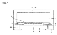
- Fig. 1 is a cross-sectional view of a surface acoustic wave device designed as a piezoelectric part according to this embodiment.
- the surface acoustic wave device of this embodiment comprises a mounting substrate 1 and a surface acoustic wave element (piezoelectric element) 2 mounted on the mounting substrate 1 by flip chip bonding.
- a mounting substrate 1 is made of a ceramics material, a resin, or the like such as alumina, glass-epoxy, and so forth.
- the surface acoustic wave element 2 comprises at least one interdigital electrode and plural bumps formed on a piezoelectric substrate. The surface of the surface acoustic wave element 2 on which the interdigital electrode is formed is used as a mounting surface.
- the mounting substrate 1 and the surface acoustic wave element 2 are connected by bonding bumps 3 formed on the surface acoustic wave element 2 and lands 4 formed on the mounting substrate 1 opposed to each other.
- the mounting substrate 1 is provided with external electrodes 7 which are electrically connected to the lands 4 via viaholes 30.
- the interdigital electrode is formed on the surface of the surface acoustic wave element 2 which is in opposition to the mounting substrate 1.
- the region of the surface acoustic wave element 2, in which the interdigital electrode is formed, and a surface acoustic wave is propagated, is named as a functioning portion (vibrating portion) 6.
- the bumps 3 are made of solder, gold, an electroconductive resin, or the like.
- the bumps 3 may have a function of electrically connecting the surface acoustic wave element 2 to the mounting substrate 1, a function of mechanically fixing the surface acoustic wave element 2 to the mounting substrate 1, and/or a function of maintaining the mounting substrate 1 and the surface acoustic wave element 2 in separation from each other at an interval between them.
- the surface acoustic wave element 2 is covered and sealed with a sealing resin 5 (resin film 10).
- a gap (space) 8 is formed between the above-described functioning portion 6 and the mounting substrate 1, which allows a surface acoustic wave to be propagated.
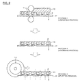
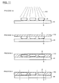
- the method of producing a surface acoustic wave device contains processes 1 to 3 as illustrated in Fig. 2.
- the process 1 first, plural surface acoustic wave elements 2 are mounted on an assembly substrate 41 (mounting process). After the mounting process, the assembly substrate 41 is cut to be separated in the surface direction, so that the mounting substrates 1 are formed.
- the bumps 3 formed on each surface acoustic wave element 2 are bonded to lands not shown) formed on the assembly substrate 41.
- the surface acoustic wave elements 2 are mounted on the assembly substrate 41 by flip chip bonding. In this case, gaps (space) of at least 10 ⁇ m are formed between the assembly substrate 41 and the surface acoustic wave elements 2, due to the bumps 3.
- the surface acoustic wave element 2 and the assembly substrate 41 have a high possibility of coming into contact with each other, due to the warp, the surface-irregularities, and so forth of the assembly substrate 41.
- the characteristics of a produced surface acoustic wave device will be insufficient, to be evaluated as a rejected product.
- bonding the bumps 3 and the lands to each other for example, Au-Au bonding, soldering, plating bump bonding, hot press bonding, supersonic welding, and so forth may be selected for use.
- at least one interdigital electrode and plural bumps may be formed on a piezoelectric substrate.
- a resin film (resin sheet) 10 is arranged on the surface acoustic wave elements 2 mounted on the assembly substrate 41 (arranging process). That is, the resin film 10 is placed so as to cover the surface acoustic wave elements 2.
- the resin film 10 may be made from a material having a heat-softening property and an adhesive property such as an epoxy resin composition, a polyimide type resin composition, a polyolefin type resin composition, and so forth. Most preferably, the film is made from an epoxy resin composition.
- the modulus of elasticity of the resin film 10 is in the range of 0.05 MPa to 2 MPa. If the resin film 10 is excessively flexible, problematically, the film has a greater possibility of adhering to the functioning portion. On the other hand, if the resin film 10 is excessively rigid, a problem will occur in that the resin can not be embedded between the surface acoustic wave elements 2.
- the assembly substrate 41 having the resin film 10 placed thereon is passed through between the two rollers (jigs) 11 set at a predetermined temperature and also a predetermined spacing in advance, so that the resin film 10 is hot-press-bonded to the assembly substrate 41 for sealing (sealing process).
- the resin film 10 While the resin film 10 is passed through as described above, the resin film 10 is heated with the rollers 11 so as to be softened, and moreover, the resin film 10 is embedded in the peripheries of the surface acoustic wave elements 2, that is, it extends down between the surface acoustic wave elements 2, so that the resin film 10 is hot-press bonded to the assembly substrate 41.
- the surface acoustic wave elements 2 are sealed on the inside of the sealing resin 5 of the resin film 10.
- the resin film may be supplied in a sheet form or in a continuous film form (roll-supply). A series of the processes described above is named a laminating process.
- the resin film 10 is heated to be softened, when the resin film 10 behaves as a visco-elastic substance, not as an ordinary liquid. Therefore, the softened resin film 10 can be made to intrude up to the vicinity of the end-faces of the surface acoustic wave elements 2 only. Therefore, according to the laminating process, the resin is prevented from intruding into the gaps between the functioning portions of the surface acoustic wave elements 2 and the assembly substrate 41, in contrast to the case in which a liquid resin is used to seal the surface acoustic wave elements 2.
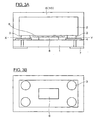
- the resin intrudes into the gaps between the functioning portions of the surface acoustic wave elements 2 and the assembly substrate 41, the functioning portions are partially covered with the resin, as shown in Figs. 3A and 3B, so that the function of the respective surface acoustic wave elements 2 is deteriorated. Thus, the produced surface acoustic wave devices may be rejected.
- Fig. 4 shows the investigation results.
- the gaps between the surface acoustic wave elements 2 and the assembly substrate 41 have a size of up to 50 ⁇ m. More preferably, the gaps have a size of up to 40 ⁇ m.
- the above-described resin-flowing-in rejection means the state in which the resin intrudes into the gaps to adhere to the functioning portions of the surface acoustic wave elements 2, and the characteristics of the surface acoustic wave device are deteriorated.
- the laminating process it is required to seal the surface acoustic wave elements 2, so that the sealing of the surface acoustic wave elements 2 can be also maintained after the cutting process which will be described below.
- the gaps between the surface acoustic wave elements 2 and the heights (thickness) of the surface acoustic wave elements 2 including the heights of the bumps are important in prevention of the formation of voids.
- the temperature (temperature of the rollers 11) at which the resin film 10 is softened and the pressure at which the resin film 10 is pressed are also important.
- the height of the surface acoustic wave element 2 means the height thereof from the surface of the assembly substrate 41.
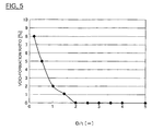
- Fig. 5 shows the investigation results.
- Fig. 5 is a graph showing the void generation ratio versus D/t.
- the expression "void generation” means that voids are formed between surface acoustic wave elements, causing the appearance to have remarkable deficiencies, or the voids cause the space under the surface acoustic wave element to be externally opened after the surface acoustic wave elements are cut to be separated (dicing), so that the sealing is insufficient. As seen in Fig.
- the amount per unit area of a resin to be supplied can be easily controlled. Relationships between design parameters, the resin-flowing-in rejection ratio, and the void generation ratio were investigated.
- the design parameters the thickness (height) d of a surface acoustic wave device (product), the volume V of the surface acoustic wave element 2 including the bumps 3 and the gap between the surface acoustic wave element 2 and the assembly substrate 41, the number n of surface acoustic wave elements per unit area on the assembly substrate 41, the thickness t1 of the resin film 10, and the average thickness t2 (cross-sectional area/length of assembly substrate) of the assembly substrate 41 are adopted.
- Fig. 6 shows the investigation results.
- Fig. 6 it has been revealed that if the following relation expressed by the formula 0.8 ⁇ d/(nV + t1 + t2) ⁇ 1.1 is established, it can be prevented that excess resin intrudes into the gaps so that the resin adheres to the functioning portions, and also, the sealing can be performed without voids being formed in the vicinities of the surface acoustic wave elements.
- the above-described formula d/(nV + t1 + t2) represents the ratio of the thickness of a surface acoustic wave device to the sum of the average height and the thicknesses of the respective members.
- the nV represents the average height (thickness) of the surface acoustic wave elements 2, calculated assuming that the surface acoustic wave elements 2 having a uniform thickness exist in the whole of the assembly substrate 41.
- the pressure is applied to the resin film 10, due to a predetermined constant gap set between the rollers 11.
- the pressure is varied, depending on the feeding speed of the assembly substrate 41 caused by the rotation of the rollers 11, the thickness of the resin film 10, and the above-described gap.
- the excess of the resin is spread in the transverse direction to flow out of the work-piece.
- the excess resin causes no problems.
- the lower limit of the feeding speed is preferably at least 0.1 m/min.
- the upper limit is up to 0.5 m/min., more preferably, up to 0.3 m/min.
- the resin film 10 can be suitably softened by controlling the rotational speed of the rollers 11, so that the large load to the assembly substrate 41 and the surface acoustic wave elements 2 can be reduced. Moreover, the thickness of the resin film 10 and the gap between the piezoelectric elements 2 and the mounting substrate 41 may be suitably adjusted so that an appropriate pressure is applied to the resin film 10. If the pressure is excessively high, the resin may intrude onto the functioning portions of the surface acoustic wave elements 2, the bumps may be broken, the surface acoustic wave elements 2 may be broken, and so forth. Thus, in such a case the produced surface acoustic wave devices have a possibility of being rejected.
- the temperatures of the rollers 11 are required to be set at values lower than the melting point of the resin film 10. If each temperature of the rollers 11 is higher than the melting point of the resin film 10, the resin film 10 becomes substantially liquid, and the fluidity is rapidly increased. This causes the resin to flow onto the functioning portions.
- the surface acoustic wave elements 2 have a pyroelectric property.
- the temperature if the temperature is rapidly increased, the electric charges accumulate on the surface acoustic wave elements 2 and discharge occurs, so that the surface acoustic wave elements 2 may be broken. Therefore, the temperature must be increased after deliberation.
- the temperature has an upper limit of 90°C and a lower limit of 30°C.
- the assembly substrate 41 is passed through between the rollers 11 in which the passing-through starts from one end of the assembly substrate 41.
- the air existing in the spaces defined by the resin film 10, the surface acoustic wave elements 2, and the assembly substrate 41 is pushed to be removed.
- the generation of voids can be prevented.
- the resin film 10 is heat-treated at a predetermined temperature, so that the resin is completely hardened as shown in process 2 of Fig.2 (hardening process). Thereby, the resin film 10 is completely hardened to function as the sealing resin 5 as shown in Fig. 1.
- the air existing between the surface acoustic wave elements 2 and the assembly substrate 41 is expanded.
- voids are formed between the surface acoustic wave elements 2.
- the sizes of the gaps between the surface acoustic wave elements 2 and the assembly substrate 41 are set to be relatively small, that is, to be less than 50 ⁇ m. Thus, the formation of voids is prevented.
- the work-piece is cut by means of a cutting unit such as a dicer or the like by a cutting-breaking method or the like, so that the respective pieces, that is, the surface acoustic wave devices, are produced (splitting process).
- a cutting unit such as a dicer or the like by a cutting-breaking method or the like
- the respective pieces that is, the surface acoustic wave devices
- the resin film 10 is heated to become a visco-elastic substance, with which the surface acoustic wave element 2 is sealed. Therefore, the surface acoustic wave element 2 can be sealed, while the adhesion of the resin to the functioning portion 6 of the surface acoustic wave element 2 is prevented.
- the sealing is hardly influenced by the warp of the assembly substrate 41 which becomes the mounting substrates 1, the conditions in which the surface acoustic wave elements 2 are mounted on the assembly substrate 41, and so forth.
- the surface acoustic wave device can be reduced in size.
- the resin film 10 since the resin film 10 is used, the resin can be applied in a constant amount in contrast to a liquid resin. Thereby, surface acoustic wave devices having stable qualities can be produced.
- the size of the gap between the surface acoustic wave elements 2 and the assembly substrate 41 which becomes the mounting substrates 1 is less than 50 ⁇ m, the amount of air existing between the surface acoustic wave elements 2 and the mounting substrate 1 can be reduced. Therefore, the formation of voids, which may be caused when the resin is hardened, can be inhibited.
- the temperature and the pressure can be applied just as required.
- pyroelectric breaking of the surface acoustic wave elements 2, the deficient connection of bumps, and breaking (chipping) of the surface acoustic wave elements 2 can be prevented.
- the pressure applied between the rollers 11 is caused by the gap between the rollers 11 which is set at a constant value.
- this method is not restrictive.
- a constant pressure may be applied in a manner which is different from the above-described method. If the pressure, caused by the gap, is excessively high, the surface acoustic wave elements 2 are broken.
- the pressure applied between the rollers 11 and 11 is up to 50 N. Moreover, it is permissible to heat only one of the rollers 11.
- the laminating process is carried out by means of the two rollers 11.
- the laminating process may be carried out as follows: the assembly substrate 41 is placed on a flat stage, followed by the laminating process using a roller applied only from the resin film 10 side.
- the assembly substrate 41 may be broken.
- the assembly substrate 41 is placed on a flat stage. Therefore, the stress applied to the assembly substrate 41 is received by the stage. Thus, the stress is inhibited from being concentrated at the assembly substrate 41. The assembly substrate 41 is prevented from being broken.
- rollers are used as jigs. This is not restrictive. Multi-stage rollers, belt rollers, and so forth may be employed. Moreover, referring to the embedding using rollers, rollers may be applied from the upper and lower sides, alternately, a roller may be applied from the upper side, while the stage is used on the lower side.
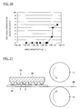
- the laminating process may be carried out as shown in Fig. 21. That is, a pre-laminate piece 14 is placed on a flat plate 60. In the pre-laminate piece 14, the resin film 10 is placed on the plural surface acoustic wave elements 2 mounted on the assembly substrate 41 via the bumps 3. The piece 14, together with the flat plate 60, is conveyed to be passed through between the two rollers 11 and 11.
- the resin film 10 is embedded along the configurations of the surface acoustic wave elements 2.
- any method may be employed, provided that the resin can be embedded while the air existing in the peripheries of the surface acoustic wave elements 2 can be pushed and removed to the outside.
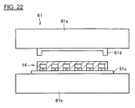
- the following method may be used: as shown in Fig. 22, the pre-laminate piece 14 is placed on a placing stage 61 c disposed on a lower side platform 61 b in a press 61; and a jig such as a press-frame 61 d fixed to the lower side of the upper-side press 61 a is descended to press the resin film 10 from the upper side thereof, so that the resin film 10 is embedded.
- a jig such as a press-frame 61 d fixed to the lower side of the upper-side press 61 a is descended to press the resin film 10 from the upper side thereof, so that the resin film 10 is embedded.
- the use of the pressing process can enhance the adhesion of the resin film 10 to the assembly substrate 41.
- the mold of the press 61 one having a frame 61 d is employed.
- the outermost periphery of the work-piece is pressed by means of the frame 61, which functions as a wall and pushes back the resin film 10 expanded due to the thermal expansion of the air.
- the frame 61 which functions as a wall and pushes back the resin film 10 expanded due to the thermal expansion of the air.
- voids can be prevented from being formed in the outermost periphery of the work-piece.
- the pressing force is set at a value at which the pressing force can counter the pressure caused by the thermal expansion of the air existing under the surface acoustic wave elements 2.
- the pressing force is determined by the press temperature. For example, when the press temperature is 150°C, the pressing force is about 0.005 kgf/mm 2 .
- the mold-frame 61d the excess of the resin flows to be removed to the outside at pressing.
- the mold-frame 61 d is effective in keeping constant the shapes of produced devices.
- the resin is hardened while it is pressed, and therefore, a sufficient adhesion can be achieved.
- the mold-frame 61 d may be provided in an integral convex mold or may be provided in a pressing surface of which the center portion is hollowed. The mold-frame 61 d may be such that it is applied to directly press the resin film 10.
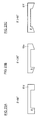
- the mold-frames 61d to 61f were prepared, in which the angles ⁇ are set at 90° (Fig. 23A), to be less than 90°, for example, at 45° (Fig. 23B), and to be more than 90°, for example, at 135° (Fig. 23C), respectively.
- the angle ⁇ is set at a value not more than 90° as in the mold-frames 61 d and 61 e. That is, it is understood that by setting the angle ⁇ at a value not more than 90°, the advantages of the pressing process described above can be sufficiently obtained, the excess of the resin can easily escape in the pressing process using the mold-frame, and thus, the formation of voids can be prevented.
- the embedding is carried out in the above-described roller process, and subsequently, the pressing process is carried out by use of a mold-frame of which the shape and the pressing-state can be finely adjusted.
- the pressing process is carried out by use of a mold-frame of which the shape and the pressing-state can be finely adjusted.
- the embedding is carried out in the roller process, and thereafter, the embedding is carried out in the laminating process.
- the embedding may be conducted in the roller process.
- the embedding may be further carried out in the roller process.
- the embedding in the press-process, that in the roller-process, and that in the press-process may be sequentially carried out.
- the embedding in the roller-process, that in the roller-process, and the press-process may be sequentially carried out.
- the assembly substrate may be broken if the pressure for embedding is high, or the embedding of the resin film 10 becomes insufficient if the pressure for embedding is too small.
- the embedding is divided and carried out several times.
- the resin film 10 may be embedded to some degree, and then, the embedding can be finely adjusted.
- the embedding can be performed at high precision.
- the surface acoustic wave elements 2 and the assembly substrate 41 can be prevented from being damaged. The generation of the above-described inconveniences can be prohibited.
- the resin film 10 after the embedding, is hardened with the shape of the resin film being maintained.
- the resin is hardened, precautions should be taken against the formation of voids which may occur due to the thermal expansion of the air existing under the surface acoustic wave elements 2.
- the resin film is forcedly pressed, and is cured while the formation of voids is prevented.
- the resin film may be fixed by means of a jig, and is directly placed in an oven to be cured.
- the work-piece since it takes much time to set the work-piece onto the jig, the work-piece may be pressed and hardened for a short time in the press-process, and is sufficiently hardened in an oven (not pressed).
- protuberances (sealing-assisting pieces) 20 are provided between the surface acoustic wave elements 2 mounted onto the assembly substrate 41.
- Protuberances 2 (sealing-assisting pieces) are provided to enhance the adhesion between the resin film and the surface acoustic wave elements 2 mounted on the assembly substrate 41 by flip-chip bonding.
- a process of forming the protuberances 20 is added to process 1 in the first embodiment. That is, the following processes 1a to 1c are employed instead of process 1.
- the protuberances 20 are formed between the positions of the assembly substrate 41 at which the surface acoustic wave elements 2 will be mounted.
- the protuberances 20 are made of metals such as gold and aluminum, resins such as polyimide, epoxy or the like, or ceramics materials, for example.
- materials having a high solid surface tension are preferred, considering the adhesion thereof to the resin film 10. Specifically, metals and ceramics materials are preferable.
- the method of forming the protuberances 20 has no particular limitation. Evaporation, sputtering, photolithography, and so forth are exemplified.
- the areas of the protuberances 20 in which the protuberances 20 themselves are bonded to the resin film 10 are as large as possible, provided that the design permits them. That is, preferably, the protuberances 20 have less tapered areas and large widths, respectively.
- the roughness of the protuberances 20 has no particular limitation. Preferably, the protuberances 20 are rather rough at the surface thereof considering the adhesion thereof to the resin film 10.
- the surface acoustic wave elements 2 are mounted onto the mounting substrate by flip chip bonding.
- the resin film 10 is placed on the surface acoustic wave elements 2 and heat-pressed, by means of jigs such as rollers or the like, to be embedded between the surface acoustic wave elements 2, as in process 1 of the first embodiment.
- process 2 the resin film 10 is hardened to function as a sealing resin.
- process 3 the work-piece is cut to be separated into respective pieces by cutting-breaking or another appropriate method by means of a cutting device such as dicer or the like.
- a cutting device such as dicer or the like.
- the protuberances 20 are formed on the assembly substrate 41.
- the resin film 10 it is not necessary to deflect the resin film 10 to a great degree.
- the gaps between the resin film 10 and the protuberances 20 are prohibited from being spread.
- the adhesion strength is enhanced.
- the resin film 10 can be made to adhere to the protuberances 20.
- the resin film 10 is fixed to high fixing strength.
- the surface acoustic wave elements 2 are securely sealed.
- the protuberances 20 are provided for the assembly substrate 41.
- the protuberances 20 function as a barrier, which prevents the resin film 10, which is hardened and bled out, from intruding into the spaces under the surface acoustic wave elements 2.
- routes in which water intrudes are reduced which provides a structure having a high moisture-proof property.
- the rigidity of the produced surface acoustic wave device is enhanced, due to the protuberances 20.
- the reliability of the surface acoustic wave device is enhanced, and the acceptance ratio of the devices is high.
- "bleed" means a phenomena in which a low molecular weight component (uncured component) contained in the resin film is oozed-out.
- the protuberances 20 are formed before the surface acoustic wave elements 2 are mounted onto the assembly substrate 41. This is not restrictive.
- the protuberances 20 may be formed after the surface acoustic wave elements 2 are mounted onto the assembly substrate 41.
- the height of the protuberances 20 the relationship between the distance h (obtained by subtracting the height of the protruberances 20 from the height (thickness) of the surface acoustic wave elements 2) and the fixing strength of the sealing resin, obtained by hot-press bonding the resin film 10 and hardening the resin, was determined. It has been revealed that preferably, the height of the protuberances 20 is larger than that of the bumps. Moreover, preferably, the height of the protuberances 20 is smaller than that (thickness) of the surface acoustic wave elements 2, considering the feasibility of the dicing. In the relationship shown in Fig.
- the height (thickness) of the surface acoustic wave elements 2 is set at 350 ⁇ m, and the height of the bumps is set at 20 ⁇ m.
- a strength obtained by pressing the side-face of the sealing resin (resin film), is measured (shear strength test).
- the side-face of the sealing resin of which the area is small, can not be pushed.
- the top side of the sealing resin (considering that the assembly substrate 41 side is "lower") is fixed by means of an adhesive or the like. Then, the side-face of the protuberances 20 in the vicinities to the surface acoustic wave elements 2 is pushed for measurement of the fixing strength.
- the protrusions may be formed by bonding a sheet having a plurality of openings onto the assembly substrate 41. That is, the sheet functions as the protuberances.
- the protuberances 20 can be easily formed.
- the surface acoustic wave elements are mounted through the openings, respectively.
- the resin film 10 is hot-press bonded, cured, and diced.
- a surface acoustic wave device is produced.
- the sheet may be bonded before or after the surface acoustic wave elements 2 are mounted onto the assembly substrate 41.
- an outer frame 21 may be provided in the periphery of the assembly substrate 41 before the resin film 10 is hot-press bonded to the assembly substrate 41, or the assembly substrate 41 may be set onto the outer frame 21.
- the outer frame 21 can prevent the resin film 10 from flowing out (being bled out). Therefore, the resin can be uniformly supplied onto the assembly substrate 41. Thereby, a surface acoustic wave device having fewer defects in appearance can be provided.
- the outer frame 21 is coated with a surface-smooth film made of a material from which the resin stuck thereto can be easily peeled off from the assembly substrate 41 after the resin film 10 is hot-press bonded.
- the material is, e.g., a fluoro-resin such as polytetrafluoroethylene or the like.
- the method of producing a surface acoustic wave device according to this embodiment is the same as that of the first or second embodiment except that the assembly substrate 41 is surface-modification-treated before or after the surface acoustic wave elements 2 are mounted onto the assembly substrate 41.
- the adhesion of the resin film 10 to the assembly substrate 41 can be enhanced.
- a sufficient fixing strength between the assembly substrate 41 and the resin film 10 can be obtained.
- the reliability of the produced surface acoustic wave device is high, and the acceptance ratio is high.
- even if the area in which the assembly substrate 41 and the resin film 10 are in contact with each other is reduced, a sufficient fixing strength can be attained.
- a surface acoustic wave device of which the size is reduced can be provided.
- the surface modification treatment for example, plasma-processing, UV processing, corona-discharge processing, excimer-laser processing, or the like may be employed.
- stains on the surface of the assembly substrate 41 can be removed therefrom, which facilitates the fixing of the resin film 10
- the surface of the assembly substrate 41 is roughened to have concavities and convexities, which facilitates the fixing, the number of OH groups at the surface, which are effective in high fixing strength, can be increased, which facilitates the fixing.
- the time required for the surface modification treatment is short, i.e., several seconds.
- the surface modification treatment will be described with reference to Fig. 11, in which the surface of the assembly substrate 41 is modified by plasma-processing after the surface acoustic wave elements 2 are mounted onto the assembly substrate 41, for example.
- the method of this embodiment is the same as that in the first embodiment except that process 1d and process 1e are used instead of process 1 in the first embodiment.
- the surface acoustic wave elements 2 are mounted onto the assembly substrate 41 by flip chip bonding.
- the surface of the assembly substrate 41 onto which the surface acoustic wave elements 2 are mounted is processed by means of plasma 40.
- process 1e the resin film 10 is arranged.
- process 2 the resin film 10 is press-bonded to the assembly substrate 41 by means of jigs such as rollers or the like.
- process 3 the resin film 10 is cured, and diced.
- a surface acoustic wave device is produced.
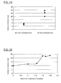
- Fig. 13 is a graph showing a relationship between the irradiation duration of the plasma 40 and the strength with which the assembly substrate 41 and the resin film 10 are fixed.
- Fig. 14 compares the fixing strengths obtained when the assembly substrate 41 is plasma-processed and when the substrate 41 is not plasma-processed. Figs. 13 and 14 evidently show that the surface-treatment of the assembly substrate 41 using the plasma 40 enhances the fixing strength.
- the solid surface tension of the assembly substrate 41 can be used as an index representing the fixing strength. As shown in Fig. 5, in the case in which the surface tension of this solid after the surface-modification-treatment is 1.2 times of that before the surface-modification-treatment, it is evaluated that the fixing strength is enhanced. That is, it is preferably that the surface tension of the solid after the surface-modification-treatment is 1.2 times of that before the treatment.
- a modification of the method of producing a surface acoustic wave device of this embodiment is illustrated in Fig.12 and includes process 1f in which the surface-modification-treatment is carried out before the surface acoustic wave elements 2 are mounted onto the assembly substrate 41, and process 1g in which the surface acoustic wave elements 2 are mounted onto the mounting substrate after the surface-modification-treatment, instead of the above-described Process 1d.
- the assembly substrate 41 can be sand-blast-processed, and primer-treated, in addition to the above-described treatment, since the assembly substrate 41 has no surface acoustic wave elements 2 mounted thereon and, clearly, no surface acoustic wave elements 2 will be broken. Thereby, the mounting strength between the surface acoustic wave elements 2 and the assembly substrate 41 (bonding of the bumps of the substrate) can be enhanced.
- the assembly substrate 41 is used for enhancement of the production efficiency, for example.
- a single surface acoustic wave element 2 may be mounted onto a mounting substrate 1, and the surface acoustic wave element 2 may be sealed with the resin film 10 according to the production process described above.
- the surface acoustic wave device suffers from the rapid change of temperature, when the device is heat-shock tested, the re-flowing is carried out, and so forth.
- the surface acoustic wave elements of the surface acoustic wave device electric charges are generated due to the pyroelectric properties of the piezoelectric substrates of the surface acoustic wave elements, when the temperature is changed as described above. With the generation of the electric charges, discharge may occur in the interdigital electrodes of the surface acoustic wave elements. As a result, the surface acoustic wave elements may be broken.
- a product is made to repeatedly go back and forth between two ovens having different temperatures, in a predetermined time, so that heat shock is applied to the product.
- the device is made to repeatedly go back and forth between ovens having temperatures of -55°C and 85°C at intervals of 30 minutes. This HS test is required by substantially all of the specifications of users.
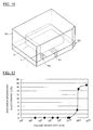
- a resin film having electro-conductivity (an electroconductive resin film) is used to form a sealing resin 50 instead of the resin film used in the arranging process in the first embodiment.
- Fig. 17 is a graph showing the investigation results. As seen in the graph, preferably, the volume resistivity of the electroconductive resin film is up to 10 10 ⁇ m.
- the surface acoustic wave device is disassembled, and it is confirmed whether the thin-film electrode (interdigital electrode) formed on the surface acoustic wave element is partially broken or not (a part of the thin-film electrode is burnt out by the spark generated during discharging).
- the electric charges generated on the piezoelectric substrates of the surface acoustic wave elements can migrateonto the resin film, so that the electric charges can be neutralized (escape). For this reason, in the surface acoustic wave device produced according to this method of this embodiment, the above-described discharge can be prohibited, and thus, breaking of the surface acoustic wave elements can be avoided.
- the electroconductive resin film may be formed as follows: a sheeting agent (thermoplastic resin) and an inorganic filler (silica gel and glass balloons) are added to an epoxy resin composition, electroconductive carbon black is added in an amount of 3 to 7% by weight, and the composition is kneaded and rolled to be formed into a sheet having a thickness of 200 ⁇ m to 500 ⁇ m.
- the conductive sheet may be formed by adding 3 to 7% by weight of conductive carbon black to a thermosetting polyimide, and forming it into a sheet having a thickness of 200 ⁇ m to 500 ⁇ m.
- the conductive resin film may be formed by forming a resin composition containing a base resin compounded with a conductive resin and a conductive material into a film.
- a base resin materials having heat-softening properties and adhesive properties may be used.
- a composition containing at least one resin selected from epoxy type resins, polyimide type resins, polyolefin resin, phenol resin and silicone resins may be employed.
- the conductive resin at least one resin selected from polypyrrole, polythiophene type resins, polyacetylene type resins, polyaniline type resins, polyphenylenevinylene type resins, and so forth may be employed.
- the conductive material at least one conductive material selected from carbon black, and metal powders of Ag, Au, Ni, and so forth may be employed. Especially, carbon black is preferable as the conductive material.
- the conductive resin film after it is hardened on the surface acoustic wave elements 2, is connected to a ground terminal (not shown) of the mounting substrate 1.
- the ground terminal may be formed on the surface (back side) of the mounting substrate 1 on which the surface acoustic wave elements 2 are not mounted.
- a side-face electrode 51 formed on the side of the mounting substrate 1, a via-hole 52 formed in the mounting substrate 1, a through-hole 53, or the like may be provided.
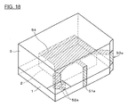
- the top surface (the surface thereof on the side opposite to the mounting surface of the surface acoustic wave element 2) of the surface acoustic wave element 2 in the package may be metallized instead of using a conductive resin film as the resin film (back-side conductive layer forming process).
- the metallizing may be performed by a dry plating process such as sputtering, evaporation, or the like, and wet-plating process using an electrolytic solution, or coating (printing) with a conductive resin, conductive paste or the like.
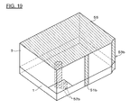
- the conductive layer 54 is formed after the mounting process described in the first embodiment. Also, preferably, the conductive layer 54 is connected to a ground terminal similarly to the sealing resin 50. For connection of the conductive layer 54 to the ground terminal, a side-face electrode 51 a formed on one side-face of the mounting substrate 1, a via-hole 52a formed in the mounting substrate 1 and the sealing resin 5, a through-hole 53a formed in the mounting substrate 1, or the like may be provided similarly to the sealing resin 50 using the conductive resin film.
- the conductive layer 54 is connected directly to the piezoelectric substrate of a surface acoustic wave element 2 on which electric charges are generated.
- the antistatic effects are high. Electric charges generated on the surface acoustic wave element 2 are rapidly neutralized by means of the conductive layer 54, and thus, discharge-breakdown can be prevented.
- the connection of the conductive layer 54 to the ground terminal ensures the discharge-breakdown preventing effects.
- only the top surface of the surface acoustic wave element 2 is metallized. The metallizing-area is small, which is advantageous in reduction of the production cost.
- the conductive layer 54 is covered with the sealing resin 5. Thus, the conductive layer 54 is prevented from being exposed to the top surface of the package on which letters are to be printed. Therefore, the color and materials for the conductive layer 54 have no limitation.
- the top-surface (the surface of the resin) of the sealing resin 5 may be metallized to form a conductive layer (surface conductive layer) 55, instead of the conductive layer 54 formed on the back-side surface of the surface acoustic wave element 2.
- the conductive layer 55 is connected to a ground terminal similarly to the sealing resin 50.
- a side-face electrode 51b is formed on an side-face of the mounting substrate 1
- a via-hole 52b is formed in the mounting substrate 1 and the sealing resin 5, or a through-hole 53b is formed in the mounting substrate 1, similarly to the sealing resin 50 using the conductive resin film.
- the conductive layer 55 neutralizes electric charges generated on the surface acoustic wave element 2, so that discharge-breakdown can be prevented.
- the connection of the conductive layer 55 to the ground terminal ensures the discharge-breakdown preventing effects.
- Fig. 20 is a graph showing the investigation results. As seen in the graph, preferably, the area-resistivities as the characteristics of the conductive layers 54 and 55 are less than 10 10 ⁇ /square.
- the surface acoustic wave device is used as a piezoelectric part, for example.
- the above-described piezoelectric part is not restrictive.
- a piezoelectric filter having piezoelectric resonators 71 to 74 arranged in a ladder-form may be used.
- each of the piezoelectric resonators 72 and 74 (which are representative of the piezoelectric resonators 71 to 74) contains an insulating film 83 over the opening 84 of a supporting substrate 82 made of silicon, and a piezoelectric thin-film 86 sandwiched between a lower electrode 85 and an upper electrode 87 from the upper and lower directions (the thickness direction of the piezoelectric thin-films 86), the piezoelectric thin film 86 being positioned so as to be on the insulating film 83 and to face the opening 84.
- a diaphragm structure 88 containing a vibrating portion can be formed, the vibrating portion comprising the piezoelectric thin film 86 sandwiched between the lower electrode 85 and the upper electrodes 87, and the insulating film 83.
- the opening 84 is formed so as to pass through the supporting substrate 82 in the thickness direction.
- the insulating film 83 is made of silicon dioxide (SiO 2 ) or alumina (Al 2 O 3 ), or has a multi-layer structure made of these substances.
- the piezoelectric thin film 86 is made of zinc oxide (ZnO), aluminum nitride (AIN), or the like.
- a concavity 84a may be formed in the supporting substrate 82 instead of the opening 84, the concavity 84a being opened so as to face the diaphragm structure and not to pass through the supporting substrate in the thickness direction.
Landscapes
- Physics & Mathematics (AREA)
- Acoustics & Sound (AREA)
- Engineering & Computer Science (AREA)
- Manufacturing & Machinery (AREA)
- Surface Acoustic Wave Elements And Circuit Networks Thereof (AREA)
- Compositions Of Oxide Ceramics (AREA)
- Transition And Organic Metals Composition Catalysts For Addition Polymerization (AREA)
- Structures Or Materials For Encapsulating Or Coating Semiconductor Devices Or Solid State Devices (AREA)
- Encapsulation Of And Coatings For Semiconductor Or Solid State Devices (AREA)
Abstract
Description
| Type of frame | Number of formed voids/evaluation-number | Determination | Remarks |
| Frame < 90° | 0/50 | Superior | = 45° |
| Frame = 90° | 1/50 | Superior | |
| Frame > 90° | 21/50 | Inferior | = 135° |
| No | 50/50 | Inferior |
- embedding in a roller process followed by embedding in a pressing process,
- embedding in a pressing process followed by embedding in a roller process,
- embedding in a roller process followed by embedding in a roller process again,
- embedding in a pressing process followed by embedding in a roller process followed by embedding in a pressing process again,
- embedding in a roller process followed by embedding in a roller process again followed by embedding in a pressing process,
Claims (34)
- A method of producing a piezoelectric part comprising the steps of:forming a piezoelectric element (2) containing a vibrating portion (6) and a bump (3) on a substrate;mounting plural piezoelectric elements (2) on a mounting substrate (1/41) having external terminals via the bumps (3) by flip chip bonding in such a manner that the vibrating portions (6) are opposed to the mounting substrate (1/41);arranging a resin film (10) on the mounting substrate (1/41) having the piezoelectric elements (2) mounted thereon;sealing the piezoelectric elements (2) by embedding the resin film (10) between neighboring piezoelectric elements mounted on the mounting substrate (1/41);hardening the resin film (10); andsplitting the mounting substrate (1/41) by dicing to take out the individual piezoelectric parts (2),the sealing step involving a step of hot-press bonding in which the resin (10) film is heated and softened, and simultaneously is pressed by means of a roller (11).
- A method of producing a piezoelectric part according to Claim 1, wherein in the step of hot-press bonding, the mounting substrate (1/41) having the piezoelectric elements (2) mounted thereon is passed through between two rollers (11).
- A method of producing a piezoelectric part according to Claim 1, wherein in the step of hot-press bonding, the mounting substrate (1/41) having the piezoelectric elements (2) mounted thereon is fixed on a flat-surface stage for the hot-press bonding.
- A method of producing a piezoelectric part according to Claim 1, wherein in the sealing step, a step of pressing the resin film (10) from the upper side thereof is carried out by use of a mold-frame (61) after the hot-press bonding step.
- A method of producing a piezoelectric part according to Claim 1, wherein in the sealing step, the hot-press bonding step is carried out by use of a mold-frame (61) after hot-press bonding step.
- A method of producing a piezoelectric part according to Claim 1, wherein in the sealing step, the hot-press bonding step is carried out again after the above-described hot-press bonding step.
- A method of producing a piezoelectric part according to Claim 1, wherein in the sealing step, after the step of pressing the resin film (10) from the upper side thereof is carried out, the hot-press bonding step and the pressing step are sequentially carried out, using the mold-frame (61).
- A method of producing a piezoelectric part according to Claim 1, wherein in the sealing step, the hot-press bonding step is carried out again after the hot-press bonding, and thereafter, the step of pressing the resin film (10) from the upper side thereof is carried out by use of the mold-frame (61).
- A method of producing a piezoelectric part according to any previous Claim, further comprising, after the arranging step, a step of disposing a resin-flowing-out preventing frame (21) on the end portion of the mounting substrate (1/41).
- A method of producing a piezoelectric part according to any previous Claim, wherein after the mounting step, a sealing-assisting piece (20) is formed between neighboring piezoelectric elements (2) mounted on the mounting substrate (1/41).
- A method of producing a piezoelectric part according to Claim 10, wherein the sealing-assisting pieces (20) are provided by bonding a sheet having plural openings to the mounting substrate (1/41).
- A method of producing a piezoelectric part according to any one of Claims 1 to 9, wherein before the mounting step, sealing assisting pieces (20) are formed between piezoelectric elements (2) mounted on the mounting substrate (1/41).
- A method of producing a piezoelectric part according to Claim 12, wherein after the sealing-assisting pieces (20) are formed, by bonding of a sheet having plural openings to the mounting substrate (1/41), piezoelectric elements (2) are mounted onto the mounting substrate (1/41) through the openings, respectively.
- A method of producing a piezoelectric part according to Claim 10 or 12, wherein the height of the sealing-assisting pieces (20) is larger than that of the bumps (3) and is smaller than that of the piezoelectric elements (2) mounted by flip chip bonding.
- A method of producing a piezoelectric part according to any previous Claim, wherein before the mounting step, the mounting substrate (1/41) is surface-modification-treated.
- A method of producing a piezoelectric part according to any one of Claims 1 to 14, wherein after the mounting step, the mounting substrate (1/41) is surface-modification-treated.
- A method of producing a piezoelectric part according to Claim 15 or 16, wherein the surface-modification-treatment is carried out by plasma-irradiation, UV-irradiation, corona-discharge, excimer-laser irradiation, or sand-blasting.
- A method of producing a piezoelectric part according to any previous Claim, wherein the distance between the piezoelectric elements (2) mounted on the mounting substrate (1/41) via the bumps (3) by flip chip bonding and the mounting substrate (1/41) is in the range of 10 µm to 50 µm.
- A method of producing a piezoelectric part according to an previous Claim, wherein the distance D between plural piezoelectric elements (2) mounted on the mounting substrate and the thickness t of the piezoelectric elements (2) involving the bumps (3) have a relationship expressed by D/t > 2.
- A method of producing a piezoelectric part according to any previous Claim 1, wherein the height d of the piezoelectric part (2), the volume V of a piezoelectric element (2) involving the bumps (3) and the distance between the piezoelectric element (2) and the mounting substrate (1/41), the number n of piezoelectric elements (2) per unit area on the mounding substrate (1/41), the thickness t1 of the resin film (10), and the average thickness t2 of the mounting substrate (1/41) (cross-sectional area/length of substrate) have a relationship expressed by 0.8 < d/(nV + t1 + t2) < 1.1.
- A method of producing a piezoelectric part according to any previous Claim, wherein the resin film (10) has a volume-resistivity of up to 1010 Ω m.
- A method of producing a piezoelectric part according to any previous Claim, further comprising a step of forming an electroconductive layer (54) on the back surface of a piezoelectric element (2) after the mounting step.
- A method of producing a piezoelectric part according to any previous Claim, further comprising a step of forming an electroconductive layer (55) on the hardened resin film (10) after the hardening step.
- A method of producing a piezoelectric part according to any previous Claim, wherein the piezoelectric element (2) is a surface acoustic wave element having at least one interdigital electrode on the surface of a piezoelectric substrate.
- A method of producing a piezoelectric part according to any one of Claims 1 to 23, wherein the piezoelectric element (2) is a piezoelectric thin-film element comprising a substrate having an opening or concavity (88), and a vibrating portion having a structure in which a piezoelectric thin-film (86) having at least one layer is sandwiched between a pair of upper and lower electrodes (85,87) opposed to each other, the vibrating portion being positioned over the opening or concavity (88).
- A piezoelectric part produced according to the method of producing a piezoelectric part defined in any previous Claim.
- A piezoelectric part comprising a piezoelectric element (2) having a vibrating portion (6) formed on the surface of a substrate;
a mounting substrate (1/41) having an external terminal (7), and onto which the piezoelectric element (2) is mounted by flip chip bonding via a bump (3) while the surface of the piezoelectric element (2) on which the vibrating portion (6) is formed is opposed to the mounting substrate (1/41); and
a resin (5/10) sealing the piezoelectric element mounted onto the mounting substrate,
the resin (5/10) having a volume resistivity of up to 1010 Ω m. - A piezoelectric part comprising a piezoelectric element (2) having a vibrating portion (6) formed on the surface of a substrate;
a mounting substrate (1/41) having an external terminal (7) and onto which the piezoelectric element (2) is mounted by flip chip bonding via a bump (3) while the surface of the piezoelectric element (2) on which the vibrating portion (6) is formed is opposed to the mounting substrate (1/41); and
a resin (5/10) sealing the piezoelectric element (2) mounted onto the mounting substrate (1/41),
the piezoelectric element (2) having a back-surface conductive layer (54) formed on the back surface thereof. - A piezoelectric part comprising a piezoelectric element (2) having a vibrating portion (6) formed on the surface of a substrate;
a mounting substrate (1/41) having an external terminal (7) and onto which the piezoelectric element (2) is mounted by flip chip bonding via a bump (3) while the surface of the piezoelectric element (2) on which the vibrating portion (6) is formed is opposed to the mounting substrate (1/41); and
a resin (5/10) sealing the piezoelectric element (2) mounted onto the mounting substrate (1/41),
the resin (5/10) having a surface conductive layer (55) formed thereon. - A piezoelectric part according to Claim 28 or 29, wherein at least one of the back-surface conductive layer (54) and the surface conductive layer (55) has an area-resistivity of up to 1010 Ω/square.
- A piezoelectric part according to Claim 28 or 29, wherein the resin (5/10) has a volume-resistivity of up to 1010 Ω m.
- A piezoelectric part according to any one of Claims 28 to 31, wherein the back-surface conductive layer (54) or the surface conductive layer (55) is connected to a ground terminal which is an external terminal of the mounting substrate (1/41).
- A method of producing a surface acoustic wave device comprising the steps of:forming a surface acoustic wave element (2) containing at least one interdigital electrode and a bump (3) formed on the surface of a piezoelectric substrate;mounting plural surface acoustic wave elements (2) on a mounting substrate (1/41) having external terminals (7) via the bumps (3) by flip chip bonding in such a manner that the interdigital electrodes are opposed to the mounting substrate (1/41);arranging a resin film (10) on the mounting substrate (1/41) having the surface acoustic wave elements (2) mounted thereon;sealing the surface acoustic wave elements (2) by embedding the resin film (10) between neighboring surface acoustic wave elements mounted on the mounting substrate (1/41);hardening the resin film (10); andsplitting the mounting substrate (1/41) by dicing to take out the individual surface acoustic wave devices.
- A method of producing a surface acoustic wave device according to Claim 33, wherein the sealing step is a hot-press bonding step in which the resin film (10) is heated to be softened, and simultaneously pressed by use of a jig.
Applications Claiming Priority (4)
| Application Number | Priority Date | Filing Date | Title |
|---|---|---|---|
| JP2002354712 | 2002-12-06 | ||
| JP2002354712 | 2002-12-06 | ||
| JP2003378190A JP2004201285A (en) | 2002-12-06 | 2003-11-07 | Method of manufacturing piezoelectric component and piezoelectric component |
| JP2003378190 | 2003-11-07 |
Publications (3)
| Publication Number | Publication Date |
|---|---|
| EP1427032A2 true EP1427032A2 (en) | 2004-06-09 |
| EP1427032A3 EP1427032A3 (en) | 2006-01-11 |
| EP1427032B1 EP1427032B1 (en) | 2008-07-30 |
Family
ID=32314128
Family Applications (1)
| Application Number | Title | Priority Date | Filing Date |
|---|---|---|---|
| EP20030293044 Expired - Lifetime EP1427032B1 (en) | 2002-12-06 | 2003-12-05 | Method of producing a piezoelectric part |
Country Status (7)
| Country | Link |
|---|---|
| US (1) | US7261792B2 (en) |
| EP (1) | EP1427032B1 (en) |
| JP (1) | JP2004201285A (en) |
| KR (1) | KR100561319B1 (en) |
| CN (1) | CN1323487C (en) |
| AT (1) | ATE403237T1 (en) |
| DE (1) | DE60322496D1 (en) |
Cited By (4)
| Publication number | Priority date | Publication date | Assignee | Title |
|---|---|---|---|---|
| WO2007067453A3 (en) * | 2005-12-07 | 2007-08-30 | Honeywell Int Inc | Surface acoustic wave pressure sensors |
| WO2012007252A1 (en) * | 2010-07-12 | 2012-01-19 | Epcos Ag | Module package and production method |
| EP2894953A4 (en) * | 2012-09-10 | 2016-07-13 | Meiko Electronics Co Ltd | Embedded printed circuit board and method for manufacturing same |
| CN114868266A (en) * | 2020-01-10 | 2022-08-05 | 日本碍子株式会社 | Piezoelectric vibration substrate and piezoelectric vibration element |
Families Citing this family (31)
| Publication number | Priority date | Publication date | Assignee | Title |
|---|---|---|---|---|
| JP3912348B2 (en) * | 2003-09-16 | 2007-05-09 | エプソントヨコム株式会社 | Manufacturing method of surface acoustic wave device |
| US7248133B2 (en) * | 2004-06-28 | 2007-07-24 | Kyocera Corporation | Method for manufacturing surface acoustic wave device |
| JP4608993B2 (en) * | 2004-08-06 | 2011-01-12 | ソニー株式会社 | Micro electromechanical element, method for manufacturing the same, and electronic apparatus |
| US7506813B2 (en) * | 2005-01-06 | 2009-03-24 | Quad/Graphics, Inc. | Resonator use in the print field |
| JP2007208568A (en) * | 2006-01-31 | 2007-08-16 | Nippon Dempa Kogyo Co Ltd | Surface mount crystal oscillator |
| US7331236B2 (en) * | 2006-03-21 | 2008-02-19 | Radi Medical Systems Ab | Pressure sensor |
| JP2009010942A (en) * | 2007-05-29 | 2009-01-15 | Nippon Dempa Kogyo Co Ltd | Piezoelectric component and manufacturing method thereof |
| JP4324811B2 (en) * | 2007-06-28 | 2009-09-02 | エプソントヨコム株式会社 | Piezoelectric vibrator and manufacturing method thereof |
| JP5264281B2 (en) * | 2008-05-09 | 2013-08-14 | 日本電波工業株式会社 | Method for manufacturing piezoelectric component |
| JP4843012B2 (en) * | 2008-11-17 | 2011-12-21 | 日本電波工業株式会社 | Piezoelectric device and manufacturing method thereof |
| TWI485825B (en) * | 2009-07-28 | 2015-05-21 | 精材科技股份有限公司 | Chip package and method of forming same |
| JP2012010054A (en) * | 2010-06-24 | 2012-01-12 | Ngk Insulators Ltd | Composite substrate and elastic wave device using thereof |
| CN102097340A (en) * | 2010-12-14 | 2011-06-15 | 沈阳中光电子有限公司 | Method for manufacturing SMD (surface mounted device) by COB (chip on board) glue filling and encapsulating |
| US10658633B2 (en) * | 2011-02-16 | 2020-05-19 | Panasonic Intellectual Property Management Co., Ltd. | Battery and manufacturing method of the battery |
| EP2852970B1 (en) * | 2012-05-22 | 2021-01-06 | Würth Elektronik GmbH & Co. KG | Method for producing an electronic subassembly |
| JP2014083281A (en) * | 2012-10-25 | 2014-05-12 | Seiko Epson Corp | Ultrasonic measuring device, head unit, probe, and diagnostic system |
| JP6205704B2 (en) * | 2012-10-25 | 2017-10-04 | セイコーエプソン株式会社 | Ultrasonic measuring device, head unit, probe and diagnostic device |
| JP2017011592A (en) * | 2015-06-24 | 2017-01-12 | 株式会社ディスコ | Manufacturing method of saw device |
| JP2018085705A (en) * | 2016-11-25 | 2018-05-31 | 太陽誘電株式会社 | Electronic component and manufacturing method thereof |
| JP6704359B2 (en) * | 2017-01-10 | 2020-06-03 | 三菱電機株式会社 | Power semiconductor device |
| JP2019125871A (en) | 2018-01-12 | 2019-07-25 | 株式会社村田製作所 | Acoustic wave device |
| CN108598254A (en) * | 2018-04-19 | 2018-09-28 | 嘉盛半导体(苏州)有限公司 | Filter package method and encapsulating structure |
| JP7180555B2 (en) * | 2019-07-02 | 2022-11-30 | 株式会社村田製作所 | Electronic component manufacturing method and electronic component manufacturing apparatus |
| CN111327226B (en) * | 2020-03-11 | 2021-09-21 | 中国科学院兰州化学物理研究所 | Method for improving energy conversion efficiency of ultrasonic motor |
| JP7508083B2 (en) * | 2020-03-25 | 2024-07-01 | 三安ジャパンテクノロジー株式会社 | Acoustic wave device package and module including an acoustic wave device |
| CN115485980B (en) * | 2020-04-24 | 2025-03-25 | 株式会社村田制作所 | High frequency module and communication device |
| KR102459794B1 (en) * | 2020-05-25 | 2022-10-28 | 이주호 | Method for forming EMI shield structure of semiconductor package |
| CN112583375A (en) * | 2020-12-15 | 2021-03-30 | 北京航天微电科技有限公司 | Method for packaging film bulk acoustic wave filter and packaging device |
| CN113436980A (en) * | 2021-06-23 | 2021-09-24 | 南昌黑鲨科技有限公司 | Device packaging method and packaging structure packaged by applying packaging method |
| US11729915B1 (en) | 2022-03-22 | 2023-08-15 | Tactotek Oy | Method for manufacturing a number of electrical nodes, electrical node module, electrical node, and multilayer structure |
| JP2024004311A (en) * | 2022-06-28 | 2024-01-16 | 三安ジャパンテクノロジー株式会社 | elastic wave device |
Family Cites Families (37)
| Publication number | Priority date | Publication date | Assignee | Title |
|---|---|---|---|---|
| US11857A (en) * | 1854-10-31 | Apparatus for tempering and flattening saws | ||
| JPS5179342A (en) * | 1974-12-26 | 1976-07-10 | Fuji Photo Film Co Ltd | |
| JPS61295025A (en) * | 1985-06-25 | 1986-12-25 | Mitsubishi Petrochem Co Ltd | Bonding of thin film |
| EP0500292B1 (en) * | 1991-02-21 | 1995-01-11 | MITSUI TOATSU CHEMICALS, Inc. | Heat-resistant polyimide adhesive |
| JP3207222B2 (en) * | 1991-08-29 | 2001-09-10 | 株式会社東芝 | Electronic component equipment |
| JPH07176565A (en) * | 1993-12-16 | 1995-07-14 | Casio Comput Co Ltd | Wiring board and manufacturing method thereof |
| JPH07321583A (en) | 1994-05-20 | 1995-12-08 | Kokusai Electric Co Ltd | Surface acoustic wave device and manufacturing method thereof |
| JPH08204497A (en) | 1995-01-26 | 1996-08-09 | Murata Mfg Co Ltd | Surface acoustic wave device |
| JP3825475B2 (en) | 1995-06-30 | 2006-09-27 | 株式会社 東芝 | Manufacturing method of electronic parts |
| JPH10125825A (en) | 1996-10-23 | 1998-05-15 | Nec Corp | Seal structure of chip device and method of sealing the same |
| US6228688B1 (en) * | 1997-02-03 | 2001-05-08 | Kabushiki Kaisha Toshiba | Flip-chip resin-encapsulated semiconductor device |
| JP2943764B2 (en) | 1997-05-16 | 1999-08-30 | 日本電気株式会社 | Resin sealing structure for flip-chip mounted semiconductor devices |
| DE19806818C1 (en) * | 1998-02-18 | 1999-11-04 | Siemens Matsushita Components | Method for producing an electronic component, in particular an SAW component working with acoustic surface waves |
| JPH11239037A (en) * | 1998-02-20 | 1999-08-31 | Nec Corp | Surface acoustic wave device |
| JP2000004139A (en) | 1998-06-16 | 2000-01-07 | Oki Electric Ind Co Ltd | Structure and method for sealing surface acoustic wave device |
| JP2000058593A (en) | 1998-08-03 | 2000-02-25 | Nec Corp | Mounting structure of surface acoustic wave device and mounting method thereof |
| JP3303791B2 (en) * | 1998-09-02 | 2002-07-22 | 株式会社村田製作所 | Electronic component manufacturing method |
| JP2000114918A (en) * | 1998-10-05 | 2000-04-21 | Mitsubishi Electric Corp | Surface acoustic wave device and method of manufacturing the same |
| EP1156520A4 (en) | 1999-01-29 | 2004-08-25 | Matsushita Electric Industrial Co Ltd | METHOD AND DEVICE FOR MOUNTING ELECTRONIC PARTS |
| JP2001110946A (en) * | 1999-10-05 | 2001-04-20 | Toshiba Corp | Electronic device and manufacturing method thereof |
| FR2799883B1 (en) * | 1999-10-15 | 2003-05-30 | Thomson Csf | METHOD OF ENCAPSULATING ELECTRONIC COMPONENTS |
| KR200192458Y1 (en) | 2000-01-18 | 2000-08-16 | 김영식 | Soothing machine for foot |
| TW569424B (en) * | 2000-03-17 | 2004-01-01 | Matsushita Electric Industrial Co Ltd | Module with embedded electric elements and the manufacturing method thereof |
| JP3376994B2 (en) * | 2000-06-27 | 2003-02-17 | 株式会社村田製作所 | Surface acoustic wave device and method of manufacturing the same |
| JP4049239B2 (en) * | 2000-08-30 | 2008-02-20 | Tdk株式会社 | Method for manufacturing high-frequency module component including surface acoustic wave element |
| JP2002217221A (en) * | 2001-01-23 | 2002-08-02 | Tdk Corp | Electronic device manufacturing method |
| JP2002217220A (en) * | 2001-01-23 | 2002-08-02 | Tdk Corp | Electronic device manufacturing method |
| JP2002217219A (en) | 2001-01-23 | 2002-08-02 | Tdk Corp | Electronic device manufacturing method |
| JP2002217523A (en) | 2001-01-23 | 2002-08-02 | Tdk Corp | Electronic device manufacturing method |
| JP2002330049A (en) * | 2001-04-27 | 2002-11-15 | Tdk Corp | Surface acoustic wave device and method of manufacturing the same |
| JP2003032061A (en) * | 2001-07-16 | 2003-01-31 | Toshiba Corp | Manufacturing method of surface acoustic wave device |
| JP2003283295A (en) * | 2002-03-25 | 2003-10-03 | Toshiba Corp | Surface acoustic wave device and method of manufacturing the same |
| JP4166997B2 (en) * | 2002-03-29 | 2008-10-15 | 富士通メディアデバイス株式会社 | Surface acoustic wave device mounting method and surface acoustic wave device having resin-sealed surface acoustic wave device |
| JP3702961B2 (en) * | 2002-10-04 | 2005-10-05 | 東洋通信機株式会社 | Manufacturing method of surface mount type SAW device |
| JP4173024B2 (en) * | 2003-02-14 | 2008-10-29 | 富士通メディアデバイス株式会社 | Electronic component manufacturing method and base substrate thereof |
| JP2004253839A (en) * | 2003-02-17 | 2004-09-09 | Toyo Commun Equip Co Ltd | Method of manufacturing surface mount type SAW device and surface mount type SAW device |
| JP3689414B2 (en) * | 2003-06-03 | 2005-08-31 | 東洋通信機株式会社 | Manufacturing method of surface acoustic wave device |
-
2003
- 2003-11-07 JP JP2003378190A patent/JP2004201285A/en active Pending
- 2003-12-04 KR KR20030087568A patent/KR100561319B1/en not_active Expired - Lifetime
- 2003-12-05 DE DE60322496T patent/DE60322496D1/en not_active Expired - Lifetime
- 2003-12-05 CN CNB2003101201160A patent/CN1323487C/en not_active Expired - Lifetime
- 2003-12-05 AT AT03293044T patent/ATE403237T1/en not_active IP Right Cessation
- 2003-12-05 EP EP20030293044 patent/EP1427032B1/en not_active Expired - Lifetime
- 2003-12-05 US US10/728,540 patent/US7261792B2/en not_active Expired - Lifetime
Cited By (6)
| Publication number | Priority date | Publication date | Assignee | Title |
|---|---|---|---|---|
| WO2007067453A3 (en) * | 2005-12-07 | 2007-08-30 | Honeywell Int Inc | Surface acoustic wave pressure sensors |
| US7651879B2 (en) | 2005-12-07 | 2010-01-26 | Honeywell International Inc. | Surface acoustic wave pressure sensors |
| WO2012007252A1 (en) * | 2010-07-12 | 2012-01-19 | Epcos Ag | Module package and production method |
| US9576870B2 (en) | 2010-07-12 | 2017-02-21 | Epcos Ag | Module package and production method |
| EP2894953A4 (en) * | 2012-09-10 | 2016-07-13 | Meiko Electronics Co Ltd | Embedded printed circuit board and method for manufacturing same |
| CN114868266A (en) * | 2020-01-10 | 2022-08-05 | 日本碍子株式会社 | Piezoelectric vibration substrate and piezoelectric vibration element |
Also Published As
| Publication number | Publication date |
|---|---|
| DE60322496D1 (en) | 2008-09-11 |
| KR100561319B1 (en) | 2006-03-16 |
| EP1427032A3 (en) | 2006-01-11 |
| ATE403237T1 (en) | 2008-08-15 |
| US7261792B2 (en) | 2007-08-28 |
| CN1507150A (en) | 2004-06-23 |
| CN1323487C (en) | 2007-06-27 |
| US20040169444A1 (en) | 2004-09-02 |
| EP1427032B1 (en) | 2008-07-30 |
| JP2004201285A (en) | 2004-07-15 |
| KR20040049800A (en) | 2004-06-12 |
Similar Documents
| Publication | Publication Date | Title |
|---|---|---|
| EP1427032B1 (en) | Method of producing a piezoelectric part | |
| JP3702961B2 (en) | Manufacturing method of surface mount type SAW device | |
| US6777814B2 (en) | Semiconductor device | |
| US6428650B1 (en) | Cover for an optical device and method for making same | |
| US6498422B1 (en) | Electronic component such as an saw device and method for producing the same | |
| KR100782280B1 (en) | Electronic component manufacturing method | |
| US6100108A (en) | Method of fabricating electronic circuit device | |
| US6432253B1 (en) | Cover with adhesive preform and method for applying same | |
| US7259032B2 (en) | Hermetically sealing a package to include a barrier metal | |
| US7154206B2 (en) | Surface acoustic wave device and method for manufacturing same | |
| US7205705B2 (en) | Electronic component and method of producing the same | |
| US20080308223A1 (en) | Electronic component and manufacturing method thereof | |
| US5886457A (en) | Sealing structure and method of sealing electronic component | |
| EP1447845A2 (en) | Package of electronic components and method for producing the same | |
| EP0951062A2 (en) | Electronic part and manufacturing method therefor | |
| WO2008016513A1 (en) | Electrical insulating layer for metallic thermal interface material | |
| JP3912324B2 (en) | Manufacturing method of surface acoustic wave device | |
| JP2004153412A (en) | Surface acoustic wave device and manufacturing method thereof | |
| JP2004007051A (en) | Sealing member and method of manufacturing surface acoustic wave device using the same | |
| JP3912348B2 (en) | Manufacturing method of surface acoustic wave device | |
| JP2004135191A (en) | Surface mount type SAW device and manufacturing method thereof | |
| JP2004253839A (en) | Method of manufacturing surface mount type SAW device and surface mount type SAW device | |
| JP2008042430A (en) | SAW device and manufacturing method thereof |
Legal Events
| Date | Code | Title | Description |
|---|---|---|---|
| PUAI | Public reference made under article 153(3) epc to a published international application that has entered the european phase |
Free format text: ORIGINAL CODE: 0009012 |
|
| 17P | Request for examination filed |
Effective date: 20031211 |
|
| AK | Designated contracting states |
Kind code of ref document: A2 Designated state(s): AT BE BG CH CY CZ DE DK EE ES FI FR GB GR HU IE IT LI LU MC NL PT RO SE SI SK TR |
|
| AX | Request for extension of the european patent |
Extension state: AL LT LV MK |
|
| PUAL | Search report despatched |
Free format text: ORIGINAL CODE: 0009013 |
|
| AK | Designated contracting states |
Kind code of ref document: A3 Designated state(s): AT BE BG CH CY CZ DE DK EE ES FI FR GB GR HU IE IT LI LU MC NL PT RO SE SI SK TR |
|
| AX | Request for extension of the european patent |
Extension state: AL LT LV MK |
|
| AKX | Designation fees paid |
Designated state(s): AT BE BG CH CY CZ DE DK EE ES FI FR GB GR HU IE IT LI LU MC NL PT RO SE SI SK TR |
|
| 17Q | First examination report despatched |
Effective date: 20060317 |
|
| 17Q | First examination report despatched |
Effective date: 20060317 |
|
| RAP1 | Party data changed (applicant data changed or rights of an application transferred) |
Owner name: MURATA MANUFACTURING CO., LTD. |
|
| RTI1 | Title (correction) |
Free format text: METHOD OF PRODUCING A PIEZOELECTRIC PART |
|
| GRAP | Despatch of communication of intention to grant a patent |
Free format text: ORIGINAL CODE: EPIDOSNIGR1 |
|
| GRAS | Grant fee paid |
Free format text: ORIGINAL CODE: EPIDOSNIGR3 |
|
| GRAA | (expected) grant |
Free format text: ORIGINAL CODE: 0009210 |
|
| AK | Designated contracting states |
Kind code of ref document: B1 Designated state(s): AT BE BG CH CY CZ DE DK EE ES FI FR GB GR HU IE IT LI LU MC NL PT RO SE SI SK TR |
|
| REG | Reference to a national code |
Ref country code: GB Ref legal event code: FG4D |
|
| REG | Reference to a national code |
Ref country code: CH Ref legal event code: EP |
|
| REF | Corresponds to: |
Ref document number: 60322496 Country of ref document: DE Date of ref document: 20080911 Kind code of ref document: P |
|
| REG | Reference to a national code |
Ref country code: IE Ref legal event code: FG4D |
|
| PG25 | Lapsed in a contracting state [announced via postgrant information from national office to epo] |
Ref country code: PT Free format text: LAPSE BECAUSE OF FAILURE TO SUBMIT A TRANSLATION OF THE DESCRIPTION OR TO PAY THE FEE WITHIN THE PRESCRIBED TIME-LIMIT Effective date: 20081230 Ref country code: NL Free format text: LAPSE BECAUSE OF FAILURE TO SUBMIT A TRANSLATION OF THE DESCRIPTION OR TO PAY THE FEE WITHIN THE PRESCRIBED TIME-LIMIT Effective date: 20080730 Ref country code: ES Free format text: LAPSE BECAUSE OF FAILURE TO SUBMIT A TRANSLATION OF THE DESCRIPTION OR TO PAY THE FEE WITHIN THE PRESCRIBED TIME-LIMIT Effective date: 20081110 |
|
| PG25 | Lapsed in a contracting state [announced via postgrant information from national office to epo] |
Ref country code: FI Free format text: LAPSE BECAUSE OF FAILURE TO SUBMIT A TRANSLATION OF THE DESCRIPTION OR TO PAY THE FEE WITHIN THE PRESCRIBED TIME-LIMIT Effective date: 20080730 Ref country code: BG Free format text: LAPSE BECAUSE OF FAILURE TO SUBMIT A TRANSLATION OF THE DESCRIPTION OR TO PAY THE FEE WITHIN THE PRESCRIBED TIME-LIMIT Effective date: 20081030 Ref country code: SI Free format text: LAPSE BECAUSE OF FAILURE TO SUBMIT A TRANSLATION OF THE DESCRIPTION OR TO PAY THE FEE WITHIN THE PRESCRIBED TIME-LIMIT Effective date: 20080730 Ref country code: AT Free format text: LAPSE BECAUSE OF FAILURE TO SUBMIT A TRANSLATION OF THE DESCRIPTION OR TO PAY THE FEE WITHIN THE PRESCRIBED TIME-LIMIT Effective date: 20080730 |
|
| PG25 | Lapsed in a contracting state [announced via postgrant information from national office to epo] |
Ref country code: BE Free format text: LAPSE BECAUSE OF FAILURE TO SUBMIT A TRANSLATION OF THE DESCRIPTION OR TO PAY THE FEE WITHIN THE PRESCRIBED TIME-LIMIT Effective date: 20080730 |
|
| PG25 | Lapsed in a contracting state [announced via postgrant information from national office to epo] |
Ref country code: EE Free format text: LAPSE BECAUSE OF FAILURE TO SUBMIT A TRANSLATION OF THE DESCRIPTION OR TO PAY THE FEE WITHIN THE PRESCRIBED TIME-LIMIT Effective date: 20080730 Ref country code: DK Free format text: LAPSE BECAUSE OF FAILURE TO SUBMIT A TRANSLATION OF THE DESCRIPTION OR TO PAY THE FEE WITHIN THE PRESCRIBED TIME-LIMIT Effective date: 20080730 |
|
| PG25 | Lapsed in a contracting state [announced via postgrant information from national office to epo] |
Ref country code: SK Free format text: LAPSE BECAUSE OF FAILURE TO SUBMIT A TRANSLATION OF THE DESCRIPTION OR TO PAY THE FEE WITHIN THE PRESCRIBED TIME-LIMIT Effective date: 20080730 Ref country code: RO Free format text: LAPSE BECAUSE OF FAILURE TO SUBMIT A TRANSLATION OF THE DESCRIPTION OR TO PAY THE FEE WITHIN THE PRESCRIBED TIME-LIMIT Effective date: 20080730 Ref country code: CZ Free format text: LAPSE BECAUSE OF FAILURE TO SUBMIT A TRANSLATION OF THE DESCRIPTION OR TO PAY THE FEE WITHIN THE PRESCRIBED TIME-LIMIT Effective date: 20080730 |
|
| PLBE | No opposition filed within time limit |
Free format text: ORIGINAL CODE: 0009261 |
|
| STAA | Information on the status of an ep patent application or granted ep patent |
Free format text: STATUS: NO OPPOSITION FILED WITHIN TIME LIMIT |
|
| 26N | No opposition filed |
Effective date: 20090506 |
|
| PG25 | Lapsed in a contracting state [announced via postgrant information from national office to epo] |
Ref country code: MC Free format text: LAPSE BECAUSE OF NON-PAYMENT OF DUE FEES Effective date: 20081231 |
|
| REG | Reference to a national code |
Ref country code: CH Ref legal event code: PL |
|
| GBPC | Gb: european patent ceased through non-payment of renewal fee |
Effective date: 20081205 |
|
| PG25 | Lapsed in a contracting state [announced via postgrant information from national office to epo] |
Ref country code: IT Free format text: LAPSE BECAUSE OF FAILURE TO SUBMIT A TRANSLATION OF THE DESCRIPTION OR TO PAY THE FEE WITHIN THE PRESCRIBED TIME-LIMIT Effective date: 20080730 |
|
| REG | Reference to a national code |
Ref country code: IE Ref legal event code: MM4A |
|
| REG | Reference to a national code |
Ref country code: FR Ref legal event code: ST Effective date: 20090831 |
|
| PG25 | Lapsed in a contracting state [announced via postgrant information from national office to epo] |
Ref country code: CH Free format text: LAPSE BECAUSE OF NON-PAYMENT OF DUE FEES Effective date: 20081231 Ref country code: LI Free format text: LAPSE BECAUSE OF NON-PAYMENT OF DUE FEES Effective date: 20081231 Ref country code: IE Free format text: LAPSE BECAUSE OF NON-PAYMENT OF DUE FEES Effective date: 20081205 |
|
| PG25 | Lapsed in a contracting state [announced via postgrant information from national office to epo] |
Ref country code: GB Free format text: LAPSE BECAUSE OF NON-PAYMENT OF DUE FEES Effective date: 20081205 |
|
| PG25 | Lapsed in a contracting state [announced via postgrant information from national office to epo] |
Ref country code: SE Free format text: LAPSE BECAUSE OF FAILURE TO SUBMIT A TRANSLATION OF THE DESCRIPTION OR TO PAY THE FEE WITHIN THE PRESCRIBED TIME-LIMIT Effective date: 20081030 |
|
| PG25 | Lapsed in a contracting state [announced via postgrant information from national office to epo] |
Ref country code: FR Free format text: LAPSE BECAUSE OF NON-PAYMENT OF DUE FEES Effective date: 20081231 |
|
| PG25 | Lapsed in a contracting state [announced via postgrant information from national office to epo] |
Ref country code: LU Free format text: LAPSE BECAUSE OF NON-PAYMENT OF DUE FEES Effective date: 20081205 Ref country code: HU Free format text: LAPSE BECAUSE OF FAILURE TO SUBMIT A TRANSLATION OF THE DESCRIPTION OR TO PAY THE FEE WITHIN THE PRESCRIBED TIME-LIMIT Effective date: 20090131 Ref country code: CY Free format text: LAPSE BECAUSE OF FAILURE TO SUBMIT A TRANSLATION OF THE DESCRIPTION OR TO PAY THE FEE WITHIN THE PRESCRIBED TIME-LIMIT Effective date: 20080730 |
|
| PG25 | Lapsed in a contracting state [announced via postgrant information from national office to epo] |
Ref country code: TR Free format text: LAPSE BECAUSE OF FAILURE TO SUBMIT A TRANSLATION OF THE DESCRIPTION OR TO PAY THE FEE WITHIN THE PRESCRIBED TIME-LIMIT Effective date: 20080730 |
|
| PG25 | Lapsed in a contracting state [announced via postgrant information from national office to epo] |
Ref country code: GR Free format text: LAPSE BECAUSE OF FAILURE TO SUBMIT A TRANSLATION OF THE DESCRIPTION OR TO PAY THE FEE WITHIN THE PRESCRIBED TIME-LIMIT Effective date: 20081031 |
|
| REG | Reference to a national code |
Ref country code: DE Ref legal event code: R079 Ref document number: 60322496 Country of ref document: DE Free format text: PREVIOUS MAIN CLASS: H01L0041220000 Ipc: H10N0030010000 |
|
| PGFP | Annual fee paid to national office [announced via postgrant information from national office to epo] |
Ref country code: DE Payment date: 20221213 Year of fee payment: 20 |
|
| REG | Reference to a national code |
Ref country code: DE Ref legal event code: R071 Ref document number: 60322496 Country of ref document: DE |