EP1424698A2 - Cam (content addressable memory) - Vorrichtung - Google Patents
Cam (content addressable memory) - Vorrichtung Download PDFInfo
- Publication number
- EP1424698A2 EP1424698A2 EP03026973A EP03026973A EP1424698A2 EP 1424698 A2 EP1424698 A2 EP 1424698A2 EP 03026973 A EP03026973 A EP 03026973A EP 03026973 A EP03026973 A EP 03026973A EP 1424698 A2 EP1424698 A2 EP 1424698A2
- Authority
- EP
- European Patent Office
- Prior art keywords
- field effect
- bit
- cam device
- cam
- node
- Prior art date
- Legal status (The legal status is an assumption and is not a legal conclusion. Google has not performed a legal analysis and makes no representation as to the accuracy of the status listed.)
- Granted
Links
Images


Classifications
-
- G—PHYSICS
- G06—COMPUTING OR CALCULATING; COUNTING
- G06F—ELECTRIC DIGITAL DATA PROCESSING
- G06F7/00—Methods or arrangements for processing data by operating upon the order or content of the data handled
- G06F7/02—Comparing digital values
-
- G—PHYSICS
- G11—INFORMATION STORAGE
- G11C—STATIC STORES
- G11C15/00—Digital stores in which information comprising one or more characteristic parts is written into the store and in which information is read-out by searching for one or more of these characteristic parts, i.e. associative or content-addressed stores
- G11C15/04—Digital stores in which information comprising one or more characteristic parts is written into the store and in which information is read-out by searching for one or more of these characteristic parts, i.e. associative or content-addressed stores using semiconductor elements
-
- G—PHYSICS
- G06—COMPUTING OR CALCULATING; COUNTING
- G06F—ELECTRIC DIGITAL DATA PROCESSING
- G06F2207/00—Indexing scheme relating to methods or arrangements for processing data by operating upon the order or content of the data handled
- G06F2207/02—Indexing scheme relating to groups G06F7/02 - G06F7/026
- G06F2207/025—String search, i.e. pattern matching, e.g. find identical word or best match in a string
Definitions
- the present invention relates to a CAM (Content Addressable Memory) device, and in particular a CAM device for pre-decoded keywords.
- CAM Content Addressable Memory
- CMOS complementary metal-oxide-semiconductor
- CAM devices Content Addressable Memories
- a CAM The operation of a CAM according to the prior art is included With reference to Figure 3 explained below.
- IP addresses stored within a CAM array 31.
- the router receives an IP packet 32, the IP address in the array 31 is searched for. If it is found, the associated hit line 33 activated, which is an ordinary memory field 34 drives in which the port number 35 is stored.
- CAM devices have usually been made up of basic CAM cells built up, each storing a data bit and this Data bit with the respective search word bit using a Compare the comparator.
- comparators diverse alternatives are known.
- static CMOS solutions are also non-complementary or dynamic Variants which optionally also with reduced signal levels can work.
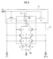
- the data bit is in a 6 transistor SRAM Cell or a cell derived from it, such as with reference to Figure 4 explains, saved.
- all data bits of equal value via an external bit line pair BL1, BL1Q connected, with both bit lines in idle state BL1, BL1Q are at a high level (precharge).
- precharge When reading, writing and comparing, one of the two bit lines BL1, BL1Q are discharged to the respective Apply data or search word bits to the cells.
- a complementary solution where the subpoena is on a low level is also used. Problematic the one that occurs above all is designed Power loss due to the constant discharging or charging of a Bit line per bit.
- the idea on which the present invention is based exists essentially in providing a CAM device which is not one bit line / comparison line per search word bit reloads, but only a bit line / comparison line for provides two search word bits.
- the comparison of two neighboring ones Data bits with the two corresponding search word bits then a common one by means of four comparison lines Comparator fed and processed there.
- the Generation of the four comparison line signals, all of them represent possible states of the two search word bits, is preferably carried out by a preprocessing device outside of the CAM array.
- Such an arrangement can be used when comparing the power loss that occurs when the bit lines are reloaded or the comparison lines occurs, are halved.
- the hit line which the Decision from n local levels to a global result summarized, can be evaluated faster, since it is only half as much many comparison results have to be processed.
- a CAM device is provided with a first storage device with a word line input, two first bit line inputs and first and second storage nodes for storage a first bit of a data word; a second storage device with one word line input, two second Bit line inputs and third and fourth storage nodes for storing a second bit of a data word; and comparator means for comparing the first and second bits with two supplied via four inputs precoded comparison bits and for driving a hit node if the first stored bit matches the first comparison bit and the second stored bit with the second comparison bit.
- the comparator device has four signal paths via three transistors each between a supply voltage and the hit node.
- the comparator device has a series parallel connection of twelve Field effect transistors of a first conductivity type.
- the comparator device has four series connections connected in parallel consisting of three field effect transistors of the first conductivity type on.
- the comparator device has a series parallel connection of eight Field effect transistors of a first conductivity type.
- the first second, third and fourth storage nodes of the storage devices such as with gate connections of two field effect transistors of the first line type of a path of the series parallel connection connected that for each of the four of 2 Bits possible bit combinations a path can be switched.
- a third transistor one of the four paths on the gate side with one of the four inputs to feed the two pre-coded ones Comparison bits connected.
- the Comparator device a field effect transistor of a second Line type with a control connection that differs from first line type differs, and lies between the hit node and a reference potential.
- the comparator device has four field effect transistors connected in series of a second line type, which differs from the first Line type differs.
- the four field effect transistors of the second conductivity type in series to a series parallel connection of field effect transistors of the first conduction type between the hit node and a reference potential.
- the Field effect transistors of the first conductivity type a P-channel and the second conduction type field effect transistors one N-channel.
- the Field effect transistors of the first conductivity type an N-channel and the second conduction type field effect transistors one P-channel.
- the comparator device has a holding device for maintaining of a signal level at the hit node.
- the holding device has three transistors on, a first and a second form an inverter, the input of which with the Hit node is connected, and its output to a gate of the third transistor is connected.
- one of the CAM device upstream circuit for generating the two Pre-coded comparison bits can be operated statically or dynamically.
- the Hit nodes are both a downstream serial Passgate hit path as well as a wired-or-hit path.
- the storage devices each constructed identically.
- the Storage devices each have six transistors, wherein four of them form two antiparallel inverters.
- a first exemplary storage device is shown in FIG. 1a 10 and a second exemplary storage device 11 are shown, which are essentially identical.
- the memory device 10 11 is one bit in each case first bit line pair BL1, BL1Q or via a second bit line pair BL2, BL2Q depending on the activation via a word line WL can be written in and read out.
- a storage device 10, 11 has six transistors, from which four form two inverters I connected in anti-parallel. The inverters I connected in antiparallel lie between a first storage node 12 and a second storage node 13, the second storage device 11 a third storage node 14 and a fourth storage node 15 of the storage device 10, 11.
- the 2-bit CAM cell is based on two static 6-transistor RAM cells 10, 11, each one bit of a stored data word take up.
- Has outputs 12, 13, 14, 15. Are not complementary Exits 13, 15 are present, so is the structure if necessary to be supplemented by an inverter I in each case in order to complement them Generate outputs.
- FIG. 1 shows a comparator device 16 which, together with the memory device 10, 11, forms a CAM device according to a first embodiment of the present invention.
- the comparator device 16 has four parallel paths, each with three P-channel field effect transistors P connected in series, between a supply voltage V V and a hit node 17 or match node 17.
- a first P-channel transistor of a first of the four parallel paths is connected to the third storage node 14 of the storage device 11.
- the gate of a second P-channel transistor P of this first path is connected to the first storage node 12 of the memory device 10, and a third P-channel transistor P in this first path is connected to a first comparison line 20.
- a second path of the four parallel paths has a first one P-channel transistor P whose gate is connected to the fourth storage node 15 of the memory device 11 is connected, wherein a second P-channel transistor P on the gate side with the first Storage node 12 of the storage device 10 is connected.
- a third P-channel field effect transistor P in this branch has a connection to a second comparison line 21 on.
- a third path of the four parallel paths indicate a first P-channel field effect transistor P on, whose gate with the third storage node 14 of the storage device 11 connected is.
- a second P-channel transistor of the third path has a gate-side connection to the second storage node 13 of the memory device 10, and a third P-channel Field effect transistor P has a connection on the gate side to a comparison line 22.
- a fourth path of the four parallel paths finally sees a first P-channel transistor P before, this one with has the fourth storage node 15 connected gate.
- a second P-channel transistor is also on the gate side the second storage node 13 of the storage device 10 in Connection, and a third P-channel transistor P has one Connection between its gate and a fourth comparison line 23 on.
- the hit node 17 can be connected via a series circuit of 4 N-channel field effect transistors N to a reference potential V M , these N-channel field effect transistors N on the gate side in each case with the first, second, third and fourth comparison lines 20, 21, 22 and 23 are connected.
- the first two P-channel transistors of the four parallel strands are consequently connected to the storage nodes 12, 13, 14 and 15 of the storage devices 10, 11, that is to say the RAM cells, in such a way that each of the four possible data bit combinations stored for two bits is representable. This interconnection ensures that at most only one of the four parallel P-channel transistor series circuits can become conductive.
- the third transistor P in each of the four parallel paths is connected to one of the corresponding precoded comparison lines 20, 21, 22, 23.
- the precoding is preferably carried out upstream, so that the first comparison line 20 is activated, e.g. provided with a signal that a corresponding connected Transistor P, N switches when the coding of the two search word bits e.g. 00 is.
- a 0 is written in the first memory device 10 as the first bit, a low level is present at the first memory node 12 and a high level is present at the second memory node 13.
- a low level is present at the third memory node 14 and a high level is present at the fourth memory node 15.
- the comparison bit pair is now also 00, then a low level is also present on the first comparison line 20 (all other comparison lines 21, 22, 23 are high) and the left outer strand is switched through, the potential at the hit Node 17 is raised to V V , ie a positive comparison result is output.
- comparison bit pair is now alternatively, for example, 01
- a low level is present on the second comparison line 21 (all other comparison lines 20, 22, 23 are high). None of the strands is switched through and the potential at the hit node 17 is not raised, ie a negative comparison result is output.
- all four comparison lines 20, 21, 22 and 23 are preferably deactivated, ie set to a high level (V V ) in the exemplary embodiment according to FIG.
- V V a high level
- the hit node 17 is consequently set to the low level (V M ) or precharged (precharge).
- the comparator device 16 detects an equality between the two bits stored in the memory device 10, 11 and the two search word bits, then the hit node 17 is reloaded to the high level (V V ) via exactly one of the four parallel P-channel transistor series connections , In the case of an inequality, however, the hit node 17 remains at the previously initiated low level.
- the comparator device 16 can, as shown in the exemplary embodiment, be supplemented by a holding device 30.
- the holding device 30 has an inverter I which is connected on the input side to the hit node 17 and at whose output there is the gate of an N-channel field-effect transistor N.
- This N-channel field effect transistor N connects the hit node 17 to the reference potential V M as long as the potential at the hit node 17 does not exceed a predetermined value.
- Figure 2a is an identical memory circuit as that with Described with reference to Figure 1a, shown.
- Figure 2 shows a reduced effort compared to Figure 1 Embodiment with only 8 P-channel transistors in Comparison to the 12 P channel transistors according to FIG. 1.
- a first path between a supply voltage V V and a hit node 17 runs via a transistor connected to the gate on the third storage node 14, a transistor connected on the gate side to the first comparison line 20 and a transistor connected on the gate side to the first storage node 12.
- a second path runs through a transistor connected to the third storage node 14 on the gate side, a transistor connected to the third comparison line 22 on the gate side and a transistor connected to the second storage node 13 on the gate side.
- a third path is provided via a P-channel transistor P, which is connected to the fourth storage node 15 on the gate side, a transistor connected to the second comparison line 21 on the gate side and a transistor P connected to the first storage node 12 on the gate side.
- a fourth path via the P-channel field effect transistor P connected to the gate on the fourth storage node 15, a transistor which is also connected on the gate side to the fourth comparison line 23 and a P-channel field effect transistor P connected to the gate on the second storage node 13.
- N is an N-channel field effect transistor N provided with a control connection 18. This single n-channel field effect transistor is turned on, if all four comparison lines 20, 21, 22, 23 are inactive are.
- the comparator can also have a complementary structure or connected, i.e. the transistors of a first one Line type e.g. P-channel transistors can by transistors of the other line type (e.g. N-channel transistors) to be replaced and vice versa.
- the hit path node 17 both a serial passgate hit path or head for a wired-or-hit path.
- the 4-way N-channel transistor series path can be replaced in any way in such a way that when all comparison lines 20, 21, 22, 23 are inactive, the hit node 17 is suitably precharged (according to FIG. 2 to potential V M ). For example, this is done via a single N-channel transistor with a separate control line 18.
- the two data bits in the storage devices 10, 11 can be any other memory structure for Come into play. Deliver the storage structures used there are no complementary outputs 13, 15, so is the comparator structure if necessary by two inverters I too expand.
Landscapes
- Physics & Mathematics (AREA)
- General Physics & Mathematics (AREA)
- Engineering & Computer Science (AREA)
- Theoretical Computer Science (AREA)
- Computational Mathematics (AREA)
- Mathematical Analysis (AREA)
- Mathematical Optimization (AREA)
- Pure & Applied Mathematics (AREA)
- General Engineering & Computer Science (AREA)
- Memory System Of A Hierarchy Structure (AREA)
- Static Random-Access Memory (AREA)
- Techniques For Improving Reliability Of Storages (AREA)
Abstract
Description
- Figur 1, 1a
- eine schematische Schaltungsanordnung zur Erläuterung einer ersten Ausführungsform der vorliegenden Erfindung, wobei Figur 1 einen erfindungsgemäßen Komparator und Figur 1a zwei exemplarische Speichereinrichtungen verdeutlicht;
- Figur 2, 2a
- eine schematische Schaltungsanordnung zur Erläuterung einer zweiten Ausführungsform der vorliegenden Erfindung, wobei Figur 2 einen erfindungsgemäßen Komparator und Figur 2a zwei exemplarische Speichereinrichtungen verdeutlicht;
- Figur 3
- ein Schaubild zur Erläuterung des bekannten CAM-Prinzips; und
- Figur 4
- eine schematische Schaltungsanordnung zur Erläuterung einer üblichen CAM-Vorrichtung.
- 10
- Speichereinrichtung
- 11
- Speichereinrichtung
- 12
- erster Speicherknoten
- 13
- zweiter Speicherknoten
- 14
- dritter Speicherknoten
- 15
- vierter Speicherknoten
- 16
- Komparatoreinrichtung
- 17
- Hit-Knoten
- 18
- Ansteuerleitung
- 20
- erste vorkodierte Vergleichsleitung
- 21
- zweite vorkodierte Vergleichsleitung
- 22
- dritte vorkodierte Vergleichsleitung
- 23
- vierte vorkodierte Vergleichsleitung
- 30
- Halteeinrichtung
- 31
- CAM-feld (content addressable memory array)
- 32
- IP-Paket
- 33
- Hit-Leitung
- 34
- Speicherfeld
- 35
- Port-Nummer
- BL1
- Bitleitung
- BL1Q
- Bitleitung mit inversem Signal zu BL1
- BL2
- Bitleitung
- BL2Q
- Bitleitung mit inversem Signal zu BL2
- VV
- Versorgungsspannung
- VM
- Bezugspotential, z.B. Masse
- N
- N-Kanal Feldeffekttransistor
- P
- P-Kanal Feldeffekttransistor
Claims (18)
- CAM (content adressable memory) -Vorrichtung mit:einer ersten Speichereinrichtung (10) mit einem Wortleitungseingang (WL) und mindestens einem Speicherknoten (12; 13) zum Speichern eines ersten Bits eines Datenwortes;einer zweiten Speichereinrichtung (11) mit einem Wortleitungseingang (WL) und mindestens einem Speicherknoten (14; 15) zum Speichern eines zweiten Bits eines Datenwortes; undeiner Komparatoreinrichtung (16) zum Vergleichen des ersten und zweiten gespeicherten Bits mit zwei über vier Eingänge (20; 21; 22; 23) zugeführten vorkodierten Vergleichsbits und zum Ansteuern eines Hit-Knoten (17) bei Übereinstimmung des ersten gespeicherten Bits mit dem ersten Vergleichsbit und des zweiten gespeicherten Bits mit dem zweiten Vergleichsbit.
- CAM- Vorrichtung nach Anspruch 1,
dadurch gekennzeichnet, dass die Komparatoreinrichtung (16) vier Signalpfade über jeweils drei Transistoren (P; N) zwischen einer Versorgungsspannung (VV) und dem Hit-Knoten (17) aufweist. - CAM- Vorrichtung nach Anspruch 2,
dadurch gekennzeichnet, dass die Komparatoreinrichtung (16) eine Reihen- Parallelschaltung aus zwölf Feldeffekttransistoren (P; N) eines ersten Leitungstyps aufweist. - CAM- Vorrichtung nach Anspruch 3,
dadurch gekennzeichnet, dass die Komparatoreinrichtung (16) vier parallel geschaltete Serienschaltungen aus jeweils drei Feldeffekttransistoren (P; N) des ersten Leitungstyps aufweist. - CAM- Vorrichtung nach Anspruch 2,
dadurch gekennzeichnet, dass die Komparatoreinrichtung (16) eine Reihen- Parallelschaltung aus acht Feldeffekttransistoren (P; N) eines ersten Leitungstyps aufweist. - CAM- Vorrichtung nach einem der vorangehenden Ansprüche 2 bis 5,
dadurch gekennzeichnet, dass ein erster, zweiter, dritter und vierter Speicherknoten (12; 13; 14; 15) der Speichereinrichtungen (10; 11) derart mit Gate- Anschlüssen eines ersten und zweiten Feldeffekttransistors (P; N) des ersten Leitungstyps jeweils eines Pfades einer Reihen- Parallelschaltung verbunden sind, daß durch jede der vier aus zwei Bits möglichen Bitkombinationen genau ein Pfad durchschaltbar ist. - CAM- Vorrichtung nach Anspruch 6,
dadurch gekennzeichnet, dass jeweils ein dritter Transistor eines der vier Pfade gate-seitig jeweils mit einem der vier Eingänge (20, 21, 22, 23) zum Zuführen der zwei vorkodierten Vergleichsbits verbunden ist. - CAM- Vorrichtung nach einem der vorangehenden Ansprüche,
dadurch gekennzeichnet, dass die Komparatoreinrichtung (16) einen Feldeffekttransistor (N; P) eines zweiten Leitungstyps mit einem Steueranschluss (18) aufweist, der sich vom ersten Leitungstyp unterscheidet, und zwischen dem Hit-Knoten (17) und einem Bezugspotential (VM) liegt. - CAM- Vorrichtung nach Anspruch 8,
dadurch gekennzeichnet, dass der Feldeffekttransistor (N; P) des zweiten Leistungstyps über den Steueranschluss (18) durchschaltbar ist, wenn alle Vergleichsleitungen (20, 21, 22, 23) einen vorbestimmten Signalpegel aufweisen. - CAM- Vorrichtung nach einem der vorangehenden Ansprüche,
dadurch gekennzeichnet, dass die Komparatoreinrichtung (16) vier in Serie geschaltete Feldeffekttransistoren (N; P) eines zweiten Leitungstyps aufweist, der sich vom ersten Leitungstyp unterscheidet. - CAM- Vorrichtung nach Anspruch 10,
dadurch gekennzeichnet, dass die vier Feldeffekttransistoren (N; P) des zweiten Leitungstyp in Serie zu einer Reihen- Parallelschaltung aus Feldeffekttransistoren (P; N) vom ersten Leitungstyp zwischen dem Hit-Knoten (17) und einem Bezugspotential (VM) liegen. - CAM- Vorrichtung nach einem der vorangehenden Ansprüche 3 bis 11,
dadurch gekennzeichnet, dass die Feldeffekttransistoren (P; N) vom ersten Leitungstyp einen p-Kanal und die Feldeffekttransistoren (N; P) vom zweiten Leitungstyp einen n-Kanal bilden. - CAM- Vorrichtung nach einem der vorangehenden Ansprüche 3 bis 11,
dadurch gekennzeichnet, dass die Feldeffekttransistoren (P; N) vom ersten Leitungstyp einen n-Kanal und die Feldeffekttransistoren (N; P) vom zweiten Leitungstyp einen p-Kanal bilden. - CAM- Vorrichtung nach einem der vorangehenden Ansprüche,
dadurch gekennzeichnet, dass die Komparatoreinrichtung (16) eine Halteeinrichtung (30) zum Aufrechterhalten eines Signalpegels an dem Hit-Knoten (17) aufweist. - CAM- Vorrichtung nach Anspruch 14,
dadurch gekennzeichnet, dass die Halteeinrichtung drei Transistoren aufweist, von denen ein erster und ein zweiter einen Inverter (I) bilden, dessen Eingang mit dem Hit-Knoten (17) verbunden ist, und dessen Ausgang an ein Gate des dritten Transistors (N; P) angeschlossen ist. - CAM- Vorrichtung nach einem der vorangehenden Ansprüche,
dadurch gekennzeichnet, dass eine der CAM- Vorrichtung vorgelagerte Schaltung zum Erzeugen der zwei vorkodierten Vergleichsbits statisch oder dynamisch betreibbar ist. - CAM- Vorrichtung nach einem der vorangehenden Ansprüche,
dadurch gekennzeichnet, dass über den Hit-Knoten (17) sowohl ein nachgelagerter Serien-Passgate-Hitpfad als auch ein Wired-Or-Hitpfad ansteuerbar ist. - CAM- Vorrichtung nach einem der vorangehenden Ansprüche,
dadurch gekennzeichnet, dass die Speichereinrichtungen (10; 11) jeweils identisch aufgebaut sind und jeweils sechs Transistoren aufweisen, wobei vier davon zwei antiparallele Inverter (I) bilden.
Applications Claiming Priority (2)
| Application Number | Priority Date | Filing Date | Title |
|---|---|---|---|
| DE10261919 | 2002-11-26 | ||
| DE10261919A DE10261919A1 (de) | 2002-11-26 | 2002-11-26 | CAM (Content Adressable Memory) - Vorrichtung |
Publications (3)
| Publication Number | Publication Date |
|---|---|
| EP1424698A2 true EP1424698A2 (de) | 2004-06-02 |
| EP1424698A3 EP1424698A3 (de) | 2006-05-24 |
| EP1424698B1 EP1424698B1 (de) | 2008-05-21 |
Family
ID=32240578
Family Applications (1)
| Application Number | Title | Priority Date | Filing Date |
|---|---|---|---|
| EP03026973A Expired - Lifetime EP1424698B1 (de) | 2002-11-26 | 2003-11-25 | Cam (content addressable memory) - Vorrichtung |
Country Status (3)
| Country | Link |
|---|---|
| US (1) | US7158396B2 (de) |
| EP (1) | EP1424698B1 (de) |
| DE (2) | DE10261919A1 (de) |
Families Citing this family (3)
| Publication number | Priority date | Publication date | Assignee | Title |
|---|---|---|---|---|
| KR101016642B1 (ko) | 2008-11-27 | 2011-02-25 | 삼성전자주식회사 | 근접 무선 통신에서의 키 관리를 위한 모바일 시스템, 서비스 시스템 및 키 인증 방법 |
| US7990743B2 (en) * | 2009-10-20 | 2011-08-02 | General Electric Company | System and method for decreasing solar collector system losses |
| US8929116B2 (en) | 2013-01-04 | 2015-01-06 | International Business Machines Corporation | Two phase search content addressable memory with power-gated main-search |
Family Cites Families (12)
| Publication number | Priority date | Publication date | Assignee | Title |
|---|---|---|---|---|
| US6000008A (en) * | 1993-03-11 | 1999-12-07 | Cabletron Systems, Inc. | Method and apparatus for matching data items of variable length in a content addressable memory |
| US5828593A (en) * | 1996-07-11 | 1998-10-27 | Northern Telecom Limited | Large-capacity content addressable memory |
| US6199140B1 (en) * | 1997-10-30 | 2001-03-06 | Netlogic Microsystems, Inc. | Multiport content addressable memory device and timing signals |
| JPH11283378A (ja) * | 1997-11-26 | 1999-10-15 | Texas Instr Inc <Ti> | 内容アドレス・メモリ |
| KR100277902B1 (ko) * | 1998-08-18 | 2001-01-15 | 김영환 | 마이크로 프로세서 |
| US5999435A (en) * | 1999-01-15 | 1999-12-07 | Fast-Chip, Inc. | Content addressable memory device |
| US6944709B2 (en) * | 1999-09-23 | 2005-09-13 | Netlogic Microsystems, Inc. | Content addressable memory with block-programmable mask write mode, word width and priority |
| US6353548B2 (en) * | 1999-12-30 | 2002-03-05 | International Business Machines Corporation | Method and data processing system for data lookups |
| EP1191540B1 (de) * | 2000-09-23 | 2006-10-04 | International Business Machines Corporation | Assoziativspeicherschaltung für Wiederauffindung in einem Datenverarbeitungssystem |
| US6421265B1 (en) * | 2001-03-22 | 2002-07-16 | Integrated Devices Technology, Inc. | DRAM-based CAM cell using 3T or 4T DRAM cells |
| DE10211957B4 (de) * | 2002-03-18 | 2007-03-08 | Infineon Technologies Ag | Ternäre inhaltsadressierbare Speicherzelle |
| US6819579B1 (en) * | 2003-04-22 | 2004-11-16 | Faraday Technology Corp. | Integrated content addressable memory architecture |
-
2002
- 2002-11-26 DE DE10261919A patent/DE10261919A1/de not_active Ceased
-
2003
- 2003-11-25 DE DE50309878T patent/DE50309878D1/de not_active Expired - Lifetime
- 2003-11-25 EP EP03026973A patent/EP1424698B1/de not_active Expired - Lifetime
- 2003-11-26 US US10/723,833 patent/US7158396B2/en not_active Expired - Lifetime
Also Published As
| Publication number | Publication date |
|---|---|
| US20040162937A1 (en) | 2004-08-19 |
| EP1424698A3 (de) | 2006-05-24 |
| DE50309878D1 (de) | 2008-07-03 |
| EP1424698B1 (de) | 2008-05-21 |
| US7158396B2 (en) | 2007-01-02 |
| DE10261919A1 (de) | 2004-06-17 |
Similar Documents
| Publication | Publication Date | Title |
|---|---|---|
| DE3041176C2 (de) | ||
| DE69827714T2 (de) | Assoziativspeichersystem | |
| DE60305208T2 (de) | Stromgesteuerter leserverstärker | |
| DE2121865C3 (de) | Speicher-Adressierschaltung | |
| DE602004001623T2 (de) | TCAM Speicher und Betriebsverfahren | |
| DE60316510T2 (de) | Inhaltsadressierbare Speicheranordnung und zugehöriges Betriebsverfahren | |
| DE69516761T2 (de) | Programmierbare hoch-geschwindigkeits schaltungsarchitektur mit geringem leistungs verbrauch | |
| DE69025297T2 (de) | Integrierte Halbleiterschaltung vom Master-slice-Typ | |
| DE3886938T2 (de) | Reprogrammierbare logische Sicherung für logische Anordnungen, basierend auf einer 6-Elementen-SRAM-Zelle. | |
| DE4018296C2 (de) | ||
| DE10155102B4 (de) | Verfahren und Vorrichtung zum Auffrischen (Refreshing) von Halbleiterspeichern | |
| DE69835116T2 (de) | Inhaltaddressierter Speicher | |
| DE69125734T2 (de) | Halbleiterspeicheranordnung | |
| DE3685889T2 (de) | Halbleiterspeicheranordnung. | |
| EP0170727B1 (de) | Integrierter Schreib-Lesespeicher | |
| DE68922738T2 (de) | Hochintegrierter Halbleiterspeicher mit Mehrfachzugang. | |
| DE69424735T2 (de) | Schaltung zum Abschalten eines Flankendetektors zum Ändern der Betriebscharakteristiken eines Speichers | |
| EP1424698B1 (de) | Cam (content addressable memory) - Vorrichtung | |
| DE10211957B4 (de) | Ternäre inhaltsadressierbare Speicherzelle | |
| DE102019201830A1 (de) | Integrierter Pegelumsetzer | |
| DE69319481T2 (de) | Zeilendekodierer zum Antreiben einer Wortleitung in mehrernpunkten | |
| DE10046051B4 (de) | Nichtflüchtiger ferroelektrischer Speicher und Schaltung zum Betreiben desselben | |
| DE60123542T2 (de) | Assoziativspeicherschaltung für Wiederauffindung in einem Datenverarbeitungssystem | |
| DE68907496T2 (de) | Dekodierer-Pufferschaltung, die in einer Halbleiterspeichereinrichtung enthalten ist. | |
| DE19507312C1 (de) | Halbleiterspeicher, dessen Speicherzellen zu einzeln adressierbaren Einheiten zusammengefaßt sind und Verfahren zum Betrieb solcher Speicher |
Legal Events
| Date | Code | Title | Description |
|---|---|---|---|
| PUAI | Public reference made under article 153(3) epc to a published international application that has entered the european phase |
Free format text: ORIGINAL CODE: 0009012 |
|
| AK | Designated contracting states |
Kind code of ref document: A2 Designated state(s): AT BE BG CH CY CZ DE DK EE ES FI FR GB GR HU IE IT LI LU MC NL PT RO SE SI SK TR |
|
| AX | Request for extension of the european patent |
Extension state: AL LT LV MK |
|
| PUAL | Search report despatched |
Free format text: ORIGINAL CODE: 0009013 |
|
| AK | Designated contracting states |
Kind code of ref document: A3 Designated state(s): AT BE BG CH CY CZ DE DK EE ES FI FR GB GR HU IE IT LI LU MC NL PT RO SE SI SK TR |
|
| AX | Request for extension of the european patent |
Extension state: AL LT LV MK |
|
| 17P | Request for examination filed |
Effective date: 20060619 |
|
| AKX | Designation fees paid |
Designated state(s): DE FR GB |
|
| 17Q | First examination report despatched |
Effective date: 20070614 |
|
| GRAP | Despatch of communication of intention to grant a patent |
Free format text: ORIGINAL CODE: EPIDOSNIGR1 |
|
| GRAS | Grant fee paid |
Free format text: ORIGINAL CODE: EPIDOSNIGR3 |
|
| GRAA | (expected) grant |
Free format text: ORIGINAL CODE: 0009210 |
|
| AK | Designated contracting states |
Kind code of ref document: B1 Designated state(s): DE FR GB |
|
| REG | Reference to a national code |
Ref country code: GB Ref legal event code: FG4D Free format text: NOT ENGLISH |
|
| REF | Corresponds to: |
Ref document number: 50309878 Country of ref document: DE Date of ref document: 20080703 Kind code of ref document: P |
|
| PLBE | No opposition filed within time limit |
Free format text: ORIGINAL CODE: 0009261 |
|
| STAA | Information on the status of an ep patent application or granted ep patent |
Free format text: STATUS: NO OPPOSITION FILED WITHIN TIME LIMIT |
|
| 26N | No opposition filed |
Effective date: 20090224 |
|
| GBPC | Gb: european patent ceased through non-payment of renewal fee |
Effective date: 20081125 |
|
| REG | Reference to a national code |
Ref country code: FR Ref legal event code: ST Effective date: 20090731 |
|
| PG25 | Lapsed in a contracting state [announced via postgrant information from national office to epo] |
Ref country code: GB Free format text: LAPSE BECAUSE OF NON-PAYMENT OF DUE FEES Effective date: 20081125 |
|
| PG25 | Lapsed in a contracting state [announced via postgrant information from national office to epo] |
Ref country code: FR Free format text: LAPSE BECAUSE OF NON-PAYMENT OF DUE FEES Effective date: 20081130 |
|
| PGFP | Annual fee paid to national office [announced via postgrant information from national office to epo] |
Ref country code: DE Payment date: 20170117 Year of fee payment: 14 |
|
| REG | Reference to a national code |
Ref country code: DE Ref legal event code: R119 Ref document number: 50309878 Country of ref document: DE |
|
| PG25 | Lapsed in a contracting state [announced via postgrant information from national office to epo] |
Ref country code: DE Free format text: LAPSE BECAUSE OF NON-PAYMENT OF DUE FEES Effective date: 20180602 |