EP1422746A2 - Monocrystalline gallium nitride localized substrate and manufacturing method thereof - Google Patents
Monocrystalline gallium nitride localized substrate and manufacturing method thereof Download PDFInfo
- Publication number
- EP1422746A2 EP1422746A2 EP03257408A EP03257408A EP1422746A2 EP 1422746 A2 EP1422746 A2 EP 1422746A2 EP 03257408 A EP03257408 A EP 03257408A EP 03257408 A EP03257408 A EP 03257408A EP 1422746 A2 EP1422746 A2 EP 1422746A2
- Authority
- EP
- European Patent Office
- Prior art keywords
- gallium nitride
- silicon
- monocrystalline
- substrate
- mask
- Prior art date
- Legal status (The legal status is an assumption and is not a legal conclusion. Google has not performed a legal analysis and makes no representation as to the accuracy of the status listed.)
- Withdrawn
Links
Images
Classifications
-
- C—CHEMISTRY; METALLURGY
- C30—CRYSTAL GROWTH
- C30B—SINGLE-CRYSTAL GROWTH; UNIDIRECTIONAL SOLIDIFICATION OF EUTECTIC MATERIAL OR UNIDIRECTIONAL DEMIXING OF EUTECTOID MATERIAL; REFINING BY ZONE-MELTING OF MATERIAL; PRODUCTION OF A HOMOGENEOUS POLYCRYSTALLINE MATERIAL WITH DEFINED STRUCTURE; SINGLE CRYSTALS OR HOMOGENEOUS POLYCRYSTALLINE MATERIAL WITH DEFINED STRUCTURE; AFTER-TREATMENT OF SINGLE CRYSTALS OR A HOMOGENEOUS POLYCRYSTALLINE MATERIAL WITH DEFINED STRUCTURE; APPARATUS THEREFOR
- C30B25/00—Single-crystal growth by chemical reaction of reactive gases, e.g. chemical vapour-deposition growth
- C30B25/02—Epitaxial-layer growth
-
- C—CHEMISTRY; METALLURGY
- C30—CRYSTAL GROWTH
- C30B—SINGLE-CRYSTAL GROWTH; UNIDIRECTIONAL SOLIDIFICATION OF EUTECTIC MATERIAL OR UNIDIRECTIONAL DEMIXING OF EUTECTOID MATERIAL; REFINING BY ZONE-MELTING OF MATERIAL; PRODUCTION OF A HOMOGENEOUS POLYCRYSTALLINE MATERIAL WITH DEFINED STRUCTURE; SINGLE CRYSTALS OR HOMOGENEOUS POLYCRYSTALLINE MATERIAL WITH DEFINED STRUCTURE; AFTER-TREATMENT OF SINGLE CRYSTALS OR A HOMOGENEOUS POLYCRYSTALLINE MATERIAL WITH DEFINED STRUCTURE; APPARATUS THEREFOR
- C30B29/00—Single crystals or homogeneous polycrystalline material with defined structure characterised by the material or by their shape
- C30B29/10—Inorganic compounds or compositions
- C30B29/40—AIIIBV compounds wherein A is B, Al, Ga, In or Tl and B is N, P, As, Sb or Bi
- C30B29/403—AIII-nitrides
- C30B29/406—Gallium nitride
-
- H—ELECTRICITY
- H10—SEMICONDUCTOR DEVICES; ELECTRIC SOLID-STATE DEVICES NOT OTHERWISE PROVIDED FOR
- H10P—GENERIC PROCESSES OR APPARATUS FOR THE MANUFACTURE OR TREATMENT OF DEVICES COVERED BY CLASS H10
- H10P14/00—Formation of materials, e.g. in the shape of layers or pillars
- H10P14/20—Formation of materials, e.g. in the shape of layers or pillars of semiconductor materials
- H10P14/27—Formation of materials, e.g. in the shape of layers or pillars of semiconductor materials using selective deposition, e.g. simultaneous growth of monocrystalline and non-monocrystalline semiconductor materials
- H10P14/271—Formation of materials, e.g. in the shape of layers or pillars of semiconductor materials using selective deposition, e.g. simultaneous growth of monocrystalline and non-monocrystalline semiconductor materials characterised by the preparation of substrate for selective deposition
-
- H—ELECTRICITY
- H10—SEMICONDUCTOR DEVICES; ELECTRIC SOLID-STATE DEVICES NOT OTHERWISE PROVIDED FOR
- H10P—GENERIC PROCESSES OR APPARATUS FOR THE MANUFACTURE OR TREATMENT OF DEVICES COVERED BY CLASS H10
- H10P14/00—Formation of materials, e.g. in the shape of layers or pillars
- H10P14/20—Formation of materials, e.g. in the shape of layers or pillars of semiconductor materials
- H10P14/29—Formation of materials, e.g. in the shape of layers or pillars of semiconductor materials characterised by the substrates
- H10P14/2901—Materials
- H10P14/2902—Materials being Group IVA materials
- H10P14/2905—Silicon, silicon germanium or germanium
-
- H—ELECTRICITY
- H10—SEMICONDUCTOR DEVICES; ELECTRIC SOLID-STATE DEVICES NOT OTHERWISE PROVIDED FOR
- H10P—GENERIC PROCESSES OR APPARATUS FOR THE MANUFACTURE OR TREATMENT OF DEVICES COVERED BY CLASS H10
- H10P14/00—Formation of materials, e.g. in the shape of layers or pillars
- H10P14/20—Formation of materials, e.g. in the shape of layers or pillars of semiconductor materials
- H10P14/32—Formation of materials, e.g. in the shape of layers or pillars of semiconductor materials characterised by intermediate layers between substrates and deposited layers
- H10P14/3202—Materials thereof
- H10P14/3204—Materials thereof being Group IVA semiconducting materials
- H10P14/3208—Silicon carbide
-
- H—ELECTRICITY
- H10—SEMICONDUCTOR DEVICES; ELECTRIC SOLID-STATE DEVICES NOT OTHERWISE PROVIDED FOR
- H10P—GENERIC PROCESSES OR APPARATUS FOR THE MANUFACTURE OR TREATMENT OF DEVICES COVERED BY CLASS H10
- H10P14/00—Formation of materials, e.g. in the shape of layers or pillars
- H10P14/20—Formation of materials, e.g. in the shape of layers or pillars of semiconductor materials
- H10P14/34—Deposited materials, e.g. layers
- H10P14/3402—Deposited materials, e.g. layers characterised by the chemical composition
- H10P14/3414—Deposited materials, e.g. layers characterised by the chemical composition being group IIIA-VIA materials
- H10P14/3416—Nitrides
Definitions
- the present invention relates to a monocrystalline gallium nitride localized substrate such that an area in which monocrystalline gallium nitride is grown is locally present on a monocrystalline silicon substrate, and to a manufacturing method thereof.
- Gallium nitride has been generally used as material for blue light-emitting elements represented by LED (light-emitting diode) and laser diode.
- LED light-emitting diode
- sapphire has been mainly used as substrates, and gallium nitride has been grown thereon by the MOCVD method.
- the following methods have been proposed: a method of integrating electronic devices and optical devices by mounting them together on the same substrate, a method of connecting plural electronic devices by optical devices, and the like.
- the former method has the problem that signal delay is inevitable due to electrical connection between the mounted electronic devices and optical devices, while the latter method has the problem that it is difficult to downsize the optical devices, and the like.
- the present invention has been created in view of the above-mentioned circumstances, and is intended for providing a monocrystalline gallium nitride localized substrate and a manufacturing method thereof, which is suitable for manufacturing electronic-optical united devices in which electronic devices and optical devices are mixedly mounted on the same silicon substrate.
- a monocrystalline gallium nitride localized substrate according to the present invention has an area in which monocrystalline gallium nitride is grown locally on a monocrystalline silicon substrate.
- a method of manufacturing a monocrystalline gallium nitride localized substrate comprises the step of forming silicon carbide on a monocrystalline silicon substrate and the step of locally forming monocrystalline gallium nitride on the above-mentioned silicon carbide, and employs silicon nitride or silicon oxide as a mask in forming the above-mentioned monocrystalline gallium nitride.
- a monocrystalline gallium nitride localized substrate according to Embodiment 1 of the present invention is manufactured in the following manner.
- silicon nitride (Si 3 N 4 ) 200 as a thin film is made to grow by the CVD method on the whole surface of a silicon substrate 100 having a face orientation (111) for film formation (refer to Fig. 1 (A)).
- This silicon nitride 200 functions as a mask in growing gallium nitride 400. That is, the gallium nitride 400 does not grow (or can be selectively removed and does not remain resultingly) in parts in which the silicon nitride 200 is formed.
- a photoresist 500 is applied on the silicon nitride 200 to superpose a photomask 600 thereon in areas in which it is undesirable to grow the gallium nitride 400, and the mask pattern is transferred by the photolithography technique (refer to Fig. 1 (B)).
- the silicon nitride 200 in parts of no photoresist 500 is removed by etching with the use of the developed photoresist 500 as a mask (refer to Fig. 1 (C)).
- the developed photoresist 500 is removed, for example by peeling it off, to expose a part 210 having no silicon nitride 200 and an island-shaped silicon nitride island 220 (refer to Fig. 1 (D)). It should be noted that the surface of the silicon substrate 100 as an initial material is exposed in the part 210 having no silicon nitride 200.
- the silicon in the part 210 having no silicon nitride 200 is modified into cubic monocrystalline silicon carbide 300 (refer to Fig. 1 (E)). Then, the face orientation of the modified monocrystalline silicon carbide 300 is (111), the same as the silicon substrate 100 initial material.
- the modification of the silicon into the monocrystalline silicon carbide 300 is performed by placing the silicon substrate 100 inside a film-forming chamber and heating the atmosphere temperature of the inside of the film-forming chamber to a temperature of 1200 to 1405°C while streaming hydrogen gas and hydrocarbon-based gas at a rate of 1 to 5 volume % with respect to the hydrogen gas as carrier gas.
- the inside of the film-forming chamber is set at atmospheric pressure.
- the hydrocarbon-based gas may be propane gas, methane gas, ethylene gas, butane gas and the like, including mixtures thereof; propane gas will be the most excellent in a high content of carbon atom and the lowest cost at the present time as compared with methane gas and ethylene gas.
- the gallium nitride 400 is made to grow epitaxially by the MOCVD method on the whole surface of the silicon substrate 100, i.e. both on the portions of silicon substrate 100 modified to monocrystalline silicon carbide 300 and the silicon nitride islands 220 (refer to Fig. 1 (F)). Then, the face orientation of the growing gallium nitride 400 is (0001). There exists a difference in crystallinity between gallium nitride 410 grown on the above-mentioned monocrystalline silicon carbide 300 and gallium nitride 420 grown on the silicon nitride island 220. The gallium nitride 410 grown on the monocrystalline silicon carbide 300 has more favorable crystallinity than the other.
- the gallium nitride 420 grown on the silicon nitride island 220 becomes polycrystalline, so as to include a great number of crystal defects and have a chemically unstable structure.
- the above-mentioned silicon nitride islands 220 are provided in areas in which it is undesirable to grow the gallium nitride 400. It is, therefore, required to remove the gallium nitride 420 grown on the silicon nitride islands 220.
- this gallium nitride 420 is performed in the following manner.
- potassium hydroxide is used as etching liquid to soak the whole sample in this etching liquid.
- This etching liquid is capable of dissolving the gallium nitride 410 grown on the monocrystalline silicon carbide 300 as well; however, the gallium nitride 420 grown on the silicon nitride islands 220 is chemically unstable, so that the etching rate thereof is higher than that of the gallium nitride 410 and consequently the gallium nitride 420 grown on the silicon nitride islands 220 is selectively etched.
- the unnecessary gallium nitride 420 can be removed with a favorable selectivity (refer to Fig. 1 (G)).
- the silicon nitride islands 220 remaining on the surface after removing the unnecessary gallium nitride 420 are etched by heated phosphoric acid to obtain a monocrystalline gallium nitride localized substrate such that the monocrystalline gallium nitride 410 is locally present (refer to Fig. 1 (H)).
- a manufacturing method of a monocrystalline gallium nitride localized substrate according to Embodiment 2 of the present invention is described referring to Fig. 2.
- This manufacturing method is as follows.
- the surface of a silicon substrate 100 having a face orientation (111) for film formation is thermally oxidized to form silicon oxide (SiO 2 ) 700 as a thin film (refer to Fig. 2 (A)).
- This silicon oxide 700 functions as a mask in growing gallium nitride 400. That is, the gallium nitride 400 does not grow (or can be selectively removed and does not remain resultingly) in parts in which the silicon oxide 700 is formed.
- a photoresist 500 is applied on the silicon oxide 700 to superpose a photomask 600 thereon in parts in which it is undesirable to grow the gallium nitride 400, and the mask pattern is transferred by the photolithography technique (refer to Fig. 2 (B)).
- the silicon oxide 700 in parts having no photoresist 500 is removed by etching with the use of the developed photoresist 500 as a mask (refer to Fig. 2 (C)).
- the developed photoresist 500 is peeled off so as to expose a part 710 having no silicon oxide 700 and an island-shaped silicon oxide island 720 (refer to Fig. 2 (D)). It should be noted that the surface of the silicon substrate 100 initial material is exposed in the part 710 having no silicon oxide 700.
- the silicon of the silicon substrate 100 exposed in the part having no silicon oxide 700 is modified into cubic monocrystalline silicon oxide 300 in the same manner as described in Embodiment 1 (refer to Fig. 2 (E)).
- the modification of the silicon into the monocrystalline silicon carbide 300 is performed in the same manner as described above, namely, by placing the silicon substrate 100 inside a film-forming chamber and heating the atmosphere temperature of the inside of the film-forming chamber to a temperature of 1200 to 1405°C while streaming hydrogen gas and hydrocarbon-based gas such as propane gas, methane gas, ethylene gas and butane gas, or mixtures of such hydrocarbon gases, at a rate of 1 to 5 volume % with respect to the hydrogen gas as carrier gas.
- the inside of the film-forming chamber is set to atmospheric pressure.
- the face orientation of the modified monocrystalline silicon carbide 300 is also (111), the same as the initial silicon substrate 100.
- the gallium nitride 400 is made to grow epitaxially by the MOCVD method on the whole silicon substrate 100, i.e. both on the portions of silicon substrate 100 modified to monocrystalline silicon carbide 300 and the silicon oxide islands 720 (refer to Fig. 2 (F)). Then, the face orientation of the growing gallium nitride 400 is (0001). There exists a difference in crystallinity between gallium nitride 410 grown on the above-mentioned monocrystalline silicon carbide 300 and gallium nitride 420 grown on the silicon oxide island 720. The gallium nitride 410 grown on the monocrystalline silicon carbide 300 has more favorable crystallinity than the other.
- the gallium nitride 420 grown on the silicon oxide island 720 includes a great number of crystal defects, so as to have a chemically unstable structure.
- the silicon oxide island 720 is provided in parts in which it is undesirable to grow the gallium nitride 400, so that it is required to remove the gallium nitride 420 grown on the silicon oxide island 720.
- this gallium nitride 420 is performed in the following manner.
- potassium hydroxide is used as etching liquid to soak the whole sample in this etching liquid.
- This etching liquid is capable of dissolving the gallium nitride 410 grown on the monocrystalline silicon carbide 300 as well; however, the gallium nitride 420 grown on the silicon oxide island 720 is chemically unstable, so that the etching rate thereof is higher than that of the gallium nitride 410 and consequently the gallium nitride 420 grown on the silicon oxide island 720 is selectively etched.
- the unnecessary gallium nitride 420 can be removed with a favorable selectivity.
- the silicon oxide island 720 remaining on the surface is etched by heated hydrofluoric acid-based etching liquid (refer to Fig. 2 (G)) to obtain a monocrystalline gallium nitride localized substrate such that the monocrystalline gallium nitride 410 is locally present (refer to Fig. 2 (H)).
- the silicon substrate 100 is used as an initial material in the above-mentioned Embodiments 1 and 2, and a monocrystalline gallium nitride localized substrate which is equivalent thereto can be manufactured also by using an SOI substrate instead through similar steps.
- a monocrystalline gallium nitride localized substrate according to the present invention locally has an area in which monocrystalline gallium nitride is grown on a monocrystalline silicon substrate.
- Such a monocrystalline gallium nitride localized substrate does not cause the problem of signal delay by forming optical devices such as LED and laser diode and electronic devices in parts thereon in which monocrystalline gallium nitride is formed and parts thereon in which monocrystalline gallium nitride is not formed respectively, as compared with products by a conventional method of sticking electronic devices and optical devices together. Also, the monocrystalline gallium nitride localized substrate can solve the problem of downsizing optical devices caused in a method of connecting electronic devices by optical devices.
Landscapes
- Chemical & Material Sciences (AREA)
- Engineering & Computer Science (AREA)
- Crystallography & Structural Chemistry (AREA)
- Materials Engineering (AREA)
- Metallurgy (AREA)
- Organic Chemistry (AREA)
- Inorganic Chemistry (AREA)
- Chemical Kinetics & Catalysis (AREA)
- General Chemical & Material Sciences (AREA)
- Crystals, And After-Treatments Of Crystals (AREA)
- Recrystallisation Techniques (AREA)
Abstract
There is provided a monocrystalline gallium
nitride localized substrate suitable for manufacturing
electronic-optical united devices in which electronic
devices and optical devices are mixedly mounted on the
same silicon substrate.
An area in which monocrystalline gallium nitride
410 is grown is locally present on a silicon substrate
100 by forming silicon carbide 200 on the silicon
substrate 100 to locally form the monocrystalline
gallium nitride 410 on the above-mentioned silicon
carbide 200. Silicon nitride 220 or silicon oxide 720
is used as a mask in forming the above-mentioned
monocrystalline gallium nitride 410.
Description
- The present invention relates to a monocrystalline gallium nitride localized substrate such that an area in which monocrystalline gallium nitride is grown is locally present on a monocrystalline silicon substrate, and to a manufacturing method thereof.
- Gallium nitride (GaN) has been generally used as material for blue light-emitting elements represented by LED (light-emitting diode) and laser diode. Conventionally, sapphire has been mainly used as substrates, and gallium nitride has been grown thereon by the MOCVD method.
- Conventionally, electronic devices represented by LSI have been formed on silicon substrates, and the input/output of signals thereof has been performed through electrodes disposed on the periphery of the package or electrodes disposed in an array state on the backside of the package.
- These days, the amount of data handled by electronic devices and operation capability required therefor have kept on an increasing course, and the demand for broader band and higher speed on signal transmission for electronic devices has been also increasing. The problem, however, is that signal delay occurs between electronic devices due to metallic wiring and parasitic capacitance occurs between transmission lines and the like. Accordingly, limitations in the improvement of performance are beginning to appear in the present situation.
- For solutions to the above-mentioned problem, the following methods have been proposed: a method of integrating electronic devices and optical devices by mounting them together on the same substrate, a method of connecting plural electronic devices by optical devices, and the like. However, the former method has the problem that signal delay is inevitable due to electrical connection between the mounted electronic devices and optical devices, while the latter method has the problem that it is difficult to downsize the optical devices, and the like.
- The present invention has been created in view of the above-mentioned circumstances, and is intended for providing a monocrystalline gallium nitride localized substrate and a manufacturing method thereof, which is suitable for manufacturing electronic-optical united devices in which electronic devices and optical devices are mixedly mounted on the same silicon substrate.
- A monocrystalline gallium nitride localized substrate according to the present invention has an area in which monocrystalline gallium nitride is grown locally on a monocrystalline silicon substrate.
- Also, a method of manufacturing a monocrystalline gallium nitride localized substrate according to the present invention comprises the step of forming silicon carbide on a monocrystalline silicon substrate and the step of locally forming monocrystalline gallium nitride on the above-mentioned silicon carbide, and employs silicon nitride or silicon oxide as a mask in forming the above-mentioned monocrystalline gallium nitride.
- Preferred embodiments of the invention will now be described by way of example only, with reference to the drawings in which:
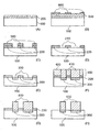
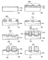
- Fig. 1 is a schematic view showing the steps of a method of manufacturing a monocrystalline gallium nitride localized substrate according to Embodiment 1 of the present invention, and Fig. 2 is a schematic view showing the steps of a method of manufacturing a monocrystalline gallium nitride localized substrate according to Embodiment 2 of the present invention.
-
-
- 100
- silicon substrate
- 200
- silicon nitride
- 300
- silicon carbide
- 400
- gallium nitride
- 500
- photoresist
- 600
- photomask
- 700
- silicon oxide
- A monocrystalline gallium nitride localized substrate according to Embodiment 1 of the present invention is manufactured in the following manner. First, silicon nitride (Si3N4) 200 as a thin film is made to grow by the CVD method on the whole surface of a
silicon substrate 100 having a face orientation (111) for film formation (refer to Fig. 1 (A)). Thissilicon nitride 200 functions as a mask in growinggallium nitride 400. That is, thegallium nitride 400 does not grow (or can be selectively removed and does not remain resultingly) in parts in which thesilicon nitride 200 is formed. - Next, a
photoresist 500 is applied on thesilicon nitride 200 to superpose aphotomask 600 thereon in areas in which it is undesirable to grow thegallium nitride 400, and the mask pattern is transferred by the photolithography technique (refer to Fig. 1 (B)). - The
silicon nitride 200 in parts of nophotoresist 500 is removed by etching with the use of thedeveloped photoresist 500 as a mask (refer to Fig. 1 (C)). Thedeveloped photoresist 500 is removed, for example by peeling it off, to expose apart 210 having nosilicon nitride 200 and an island-shaped silicon nitride island 220 (refer to Fig. 1 (D)). It should be noted that the surface of thesilicon substrate 100 as an initial material is exposed in thepart 210 having nosilicon nitride 200. - Thereafter, the silicon in the
part 210 having nosilicon nitride 200 is modified into cubic monocrystalline silicon carbide 300 (refer to Fig. 1 (E)). Then, the face orientation of the modifiedmonocrystalline silicon carbide 300 is (111), the same as thesilicon substrate 100 initial material. - The modification of the silicon into the
monocrystalline silicon carbide 300 is performed by placing thesilicon substrate 100 inside a film-forming chamber and heating the atmosphere temperature of the inside of the film-forming chamber to a temperature of 1200 to 1405°C while streaming hydrogen gas and hydrocarbon-based gas at a rate of 1 to 5 volume % with respect to the hydrogen gas as carrier gas. Also, the inside of the film-forming chamber is set at atmospheric pressure. It should be noted that the hydrocarbon-based gas may be propane gas, methane gas, ethylene gas, butane gas and the like, including mixtures thereof; propane gas will be the most excellent in a high content of carbon atom and the lowest cost at the present time as compared with methane gas and ethylene gas. - Subsequently, the
gallium nitride 400 is made to grow epitaxially by the MOCVD method on the whole surface of thesilicon substrate 100, i.e. both on the portions ofsilicon substrate 100 modified tomonocrystalline silicon carbide 300 and the silicon nitride islands 220 (refer to Fig. 1 (F)). Then, the face orientation of the growinggallium nitride 400 is (0001). There exists a difference in crystallinity betweengallium nitride 410 grown on the above-mentionedmonocrystalline silicon carbide 300 andgallium nitride 420 grown on thesilicon nitride island 220. Thegallium nitride 410 grown on themonocrystalline silicon carbide 300 has more favorable crystallinity than the other. This results from the closeness in lattice constant between the (111) face of themonocrystalline silicon carbide 300 and the (0001) face of thegallium nitride 400. On the other hand, thegallium nitride 420 grown on thesilicon nitride island 220 becomes polycrystalline, so as to include a great number of crystal defects and have a chemically unstable structure. - The above-mentioned
silicon nitride islands 220 are provided in areas in which it is undesirable to grow thegallium nitride 400. It is, therefore, required to remove thegallium nitride 420 grown on thesilicon nitride islands 220. - The removal of this
gallium nitride 420 is performed in the following manner. For example, potassium hydroxide is used as etching liquid to soak the whole sample in this etching liquid. This etching liquid is capable of dissolving thegallium nitride 410 grown on themonocrystalline silicon carbide 300 as well; however, thegallium nitride 420 grown on thesilicon nitride islands 220 is chemically unstable, so that the etching rate thereof is higher than that of thegallium nitride 410 and consequently thegallium nitride 420 grown on thesilicon nitride islands 220 is selectively etched. Thus, theunnecessary gallium nitride 420 can be removed with a favorable selectivity (refer to Fig. 1 (G)). - Next, the
silicon nitride islands 220 remaining on the surface after removing theunnecessary gallium nitride 420 are etched by heated phosphoric acid to obtain a monocrystalline gallium nitride localized substrate such that themonocrystalline gallium nitride 410 is locally present (refer to Fig. 1 (H)). - Secondly, a manufacturing method of a monocrystalline gallium nitride localized substrate according to Embodiment 2 of the present invention is described referring to Fig. 2. This manufacturing method is as follows. The surface of a
silicon substrate 100 having a face orientation (111) for film formation is thermally oxidized to form silicon oxide (SiO2) 700 as a thin film (refer to Fig. 2 (A)). Thissilicon oxide 700 functions as a mask in growinggallium nitride 400. That is, thegallium nitride 400 does not grow (or can be selectively removed and does not remain resultingly) in parts in which thesilicon oxide 700 is formed. - Next, a
photoresist 500 is applied on thesilicon oxide 700 to superpose aphotomask 600 thereon in parts in which it is undesirable to grow thegallium nitride 400, and the mask pattern is transferred by the photolithography technique (refer to Fig. 2 (B)). - The
silicon oxide 700 in parts having nophotoresist 500 is removed by etching with the use of the developedphotoresist 500 as a mask (refer to Fig. 2 (C)). The developedphotoresist 500 is peeled off so as to expose apart 710 having nosilicon oxide 700 and an island-shaped silicon oxide island 720 (refer to Fig. 2 (D)). It should be noted that the surface of thesilicon substrate 100 initial material is exposed in thepart 710 having nosilicon oxide 700. - Thereafter, the silicon of the
silicon substrate 100 exposed in the part having nosilicon oxide 700 is modified into cubicmonocrystalline silicon oxide 300 in the same manner as described in Embodiment 1 (refer to Fig. 2 (E)). The modification of the silicon into themonocrystalline silicon carbide 300 is performed in the same manner as described above, namely, by placing thesilicon substrate 100 inside a film-forming chamber and heating the atmosphere temperature of the inside of the film-forming chamber to a temperature of 1200 to 1405°C while streaming hydrogen gas and hydrocarbon-based gas such as propane gas, methane gas, ethylene gas and butane gas, or mixtures of such hydrocarbon gases, at a rate of 1 to 5 volume % with respect to the hydrogen gas as carrier gas. Also, the inside of the film-forming chamber is set to atmospheric pressure. - The face orientation of the modified
monocrystalline silicon carbide 300 is also (111), the same as theinitial silicon substrate 100. - Next, the
gallium nitride 400 is made to grow epitaxially by the MOCVD method on thewhole silicon substrate 100, i.e. both on the portions ofsilicon substrate 100 modified tomonocrystalline silicon carbide 300 and the silicon oxide islands 720 (refer to Fig. 2 (F)). Then, the face orientation of the growinggallium nitride 400 is (0001). There exists a difference in crystallinity betweengallium nitride 410 grown on the above-mentionedmonocrystalline silicon carbide 300 andgallium nitride 420 grown on thesilicon oxide island 720. Thegallium nitride 410 grown on themonocrystalline silicon carbide 300 has more favorable crystallinity than the other. This results from the closeness in lattice constant between the (111) face of themonocrystalline silicon carbide 300 and the (0001) face of thegallium nitride 400. On the other hand, thegallium nitride 420 grown on thesilicon oxide island 720 includes a great number of crystal defects, so as to have a chemically unstable structure. - The
silicon oxide island 720 is provided in parts in which it is undesirable to grow thegallium nitride 400, so that it is required to remove thegallium nitride 420 grown on thesilicon oxide island 720. - The removal of this
gallium nitride 420 is performed in the following manner. For example, potassium hydroxide is used as etching liquid to soak the whole sample in this etching liquid. This etching liquid is capable of dissolving thegallium nitride 410 grown on themonocrystalline silicon carbide 300 as well; however, thegallium nitride 420 grown on thesilicon oxide island 720 is chemically unstable, so that the etching rate thereof is higher than that of thegallium nitride 410 and consequently thegallium nitride 420 grown on thesilicon oxide island 720 is selectively etched. Thus, theunnecessary gallium nitride 420 can be removed with a favorable selectivity. - Next, the
silicon oxide island 720 remaining on the surface is etched by heated hydrofluoric acid-based etching liquid (refer to Fig. 2 (G)) to obtain a monocrystalline gallium nitride localized substrate such that themonocrystalline gallium nitride 410 is locally present (refer to Fig. 2 (H)). - It should be noted that the
silicon substrate 100 is used as an initial material in the above-mentioned Embodiments 1 and 2, and a monocrystalline gallium nitride localized substrate which is equivalent thereto can be manufactured also by using an SOI substrate instead through similar steps. - A monocrystalline gallium nitride localized substrate according to the present invention locally has an area in which monocrystalline gallium nitride is grown on a monocrystalline silicon substrate.
- Such a monocrystalline gallium nitride localized substrate does not cause the problem of signal delay by forming optical devices such as LED and laser diode and electronic devices in parts thereon in which monocrystalline gallium nitride is formed and parts thereon in which monocrystalline gallium nitride is not formed respectively, as compared with products by a conventional method of sticking electronic devices and optical devices together. Also, the monocrystalline gallium nitride localized substrate can solve the problem of downsizing optical devices caused in a method of connecting electronic devices by optical devices.
Claims (9)
- A monocrystalline gallium nitride localized substrate comprising an area of locally grown monocrystalline gallium nitride (410) on a monocrystalline silicon substrate (100).
- A monocrystalline gallium nitride localized substrate according to claim 1, wherein said monocrystalline gallium nitride is grown on silicon carbide (300) formed on the monocrystalline silicon substrate.
- A monocrystalline gallium nitride localized substrate according to claim 1 or claim 2, wherein said monocrystalline gallium nitride is grown by using silicon nitride (200) as a mask.
- A monocrystalline gallium nitride localized substrate according to claim 1 or claim 2, wherein said monocrystalline gallium nitride is grown by using silicon oxide (700) as a mask.
- A monocrystalline gallium nitride localized substrate according to any one of claims 1 to 4, wherein said monocrystalline silicon substrate is an SOI substrate.
- A method of manufacturing a monocrystalline gallium nitride localized substrate comprising the steps of:characterized in that silicon nitride (200) or silicon oxide (700) is used as a mask in forming said monocrystalline gallium nitride.forming silicon carbide (300) on a monocrystalline silicon substrate (100); andlocally forming monocrystalline gallium nitride (400) on said silicon carbide;
- A method as claimed in claim 6 wherein said mask (200, 700) of silicon nitride or silicon oxide is grown on said monocrystalline silicon substrate (100) using a CVD technique.
- A method as claimed in claim 7 wherein said mask (200, 700) of silicon nitride or silicon oxide is patterned by applying a photoresist (500) to the mask, superposing a photomask (600) on the photoresist, developing the exposed areas of the photoresist using a photolithographic technique, selectively removing the developed photoresist and selectively removing the thus-exposed areas of the mask.
- A method as claimed in claim 8 comprising:removing the undeveloped photoresist;converting the surface of the silicon substrate (100) having no mask covering to cubic monocrystalline silicon carbide;growing gallium nitride epitaxially on the whole surface of the silicon substrate including on the mask portions;selectively removing gallium nitride from the mask portions, andremoving the mask potions.
Applications Claiming Priority (2)
| Application Number | Priority Date | Filing Date | Title |
|---|---|---|---|
| JP2002341046A JP3905824B2 (en) | 2002-11-25 | 2002-11-25 | Single crystal gallium nitride localized substrate and manufacturing method thereof |
| JP2002341046 | 2002-11-25 |
Publications (1)
| Publication Number | Publication Date |
|---|---|
| EP1422746A2 true EP1422746A2 (en) | 2004-05-26 |
Family
ID=32212163
Family Applications (1)
| Application Number | Title | Priority Date | Filing Date |
|---|---|---|---|
| EP03257408A Withdrawn EP1422746A2 (en) | 2002-11-25 | 2003-11-24 | Monocrystalline gallium nitride localized substrate and manufacturing method thereof |
Country Status (6)
| Country | Link |
|---|---|
| US (2) | US20040099871A1 (en) |
| EP (1) | EP1422746A2 (en) |
| JP (1) | JP3905824B2 (en) |
| KR (1) | KR100794902B1 (en) |
| CN (1) | CN100401460C (en) |
| TW (1) | TW200425764A (en) |
Families Citing this family (10)
| Publication number | Priority date | Publication date | Assignee | Title |
|---|---|---|---|---|
| US20090261346A1 (en) * | 2008-04-16 | 2009-10-22 | Ding-Yuan Chen | Integrating CMOS and Optical Devices on a Same Chip |
| CN103031598B (en) * | 2012-08-16 | 2015-10-14 | 上海华虹宏力半导体制造有限公司 | The processing method of growing epitaxial silicon |
| US8946775B2 (en) | 2012-08-22 | 2015-02-03 | Industrial Technology Research Institute | Nitride semiconductor structure |
| JP2014078590A (en) * | 2012-10-10 | 2014-05-01 | Tokyo Electron Ltd | Semiconductor element manufacturing method and semiconductor element |
| TWI491068B (en) | 2012-11-08 | 2015-07-01 | 財團法人工業技術研究院 | Nitride semiconductor structure |
| CN104294354B (en) * | 2013-07-19 | 2016-10-19 | 上海华虹宏力半导体制造有限公司 | A kind of GaN epitaxy technique method |
| CN104538520B (en) * | 2014-12-29 | 2017-05-24 | 杭州士兰微电子股份有限公司 | Led substrate structure and manufacturing method thereof |
| US10319838B2 (en) | 2015-10-07 | 2019-06-11 | International Business Machines Corporation | III-V fin generation by lateral growth on silicon sidewall |
| CN110140209A (en) * | 2016-03-08 | 2019-08-16 | 因西亚瓦(控股)有限公司 | Indirect band gap luminescent device |
| JP7015129B2 (en) | 2017-09-11 | 2022-02-02 | 株式会社ニューフレアテクノロジー | Semiconductor devices and their manufacturing methods |
Family Cites Families (16)
| Publication number | Priority date | Publication date | Assignee | Title |
|---|---|---|---|---|
| JP3243111B2 (en) | 1993-03-15 | 2002-01-07 | 株式会社東芝 | Compound semiconductor device |
| JP3239622B2 (en) * | 1994-08-12 | 2001-12-17 | 松下電器産業株式会社 | Method of forming semiconductor thin film |
| US5563428A (en) * | 1995-01-30 | 1996-10-08 | Ek; Bruce A. | Layered structure of a substrate, a dielectric layer and a single crystal layer |
| JP3179346B2 (en) * | 1996-08-27 | 2001-06-25 | 松下電子工業株式会社 | Method for producing gallium nitride crystal |
| KR100450781B1 (en) * | 1997-08-20 | 2004-11-16 | 삼성전자주식회사 | Method for manufacturing GaN single crystal |
| KR19990062035A (en) * | 1997-12-31 | 1999-07-26 | 조장연 | Gallium Substrate Manufacturing Method Using Silicon Substrate |
| JP2927768B1 (en) | 1998-03-26 | 1999-07-28 | 技術研究組合オングストロームテクノロジ研究機構 | Semiconductor device and manufacturing method thereof |
| US6606335B1 (en) * | 1998-07-14 | 2003-08-12 | Fujitsu Limited | Semiconductor laser, semiconductor device, and their manufacture methods |
| US6255198B1 (en) * | 1998-11-24 | 2001-07-03 | North Carolina State University | Methods of fabricating gallium nitride microelectronic layers on silicon layers and gallium nitride microelectronic structures formed thereby |
| US6580098B1 (en) * | 1999-07-27 | 2003-06-17 | Toyoda Gosei Co., Ltd. | Method for manufacturing gallium nitride compound semiconductor |
| JP2001044124A (en) * | 1999-07-28 | 2001-02-16 | Sony Corp | Method of forming epitaxial layer |
| KR20010038505A (en) * | 1999-10-25 | 2001-05-15 | 남기석 | The growth of single crystal GaN on SOI structure |
| JP2001168039A (en) | 1999-12-10 | 2001-06-22 | New Japan Radio Co Ltd | Method of manufacturing semiconductor crystal grain or thin film |
| US6423983B1 (en) * | 2000-10-13 | 2002-07-23 | North Carolina State University | Optoelectronic and microelectronic devices including cubic ZnMgO and/or CdMgO alloys |
| JP4743989B2 (en) | 2000-12-15 | 2011-08-10 | 宣彦 澤木 | Semiconductor device, method for manufacturing the same, and method for manufacturing a semiconductor substrate |
| JP2002241198A (en) * | 2001-02-13 | 2002-08-28 | Hitachi Cable Ltd | GaN single crystal substrate and method of manufacturing the same |
-
2002
- 2002-11-25 JP JP2002341046A patent/JP3905824B2/en not_active Expired - Fee Related
-
2003
- 2003-10-31 TW TW092130541A patent/TW200425764A/en unknown
- 2003-11-04 US US10/699,832 patent/US20040099871A1/en not_active Abandoned
- 2003-11-07 KR KR1020030078594A patent/KR100794902B1/en not_active Expired - Fee Related
- 2003-11-24 EP EP03257408A patent/EP1422746A2/en not_active Withdrawn
- 2003-11-25 CN CNB200310119925XA patent/CN100401460C/en not_active Expired - Fee Related
-
2005
- 2005-02-14 US US11/055,985 patent/US7393763B2/en not_active Expired - Fee Related
Also Published As
| Publication number | Publication date |
|---|---|
| JP3905824B2 (en) | 2007-04-18 |
| US7393763B2 (en) | 2008-07-01 |
| US20050148108A1 (en) | 2005-07-07 |
| KR20040045300A (en) | 2004-06-01 |
| JP2004179242A (en) | 2004-06-24 |
| TW200425764A (en) | 2004-11-16 |
| CN100401460C (en) | 2008-07-09 |
| KR100794902B1 (en) | 2008-01-14 |
| US20040099871A1 (en) | 2004-05-27 |
| CN1508843A (en) | 2004-06-30 |
Similar Documents
| Publication | Publication Date | Title |
|---|---|---|
| US6100104A (en) | Method for fabricating a plurality of semiconductor bodies | |
| US8058705B2 (en) | Composite material substrate | |
| US12068166B2 (en) | Semiconductor substrate | |
| US7393763B2 (en) | Manufacturing method of monocrystalline gallium nitride localized substrate | |
| CN116529851A (en) | Epitaxial substrate, preparation method thereof and semiconductor wafer | |
| CN100505164C (en) | Method for manufacturing nitride semiconductor substrate and composite material substrate | |
| KR20040014312A (en) | Semiconductor device production method and semiconductor device | |
| US20240371669A1 (en) | Carrier substrate for semiconductor structures suitable for a transfer by transfer print and manufacturing of the semiconductor structures on the carrier substrate | |
| WO2021026872A1 (en) | Transfer method for semiconductor thin film layer and manufacturing method for composite wafer | |
| KR100454907B1 (en) | Nitride Semiconductor substrate and method for manufacturing the same | |
| KR100359739B1 (en) | Method of fusion for heteroepitaxial layers and overgrowth thereon | |
| US20070298592A1 (en) | Method for manufacturing single crystalline gallium nitride material substrate | |
| KR20050029735A (en) | Method for manufacturing thick gan layer capable of reducing defects and easily separating | |
| KR100454908B1 (en) | Method for manufacturing GaN substrate | |
| JP2706592B2 (en) | Crystal substrate manufacturing method | |
| JP2000058454A (en) | Method for forming mask for lateral epitaxial growth and method for lateral epitaxial growth | |
| JPH0258248A (en) | Manufacturing method of semiconductor device | |
| KR20230166692A (en) | Method of manufactruring piezoelectric thin film and device using the same | |
| KR930011459B1 (en) | Isolation Method of Semiconductor Devices | |
| CN115896939A (en) | Gallium nitride epitaxial substrate and preparation method thereof | |
| US20080227273A1 (en) | Method for manufacturing semiconductor device | |
| KR100425097B1 (en) | method for overgrowth GaN layer | |
| JPH04311029A (en) | Manufacture of semiconductor thin film | |
| KR20030083819A (en) | Method for manufacturing a Nitride chemical compound substrate | |
| JPH1070308A (en) | Manufacture of light-emitting diode array |
Legal Events
| Date | Code | Title | Description |
|---|---|---|---|
| PUAI | Public reference made under article 153(3) epc to a published international application that has entered the european phase |
Free format text: ORIGINAL CODE: 0009012 |
|
| AK | Designated contracting states |
Kind code of ref document: A2 Designated state(s): AT BE BG CH CY CZ DE DK EE ES FI FR GB GR HU IE IT LI LU MC NL PT RO SE SI SK TR |
|
| AX | Request for extension of the european patent |
Extension state: AL LT LV MK |
|
| STAA | Information on the status of an ep patent application or granted ep patent |
Free format text: STATUS: THE APPLICATION HAS BEEN WITHDRAWN |
|
| 18W | Application withdrawn |
Effective date: 20080731 |