EP1422311A2 - Hard film and hard film coated tool - Google Patents
Hard film and hard film coated tool Download PDFInfo
- Publication number
- EP1422311A2 EP1422311A2 EP03026508A EP03026508A EP1422311A2 EP 1422311 A2 EP1422311 A2 EP 1422311A2 EP 03026508 A EP03026508 A EP 03026508A EP 03026508 A EP03026508 A EP 03026508A EP 1422311 A2 EP1422311 A2 EP 1422311A2
- Authority
- EP
- European Patent Office
- Prior art keywords
- hard film
- hard
- film
- oxygen
- face
- Prior art date
- Legal status (The legal status is an assumption and is not a legal conclusion. Google has not performed a legal analysis and makes no representation as to the accuracy of the status listed.)
- Granted
Links
Images

Classifications
-
- C—CHEMISTRY; METALLURGY
- C23—COATING METALLIC MATERIAL; COATING MATERIAL WITH METALLIC MATERIAL; CHEMICAL SURFACE TREATMENT; DIFFUSION TREATMENT OF METALLIC MATERIAL; COATING BY VACUUM EVAPORATION, BY SPUTTERING, BY ION IMPLANTATION OR BY CHEMICAL VAPOUR DEPOSITION, IN GENERAL; INHIBITING CORROSION OF METALLIC MATERIAL OR INCRUSTATION IN GENERAL
- C23C—COATING METALLIC MATERIAL; COATING MATERIAL WITH METALLIC MATERIAL; SURFACE TREATMENT OF METALLIC MATERIAL BY DIFFUSION INTO THE SURFACE, BY CHEMICAL CONVERSION OR SUBSTITUTION; COATING BY VACUUM EVAPORATION, BY SPUTTERING, BY ION IMPLANTATION OR BY CHEMICAL VAPOUR DEPOSITION, IN GENERAL
- C23C14/00—Coating by vacuum evaporation, by sputtering or by ion implantation of the coating forming material
- C23C14/06—Coating by vacuum evaporation, by sputtering or by ion implantation of the coating forming material characterised by the coating material
- C23C14/0641—Nitrides
-
- C—CHEMISTRY; METALLURGY
- C23—COATING METALLIC MATERIAL; COATING MATERIAL WITH METALLIC MATERIAL; CHEMICAL SURFACE TREATMENT; DIFFUSION TREATMENT OF METALLIC MATERIAL; COATING BY VACUUM EVAPORATION, BY SPUTTERING, BY ION IMPLANTATION OR BY CHEMICAL VAPOUR DEPOSITION, IN GENERAL; INHIBITING CORROSION OF METALLIC MATERIAL OR INCRUSTATION IN GENERAL
- C23C—COATING METALLIC MATERIAL; COATING MATERIAL WITH METALLIC MATERIAL; SURFACE TREATMENT OF METALLIC MATERIAL BY DIFFUSION INTO THE SURFACE, BY CHEMICAL CONVERSION OR SUBSTITUTION; COATING BY VACUUM EVAPORATION, BY SPUTTERING, BY ION IMPLANTATION OR BY CHEMICAL VAPOUR DEPOSITION, IN GENERAL
- C23C14/00—Coating by vacuum evaporation, by sputtering or by ion implantation of the coating forming material
- C23C14/06—Coating by vacuum evaporation, by sputtering or by ion implantation of the coating forming material characterised by the coating material
- C23C14/0676—Oxynitrides
-
- C—CHEMISTRY; METALLURGY
- C23—COATING METALLIC MATERIAL; COATING MATERIAL WITH METALLIC MATERIAL; CHEMICAL SURFACE TREATMENT; DIFFUSION TREATMENT OF METALLIC MATERIAL; COATING BY VACUUM EVAPORATION, BY SPUTTERING, BY ION IMPLANTATION OR BY CHEMICAL VAPOUR DEPOSITION, IN GENERAL; INHIBITING CORROSION OF METALLIC MATERIAL OR INCRUSTATION IN GENERAL
- C23C—COATING METALLIC MATERIAL; COATING MATERIAL WITH METALLIC MATERIAL; SURFACE TREATMENT OF METALLIC MATERIAL BY DIFFUSION INTO THE SURFACE, BY CHEMICAL CONVERSION OR SUBSTITUTION; COATING BY VACUUM EVAPORATION, BY SPUTTERING, BY ION IMPLANTATION OR BY CHEMICAL VAPOUR DEPOSITION, IN GENERAL
- C23C30/00—Coating with metallic material characterised only by the composition of the metallic material, i.e. not characterised by the coating process
- C23C30/005—Coating with metallic material characterised only by the composition of the metallic material, i.e. not characterised by the coating process on hard metal substrates
-
- Y—GENERAL TAGGING OF NEW TECHNOLOGICAL DEVELOPMENTS; GENERAL TAGGING OF CROSS-SECTIONAL TECHNOLOGIES SPANNING OVER SEVERAL SECTIONS OF THE IPC; TECHNICAL SUBJECTS COVERED BY FORMER USPC CROSS-REFERENCE ART COLLECTIONS [XRACs] AND DIGESTS
- Y10—TECHNICAL SUBJECTS COVERED BY FORMER USPC
- Y10T—TECHNICAL SUBJECTS COVERED BY FORMER US CLASSIFICATION
- Y10T428/00—Stock material or miscellaneous articles
- Y10T428/31—Surface property or characteristic of web, sheet or block
Definitions
- the present invention relates to a hard film having excellent wear resistance, adhesion and high-temperature oxidation resistance, which is formed on cemented carbide, high-speed steel, die steel, etc., particularly to a hard film for being formed on wear-resistant members requiring high hardness such as cutting tools, forming dies, bearings, dies and rolls, and heat-resistant members such as internal combustion engine parts.
- the present invention also relates to a tool coated with such a hard film.
- this amorphous film has a Knoop hardness of about 21 GPa at most, insufficient in wear resistance and adhesion.
- Japanese Patent 3039381 discloses a method comprising generating a vapor mixture of Al and Cr from a target composed of 25-50 atomic % of Al and 75-50 atomic % of Cr disposed in a vacuum chamber by arc discharge, and simultaneously introducing a nitrogen gas into the vacuum chamber to cause a reaction between the vapor mixture and the nitrogen gas, thereby forming an Al-Cr-N composite hard film having excellent high-temperature oxidation resistance that prevents oxidation even at 800-900°C on a substrate.
- JP 2002-160129 A discloses a method for surface-treating a tool, comprising forming an intermediate layer of Ti, Cr, Si or Al on a substrate surface, and coating the intermediate layer with a hard film of AlCrN.
- These hard films are made of AlCr nitride having a high-temperature oxidation resistance of about 1000°C. However, they do not have oxidation resistance exceeding 1000°C. Further, these hard films had as insufficient hardness Hv as about 21 GPa, poor in wear resistance.
- an object of the present invention is to provide a hard film having excellent adhesion, hardness, high-temperature oxidation resistance and wear resistance.
- Another object of the present invention is to provide a tool coated with such a hard film.
- the first hard film of the present invention is formed by an arc-discharge ion-plating method, and has a composition comprising metal components represented by Al x Cr 1-x , wherein x is an atomic ratio meeting 0.45 ⁇ x ⁇ 0.75, and non-metal components represented by N 1- ⁇ - ⁇ - ⁇ B ⁇ C ⁇ O ⁇ , wherein ⁇ , ⁇ and ⁇ are respectively atomic ratios meeting 0 ⁇ ⁇ 0.15, 0 ⁇ ⁇ ⁇ 0.35, and 0.01 ⁇ ⁇ 0.25, with the maximum X-ray diffraction intensity in a (200) face or a (111) face, and with the binding energy ofAl and/or Cr to oxygen in a range of 525-535 eV in an X-ray photoelectron spectroscopy.
- x is preferably 0.5-0.7.
- ⁇ is preferably 0-0.12, more preferably 0-0.08.
- ⁇ is preferably 0-0.2, more preferably 0-0.1.
- ⁇ is preferably 0.01-0.2.
- the second hard film of the present invention is formed by an arc-discharge ion-plating method, and has a composition comprising metal components represented by Al x Cr 1-x-y Si y , wherein x and y are respectively atomic ratios meeting 0.45 ⁇ x ⁇ 0.75, and 0 ⁇ y ⁇ 0.35, and non-metal components represented by N 1- ⁇ - ⁇ - ⁇ B ⁇ C ⁇ O ⁇ , wherein ⁇ , ⁇ and ⁇ are respectively atomic ratios meeting 0 ⁇ ⁇ 0.15, 0 ⁇ ⁇ 0.35, and ⁇ ⁇ 0.25, with the binding energy of Al, Cr and/or Si to oxygen in a range of 525-535 eV in an X-ray photoelectron spectroscopy.
- x is preferably 0.5-0.7.
- the upper limit of y is preferably 0.2, and the lower limit of y is preferably 0.005, more preferably 0.01.
- ⁇ is preferably 0-0.12, more preferably 0-0.08.
- ⁇ is preferably 0-0.2, more preferably 0-0.1.
- ⁇ is preferably 0.01-0.25, more preferably 0.01-0.2.
- This hard film preferably has a crystal structure having the maximum X-ray diffraction intensity in a (200) face or a (111) face.
- the third hard film of the present invention is formed by an arc-discharge ion-plating method, and has a composition comprising metal components represented by Al x Cr 1-x-y Si y , wherein x and y are respectively atomic ratios meeting 0.45 ⁇ x ⁇ 0.75, 0 ⁇ y ⁇ 0.35, and 0.5 ⁇ x + y ⁇ 1, and non-metal components represented by N 1- ⁇ - ⁇ - ⁇ B ⁇ C ⁇ O ⁇ , wherein ( ⁇ , ⁇ and ⁇ are respectively atomic ratios meeting 0 ⁇ ⁇ 0.15, 0 ⁇ ⁇ 0.35, and 0.003 ⁇ ⁇ 0.25, and an NaCl-type crystal structure, with a half width of 2 ⁇ at an X-ray diffraction peak corresponding to a (111) face or a (200) face being 0.5-2.0°, the above hard film containing oxygen more in grain boundaries than in crystal grains.
- x is preferably 0.5-0.7.
- y is preferably 0-0.2, more preferably 0-0.1.
- ⁇ is preferably 0-0.12, more preferably 0-0.08.
- ⁇ is preferably 0-0.2 , more preferably 0-0.1.
- ⁇ is preferably 0.01-0.25, more preferably 0.01-0.2.
- the third hard film preferably has the binding energy of Al, Cr and/or Si to oxygen in a range of 525-535 eV in an X-ray photoelectron spectroscopy.
- the third hard film preferably has the maximum oxygen concentration in a region of depth within 500 nm from the outermost surface. It preferably meets 0.3 ⁇ I(200) / I(111) ⁇ 12, wherein I(111) and I(200) are the X-ray diffraction intensities of a (111) face and a (200) face, respectively.
- a ratio of the total amount of non-metal elements (N + B + C + O) to the total amount of metal elements (Al + Cr or Al + Cr + Si) is stoichiometrically more than 1, preferably 1.1 or more.
- the upper limit of this ratio is preferably 1.7. If this ratio exceeded 1.7, then the hard film would have low peeling resistance.
- the elastic recovery ratio E of the hard film of the present invention is preferably 28-42%, more preferably 30-40%.
- the elastic recovery ratios E of the first and second hard films are preferably 30-40%
- the elastic recovery ratio E of the third hard film is preferably 28%-40%.
- the elastic recovery ratio E may be determined by the equation of 100 - [(contact depth) / (the maximum displacement at the maximum load)].
- the contact depth and the maximum displacement at the maximum load can be determined by a nano-indentation method (W. C. Oliverand, G. M. Pharr: J. Mater. Res., Vol. 7, NO. 6, June 1992, pp. 1564-1583).
- the first hard film has a composition comprising metal components represented by Al x Cr 1-x , wherein x is an atomic ratio meeting 0.45 ⁇ x ⁇ 0.75, and non-metal components represented by N 1- ⁇ - ⁇ - ⁇ B ⁇ C ⁇ O ⁇ , wherein ⁇ , ⁇ and ⁇ are respectively atomic ratios meeting 0 ⁇ ⁇ 0.15, 0 ⁇ ⁇ 0.35, and 0.01 ⁇ ⁇ 0.25.
- the amount x of Al is less than 0.45, there are no sufficient effects of improving the hardness and high-temperature oxidation resistance of the hard film.
- x exceeds 0.75, the hard film has an excess residual compression stress, resulting in self-destruction immediately after coating and thus drastic decrease in strength.
- the preferred range of x is 0.5-0.7.
- boron is preferable because it provides the hard film with improved resistance to deposit to a mating member, and a decreased friction coefficient at high temperatures.
- the amount ⁇ of boron exceeds 0.15, the film becomes brittle.
- the upper limit of ⁇ is preferably 0.12, more preferably 0.08.
- the addition of carbon is effective to increase the hardness of the hard film and reduce the friction coefficient thereof at room temperature.
- the amount ⁇ of carbon exceeds 0.35, the film becomes brittle.
- the upper limit of ⁇ is preferably 0.2, more preferably 0.1.
- Oxygen has effects of improving the hardness, high-temperature oxidation resistance and wear resistance of the hard film, as well as the adhesion of the hard film to a substrate.
- the amount ⁇ of oxygen should be 0.01-0.25. When ⁇ is less than 0.01, the addition of oxygen does not provide sufficient effects. On the other hand, when ⁇ exceeds 0.25, the film has extremely decreased hardness, resulting in poor wear resistance.
- ⁇ is preferably 0.01-0.2, particularly 0.02-0.2.
- a ratio of the total amount of non-metal elements (N + B + C + O) to the total amount of metal elements (AI + Cr) is stoichiometrically more than 1, preferably 1.1 or more.
- the upper limit of this ratio is preferably 1.7.
- the second hard film has a composition comprising metal components represented by Al x Cr 1-x-y Si y , and non-metal components represented by N 1- ⁇ - ⁇ - ⁇ B ⁇ C ⁇ O ⁇ .
- the composition of the second hard film is the same as that of the first hard film except that the former contains Si. Accordingly, explanation will thus be made only on Si.
- the other elements may be the same as in the first hard film. With respect to the structure and characteristics, too, the second hard film may be the same as the first hard film unless otherwise mentioned.
- the addition of Si makes the hard film harder, drastically improving its wear resistance.
- the amount y of Si is generally 0.35 or less, preferably 0.2 or less. When y is more than 0.35, the hard film has an excess residual compression stress, which may cause self-destruction and form hexagonal crystals immediately after coating, resulting in drastic decrease in strength.
- the lower limit of y is preferably 0.005, more preferably 0.01.
- a ratio of the total amount of non-metal elements (N + B + C + O) to the total amount of metal elements (Al + Cr + Si) is stoichiometrically more than 1, preferably 1.1 or more.
- the upper limit of this ratio is preferably 1.7.
- the third hard film has a composition comprising metal components represented by Al x Cr 1-x-y Si y , wherein x and y are respectively atomic ratios meeting 0.45 ⁇ x ⁇ 0.75, 0 ⁇ y ⁇ 0.35, and 0.5 ⁇ x + y ⁇ 1, and non-metal components represented by N 1- ⁇ - ⁇ - ⁇ B ⁇ C ⁇ O ⁇ , wherein ⁇ , ⁇ and ⁇ are respectively atomic ratios meeting 0 ⁇ ⁇ 0.15, 0 ⁇ ⁇ 0.35, and 0.003 ⁇ ⁇ 0.25.
- the composition of the third hard film is the same as that of the first hard film except for the inclusion of Si and the content of O. Accordingly, the amounts of Si and O will be explained here. With respect to the amounts of the other elements, the third hard film may be the same as the first hard film, and with respect to the structure and characteristics, they may be the same unless otherwise mentioned.
- the addition of Si provides the hard film with higher hardness, drastically improving its wear resistance.
- the amount y of Si is generally 0-0.35, preferably 0-0.2, more preferably 0-0.1.
- y exceeds 0.35, a residual compression stress in the hard film becomes excessive, which may cause self-destruction and form hexagonal crystals immediately after coating, resulting in drastic decrease in strength. Because the lower limit of y is 0, the third hard film may contain no Si.
- the amount ⁇ of oxygen is 0.003-0.25. When ⁇ is less than 0.003, there is no effect by the addition of oxygen. On the other hand, when ⁇ is more than 0.25, the film has extremely low hardness, and thus poor wear resistance.
- the preferred lower limit of ⁇ is 0.01, while its preferred upper limit is 0.2.
- a ratio of the total amount of non-metal elements (N + B + C + O) to the total amount of metal elements (Al + Cr + Si) is stoichiometrically more than 1, preferably 1.1 or more.
- the upper limit of this ratio is preferably 1.7.
- any of the hard films of the present invention has the maximum X-ray diffraction intensity in a (200) face or a (111) face.
- the half width of 2 ⁇ in the X-ray diffraction peak corresponding to the (111) face or the (200) face is preferably 0.5-2.0°.
- a ratio [I(200) / I(111)] of the X-ray diffraction intensities of the (111) face and the (200) face is preferably 0.3-12.
- I(200) / I(111) is less than 0.3, the hard film has such low crystallinity that irregular wear conspicuous in the conventional amorphous hard films is likely to occur.
- any of the hard films of the present invention has an NaCl-type crystal structure. Because of such crystal structure, the hard films have excellent toughness and adhesion to a substrate.
- the hard film meeting this condition has high hardness and thus excellent wear resistance.
- oxygen is added to a film of AlCr or AlCrSi, and controlled to exist more in grain boundaries than in crystal grains, to suppress the diffusion of oxygen into the hard film from outside, thereby drastically improving oxidation resistance. As a result, it is possible to provide a hard film having high hardness, extremely decreased residual compression stress, and extremely improved adhesion to a substrate.
- the hard film of the present invention containing a predetermined amount of oxygen has the binding energy of Al and/or Cr (or Al, Cr and/or Si) to oxygen in 525-535 eV in X-ray photoelectron spectroscopy.
- Al-O and/or Cr-O or Al-O, Cr-O and/or Si-O
- Cr and Al (and Si) exist in the form of nitrides, oxides and oxinitrides, the hard film is dense, thereby suppressing the oxidation of the hard film and having high hardness.
- the hard film When there is the maximum oxygen concentration in the hard film in a region of depth within 500 nm from the outermost surface in a film thickness direction, the hard film has suppressed oxygen diffusion, extremely improved high-temperature oxidation resistance, and lowered friction. On the other hand, when there is the maximum oxygen concentration in a region of depth exceeding 500 nm, the hard film has low wear resistance.
- its elastic recovery ratio E determined by a nano-indentation method is preferably 28-42%.
- the elastic recovery ratio E in this range can be achieved by controlling film-forming conditions such as bias voltage, the partial pressure of each reaction gas, a substrate temperature, etc.
- E exceeds 42%, a residual compression stress becomes too high in the hard film, resulting in poor toughness and lowered adhesion to a substrate.
- E is less than 28%, the hard film is insufficient in strength and wear resistance, suffering from irregular wear, etc.
- the elastic recovery ratio E is preferably 30-40%, particularly 32-38%.
- the wear resistance can be further improved.
- a hard film comprising at least one metal element selected from the group consisting of Ti, Cr, Al and Si, and N, or N and at least one non-metal element selected from the group consisting of C, O and B, (b) a hard carbon film, or (c) a hard boron nitride film.
- These hard films may be laminated in arbitrary combination.
- Al, Ti and/or Cr in another hard film form oxides (TiO 2 , Al 2 O 3 , Cr 2 O 3 ), making layer separation difficult. Accordingly, the hard film exhibits excellent wear resistance even in a kinetic wear environment at high temperatures.
- the hard film of the present invention containing oxygen namely having Al-O and/or Cr-O (or Al-O, Cr-O and/or Si-O)
- it is preferable to conduct an arc-discharge ion-plating method using (a) an oxygen-containing metal target as an evaporation source, and/or (b) an oxygen-containing reaction gas.
- the oxygen content in the metal target is preferably 2000 ppm or more, more preferably 2500 ppm or more.
- the upper limit of the oxygen content in the metal target is preferably 9800 ppm. When the upper limit of the oxygen content exceeds 9800 ppm, arc discharge becomes unstable, resulting in the tendency of increasing large particles and thus making the hard film surface rougher.
- the oxygen content in the metal target is 1800 ppm or less, there is substantially no difference in an oxygen concentration between crystal grains and boundaries.
- the oxygen concentration is determined from the intensity of an oxygen peak measured by electron-beam energy-loss spectroscopy, to determine a ratio P of the oxygen concentration in grain boundaries to that in crystal grains.
- P should be more than 1 and is preferably 4 or less.
- An arc-discharge ion-plating apparatus comprises a vacuum chamber, an arc-discharge evaporation source insulated from the vacuum chamber, and a substrate holder. With electric current supplied to the arc-discharge evaporation source, arc discharge is caused on the target to ionize metal components.
- the substrate is heated to 500°C, for instance, by a heater disposed in the vacuum chamber.
- a film-forming atmosphere in the vacuum chamber contains active gases such as N 2 , O 2 , C 2 H 2 , etc.
- a hard film comprising target metals and N or N and O and/or C is caused to grow on the substrate.
- the film-forming conditions are preferably a gas pressure of 1.5-15 Pa, particularly 2-5 Pa, a substrate temperature of 450°C to 700°C, and as low bias voltage as - 15 V to - 300 V.
- the hard film of the present invention having excellent adhesion is preferably formed on substrates such as various tools such as drills, taps, reamers, end mills, gear-cutting tools, broaches and exchangeable inserts, molding dies, etc.
- substrates such as various tools such as drills, taps, reamers, end mills, gear-cutting tools, broaches and exchangeable inserts, molding dies, etc.
- Preferred materials for the substrate include high-speed steel, die steel, heat-resistant steel, bearing steel, austenitic stainless steel, cemented carbide, cermets, etc.
- the hard film of the present invention epitaxially grows on a substrate comprising, for instance, Fe, Ni and/or Co. Accordingly, it is possible to provide hard film-coated members having excellent high-temperature oxidation resistance and wear resistance without suffering from peeling from a substrate, etc.
- the hard film of the present invention is formed on a tool, for instance, a roughing end mill, particularly made of cemented carbide or high-speed steel, it is possible to provide a hard film-coated tool having excellent adhesion, peeling resistance, hardness and wear resistance. Smoothing of a surface of the hard film-coated tool by mechanical working such as grinding, etc. effectively improves the withdrawal of chips and the suppression of the chipping of cutting edges during a cutting operation, resulting in further improvement in a cutting life.
- the present invention will be specifically described below with reference to Examples without intention of restricting the scope of the present invention.
- the composition of the hard film in each Example and Comparative Example was analyzed by an electron probe microanalyzer with current for measuring the metal components set at 0.5 ⁇ A, and current for measuring the non-metal components set at 0.1 ⁇ A. Accordingly, a ratio of the metal components to the non-metal components was not determined. Though the metal components and the non-metal components are conveniently shown by one formula as the composition of the hard film in each Example and Comparative Example, it does not mean that a ratio of the metal components to the non-metal components is 1 : 1.
- a substrate made of cemented carbide containing 13.5% by mass of Co, and an AlCrB alloy target containing 3100 ppm of oxygen were placed in a vacuum chamber, and a reaction gas comprising N 2 and C 2 H 2 were introduced into the vacuum chamber with the total pressure in the chamber set at 3.0 Pa.
- a bias voltage of - 100 V and a substrate temperature of 450°C a hard film of (Al 0.6 Cr 0.4 )(N 0.80 C 0.08 O 0.10 B 0.02 ) having a thickness of about 5 ⁇ m was formed on the substrate.
- the composition of the hard film was measured by an electron probe X-ray microanalysis and an Auger electron spectroscopy.
- Fig. 1 shows that there was a metal-oxygen binding energy at around 530 eV
- Fig. 2 shows the existence of bonds of Cr-N and Cr-O
- Fig. 3 shows the existence of bonds of Al-N and Al-O.
- the X-ray diffraction pattern shown in Fig. 4 indicates that the hard film is most oriented in a (200) face.
- Hard films having compositions represented by (Al x Cr 1-x )(N 0.95 O 0.05 ) were formed in the same manner as in Example 1.
- x was 0.2 in Comparative Example 1, 0.3 in Comparative Example 2, 0.5 in Example 2, 0.6 in Example 3, 0.7 in Example 4, and 0.8 in Comparative Example 3.
- Hard films having compositions represented by (Al x Cr 1-x )N were also formed in the same manner.
- x was 0.2 in Comparative Example 4, 0.5 in Comparative Example 5, and 0.7 in Comparative Example 6.
- the indentation hardness of each hard film was measured under the conditions of the maximum load of 49 mN and a loading step of 4.9 mN/sec, with the maximum load kept for 1 second.
- the results are shown in Fig. 5.
- the indentation hardness shown in Fig. 5 is an average value of 10 measured values.
- Fig. 5 reveals that the hard films of Examples 2-4 having an Al content in a range of 45-75 atomic % had as high hardness as more than 40 GPa.
- the preferred hardness of the hard film of the present invention is 45-52 GPa.
- the hard films of Examples 2-4 were excellent in adhesion to a substrate and wear resistance.
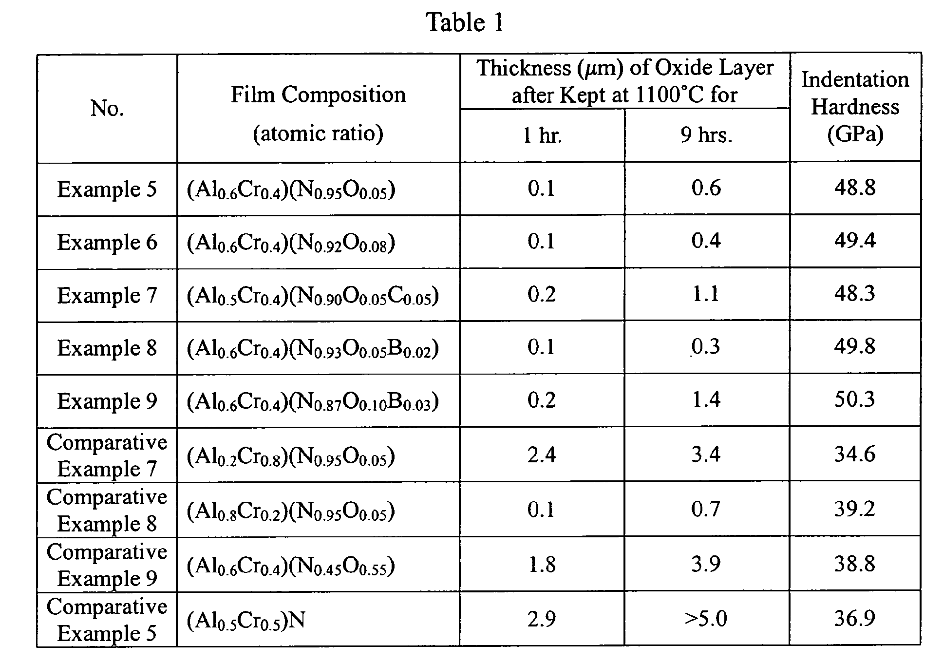
- Hard films having compositions shown in Table 1 were formed on substrates of cemented carbide, high-speed steel and die steel in the same manner as in Example 1.
- Table 1 also shows the oxide layer thickness, indentation hardness, residual compression stress and elastic recovery ratio of each hard film.
- the thickness of the oxide layer was measured after keeping each hard film at 1100°C for 1 hour and 9 hours, respectively, in the air.
- the indentation hardness was measured in the same manner as in Example 2.
- the residual compression stress was calculated from the deformation of a thin plate.
- the elastic recovery ratio was determined by a nano-indentation method.
- each hard film was given a dent at a load of 150 N, to observe the peeling of the film by an optical microscope.
- the results are shown in Table 1.
- the hard films of Examples 5-9 were free from peeling, proving excellent adhesion. This is due to the fact that the hard films of Examples had proper elastic recovery ratios E.
- each hard film of Comparative Examples 5 and 7-9 having a low elastic recovery ratio E failed to follow the deformation of the substrate, resulting in peeling in a portion near the dent.
- Example 10 Using an AlCrSi alloy target having an oxygen content of 3300 ppm produced by a powder metallurgy method to have a targeted composition, and introducing an active gas comprising a nitrogen gas, an oxygen gas and, if necessary, an acetylene gas into a vacuum chamber with the total gas pressure set at 3.0 Pa, a hard film of Example 10 of (Al 0.60 Cr 0.36 Si 0.04 )(N 0.8 C 0.1 O 0.1 ) having a thickness of about 5 ⁇ m was formed on a mirror-polished substrate formed by fine cemented carbide particles containing 13.5% by mass of Co, at a bias voltage of -100 V and at a film-forming temperature of 450°C by an arc-discharge ion-plating method. Also, using the same target as in Example 10 except that its oxygen content was 1800 ppm, a hard film of Comparative Example 10 was formed under the same film-forming conditions as in Example 10.
- X-ray photoelectron spectroscopic analysis was conducted to obtain a wide spectrum for each hard film. And after etching for 30 seconds, X-ray photoelectron spectroscopic analysis was conducted to obtain a narrow spectrum for each hard film.
- X-ray photoelectron spectroscopic analysis was carried out in a circular region having a diameter of 0.4 mm in each hard film at 400 W by an X-ray photoelectron spectroscope of a 1600S type available from PHI using MgK ⁇ as an X-ray source.
- An etching rate by the Ar ion gun was 1.9 nm/minute as converted to SiO 2 .
- the composition of the resultant hard film was determined by an electron probe X-ray microanalysis and an Auger electron spectroscopy.
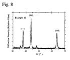
- Fig. 7 indicates the existence of Si and O and the binding energy of Si-O in the hard film of Example 10. It is also clear from an X-ray diffraction pattern shown in Fig. 8 that the hard film of Example 10 has crystal structure oriented most in a (200) face. On the other hand, there was no peak indicating the bonding of oxygen at around 530 eV in the hard film of Comparative Example 10.
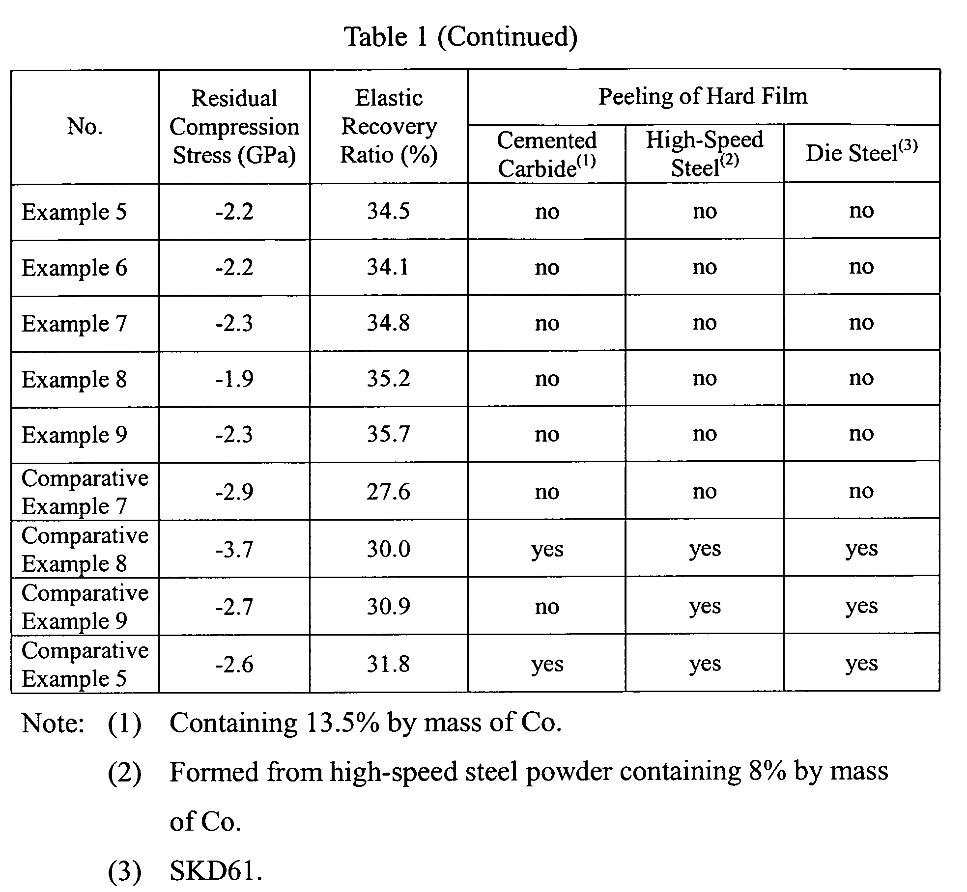
- hard films having compositions shown in Table 2 were formed by an arc-discharge ion-plating method under the film-forming conditions shown in Table 2.
- the intensity of Si-N, Si-O and Si in each hard film was determined by X-ray photoelectron spectroscopy. The results are shown in Table 2.
- Each relative intensity was calculated by peak separation in the Si 2p spectrum of each hard film shown in Table 2, and the peak separation was carried out by a peak-fitting method, with the peak position of Si-N set at 101.2 ⁇ 0.2 eV, the peak position of Si-O set at 103.3 ⁇ 0.2 eV, and the peak position of Si (metal) set at 99.3 ⁇ 0.2 eV.
- Fig. 9 shows a narrow spectrum of Si 2p in Example 12
- Fig. 10 shows a narrow spectrum of Si 2p in Example 16.
- the preferred film-forming conditions for making I(Si-N) / [I(Si-N) + I(Si-O) + I(Si)] of 52% or more are a gas pressure of about 2.0-5.0 Pa, a bias voltage of- 100 V to - 300 V, and a film-forming temperature of 350°C to 500°C.
- I(Si-N) changes not only by the film-forming conditions but also by the film composition.
- Hard films having compositions shown in Table 3 were formed on a mirror-polished substrate of SNMN432 formed by cemented carbide containing 13.5% by mass of Co under the same film-forming conditions as in Example 10. Each hard film was kept at 1100°C for 1 hour and 9 hours, respectively, in the air, to measure the thickness of an oxide layer on each hard film. The results are shown in Table 3 together with those of Comparative Example 5. It is clear from Table 3 that the hard films of Examples 17-21 were not drastically oxidized, proving that they were excellent in a high-temperature oxidation resistance. On the other hand, the hard film of Comparative Example 13 containing 20 atomic % of Al was much more oxidized than those of Examples 17-21, proving that the former was poorer in a high-temperature oxidation resistance.
- the cross section of each of the same hard films was mirror-polished by 0.1- ⁇ m grinding diamond particles with inclination of 5°.
- the indentation hardness of the hard film was measured at a depth of 3.5 ⁇ m from the film surface under the following conditions. Namely, using a micro-indentation hardness tester equipped with a Berkovich-type triangular-pyramidal diamond indenter having a width tip angle of 115°, the indentation hardness of each hard film was measured under the conditions of the maximum load of 49 mN and a loading step of 4.9 mN/sec, with the maximum load kept for 1 second.
- a ratio (T/L) of the thickness T of the hard film to the maximum indentation depth L relative to a load is 10 or more, the hardness of the hard film per se can be measured without influence of the substrate.
- Table 3 shows an average value of 10 measured values.
- Table 3 also shows the residual compression stress of the hard film calculated from the deformation of a thin plate.
- Hard films having compositions shown in Table 3 were formed on ground substrates of SNMN432 formed by cemented carbide containing 13.5% by mass of Co, high-speed steel containing 8% by mass of Co, and SKD die steel, respectively, under the same film-forming conditions as in Example 10.
- An indenter of a Rockwell hardness meter was pressed onto each hard film under a load of 1470 N, to observe by an optical microscope whether or not there was peeling near the dent.
- Table 3 shows the presence and absence of peeling. It is clear from Table 3 that the hard films of Examples 17-21 do not peel from any substrates, exhibiting excellent adhesion. On the other hand, the hard film of Comparative Example 5 could not follow the deformation of the substrate, resulting in peeling in a portion near the dent.
- Coated cutting tools, etc. are microscopically plastically deformed in cutting edges and their vicinities in a cutting stress direction during a cutting operation.
- the cutting edges are plastically deformed, peeling and cracking occur in the hard film, likely to cause irregular wear and damage to the cutting edges.
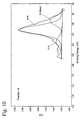
- the plastic deformation resistance of the hard film is important in a kinetic environment accompanied with plastic deformation. Therefore, with respect to the hard films of Examples 17-21 and Comparative Examples 13-15 produced under the same film-forming conditions as in Example 10, load-displacement curves were obtained by the same nano-indentation method as above. The elastic recovery ratio E of each hard film was determined from each load-displacement curve. The results are shown in Table 3 together with those of Comparative Example 5.
- Examples 17-21 had better elastic recovery characteristics than the hard films of Comparative Examples 5 and 13-15. With a high elastic recovery ratio, the peeling and cracking of the hard film are suppressed in a kinetic environment causing wear, etc., proving that the hard film has good adhesion to the substrate. Examples 17-21 reveal that the elastic recovery ratio E is more preferably 30-40%, particularly 32-40%.
- Fig. 11 shows the load-displacement curves of Example 17 and Comparative Example 5. It is clear from Fig. 11 that the hard film of Example 17 is large in the maximum displacement at the maximum load, small in a plastic deformation representing a permanent strain, and large in an elastic recovery ratio when the same stress was applied.
- hard films having compositions shown in Table 3 were formed on the above cemented carbide substrate in the same manner as in Example 10. Each hard film was kept at room temperature, 1100°C and 1200°C, respectively, for 4 hours in vacuum, to measure its micro-indentation hardness in the same manner as above. The results are shown in Table 3.
- the hard films of Examples 17-21 did not suffer from remarkable decrease in hardness in a high-temperature environment.
- the hard film of Comparative Example 5 after kept at 1100°C for 4 hours had indentation hardness of 35.5 GPa, indicating that its hardness decreased to substantially the same level as that of a TiN film.
- C and Co were diffused from the substrate into the hard film after keeping at 1200°C for 4 hours in Comparative Example 5.
- x was 0.2 in Comparative Example 16, 0.3 in Comparative Example 17, 0.5 in Example 22, 0.6 in Example 23, 0.7 in Example 24, and 0.8 in Comparative Example 18.
- x was 0.2 in Comparative Example 19, 0.5 in Comparative Example 20, and 0.7 in Comparative Example 21.
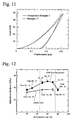
- the indentation hardness of each hard film was measured in the same manner as in Examples 17-21. The results are shown in Fig. 12.
- the hard films of Examples 22-24 having an Al content in a range of 45-75 atomic % had as high hardness as more than 40 GPa because of the inclusion of Si and oxygen.
- the more preferred hardness is 45-55 GPa. With such high hardness, the hard films have excellent wear resistance and adhesion to the substrate.
- a degreased and washed substrate was placed in a vacuum chamber of an arc-discharge ion-plating apparatus, kept at 500°C for 30 minutes and then irradiated with Ar ions for cleaning.
- an N 2 gas and reaction gases selected from a CH 4 gas, a C 2 H 2 gas, an Ar gas, an O 2 gas, a CO gas and a B 3 N 3 H 6 gas depending on the object were introduced into the vacuum chamber, with the total pressure set at 7.5 Pa.
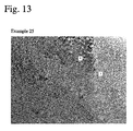
- Fig. 13 is a TEM photograph showing the cross section structure of the hard film of Example 25. In the TEM photograph of Fig. 13, crystal grains 1, 2 and boundaries were clearly observed.
- the oxygen contents in crystal grains and grain boundaries were analyzed by an electron-beam energy-loss spectroscope of Model 766 available from Gatan.
- an analysis region was 1 nm in diameter.
- Fig. 14 shows the analysis results of the crystal grain 2 in Fig. 13 in a region of 1 nm in diameter by the electron-beam energy-loss spectroscopy.
- Fig. 15 shows the analysis results of the boundary (shown by the arrow) in Fig. 13 in a region of 1 nm in diameter by the electron-beam energy-loss spectroscopy.
- Fig. 15 It was confirmed from Fig. 15 that there was oxygen in the grain boundaries. Figs. 14 and 15 indicate that oxygen exists more in grain boundaries than in crystal grains in the hard film. To control such that oxygen exists more in grain boundaries than in crystal grains, the proper film-forming conditions should be selected. In addition, the use of an oxygen-containing metal target is effective.
- X-ray photoelectron spectroscopic analysis was carried out at 400 W in a circular region of 0.4 mm in diameter in the film, using an X-ray photoelectron spectroscope of 1600S type available from PHI, which comprised MgK ⁇ as an X-ray source.
- Each test piece for analysis was sufficiently degreased and washed.
- an Ar ion gun placed with inclination of 50° to a test piece surface
- an X-ray generator was disposed at such a position that X-ray impinges the test piece surface at 90°, and a photoelectron detector was disposed with inclination of 35° relative to the test piece surface.
- a 10-mm 2 -region of each test piece was etched with Ar ions for 120 minutes, and spectrum was measured every 24 minutes.
- a rate of etching with Ar ions was 1.5 nm/min on the basis of SiO 2 .
- Fig. 16 shows the spectrum after etching with Ar ions for 120 minutes. It is clear from Fig. 16 that the hard film of Example 25 contained oxygen.
- Fig. 17 shows the results of element analysis conducted by X-ray photoelectron spectroscopy in a film thickness direction. It was confirmed from Fig. 17 that there was about 6 atomic % of oxygen per the total amount (100 atomic %) of non-metal elements in the hard film of Example 25.
- Fig. 18 shows the spectra corresponding to O 1s measured every 24 minutes. In Fig. 18, the outermost surface of the test piece is shown on a rear end, and the deepest portion of the test piece is shown on a front end. It is clear from Fig.
- Example 25 has the binding energy of metals (Al and Cr) and oxygen in a range of 525-535 eV.
- the bonding was mainly between carbon and oxygen on the test piece surface, while the bonding of metals and oxygen increased as going inside the film.
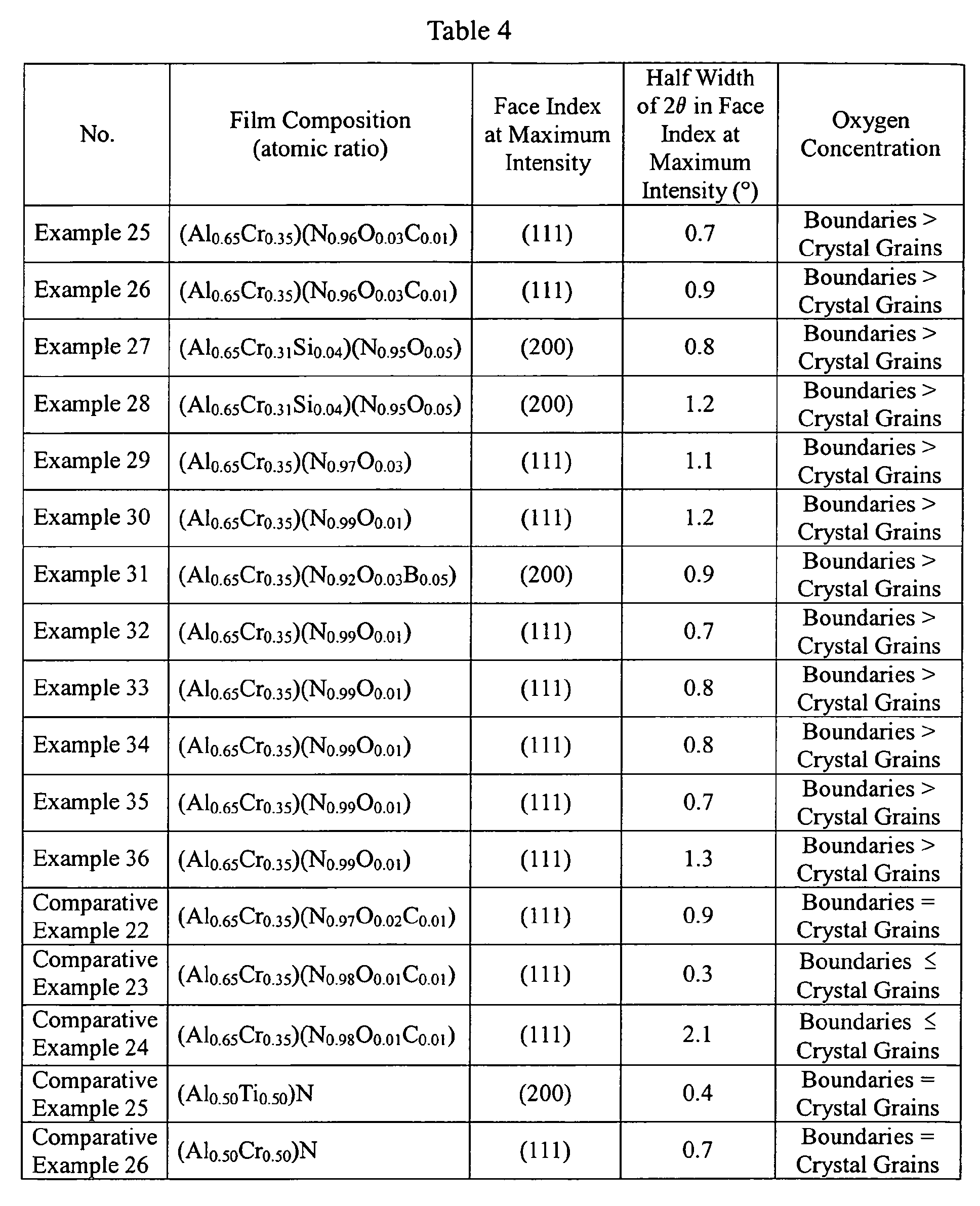
- Table 4 shows the binding energy and bonding state of oxygen to metals in a range of 525-535 eV in each hard film.
- the indentation hardness of each hard film was measured at a depth of 2-3 ⁇ m from the surface at 10 points by the same nano-indentation method as in Examples 17-21.
- the elastic recovery ratio E was calculated from a load-displacement curve obtained by the measurement of the indentation hardness. Table 4 shows an average value of the hardness of each film and the elastic recovery ratio E.
- Each hard film was formed on a four-edge roughing end mill made of high-speed steel having an outer diameter of 12 mm, to measure cutting length until the average wear width of a flank reached 0.25 mm, or when the tool was broken, thereby evaluating the wear resistance of the hard film.
- the results are shown in Table 4.
- the cutting conditions were as follows: Cutting method Rough working on side surface, Work SCM440 (HRC 31), Depth of cutting 6 mm in a radial direction and 12 mm in an axial direction, Cutting speed 70 m/min, Feed 0.07 mm/edge, and Cutting oil None (dry type using air blow).
- the hard films of Examples 25-36 had longer cutting life and better wear resistance than those of Comparative Examples 22-26.
- the hard films ofAlCrSiNO of Examples 27 and 28 had a long cutting life and thus excellent wear resistance.
- the hard film of AlCrNOB of Example 31 had excellent wear resistance because of the inclusion of B.
- Example 32 Rather than Example 32, in which the bonding of oxygen was not clearly observed in a range of 525-535 eV, other Examples, in which the bonding of oxygen was clearly observed, had higher hardness, longer cutting length and better wear resistance.
- Example 33 in which a ratio of I(200) / I(111) was 15, other Examples meeting the conditions of 0.3 ⁇ I(200) / I(111) ⁇ 12 had higher hardness, longer cutting life and better wear resistance.
- Example 34 in which the elastic recovery ratio E determined by a nano-indentation method was 27, other Examples meeting the conditions of 28 ⁇ E ⁇ 42, had higher hardness, higher adhesion, longer cutting length and better wear resistance.
- Example 35 having the peak of the oxygen concentration at a depth within 500 nm from the surface had an excellent high-temperature oxidation resistance and the longest cutting life.
- Example 36 Rather than the hard film of Example 36 having a hexagonal crystal (considered to be AIN) in addition to an NaCl-type crystal structure in X-ray diffraction, the hard films of other Examples having only an NaCl structure had higher hardness, longer cutting life and better wear resistance.
- Comparative Example 22 in which a hard film was formed at a reaction gas pressure of 0.3 Pa, there was no difference in the oxygen concentration observed between crystal grains and grain boundaries, resulting in insufficient hardness and adhesion. Accordingly, the wear resistance was not improved, and the life was short.
- Examples 37-42 each having an additional film shown in Table 5 immediately on the hard film of Example 29 were longer in cutting length and better in wear resistance than the hard film of Example 29.
- Example 43 having an additional film shown in Table 5 immediately on the hard film of Example 31 was longer in cutting life and better in wear resistance than Example 31.
- Examples 44-50 each having an additional film shown in Table 5 immediately on the hard film of Example 27 were longer in cutting length and better in wear resistance than Example 27.
- the tools of Examples 51-53 obtained by smoothing the film surfaces of Examples 45, 46 and 50 by mechanical working had as long life as 1.2 times at maximum.
- the films of TiZrN and VZrN in Comparative Examples 27 and 28 had poor adhesion to the hard film of the present invention, failing to further improve the wear resistance.
- a hard film comprising at least one metal selected from the group consisting of Ti, Cr, Al and Si, and N and at least one non-metal element of C, O and/or B, a hard carbon film, and a boron nitride film immediately on the hard film of the present invention is preferable for increasing the tool life.
- part of the metal components (less than 4 atomic %) may be replaced by one or more metals in 4a, 5a and 6a groups in the hard film.
- the hard film can be provided with improved hardness, adhesion, wear resistance and high-temperature oxidation resistance.
- the cutting life can be extremely improved. With these improvements, the production cost of members requiring the above characteristics is drastically reduced.
Landscapes
- Chemical & Material Sciences (AREA)
- Chemical Kinetics & Catalysis (AREA)
- Engineering & Computer Science (AREA)
- Materials Engineering (AREA)
- Mechanical Engineering (AREA)
- Metallurgy (AREA)
- Organic Chemistry (AREA)
- Physical Vapour Deposition (AREA)
- Cutting Tools, Boring Holders, And Turrets (AREA)
- Polishing Bodies And Polishing Tools (AREA)
- Gloves (AREA)
- Chemical Vapour Deposition (AREA)
Abstract
Description


| Cutting method | Rough working on side surface, |
| Work | SCM440 (HRC 31), |
| Depth of cutting | 6 mm in a radial direction and 12 mm in an axial direction, |
| Cutting speed | 70 m/min, |
| Feed | 0.07 mm/edge, and |
| Cutting oil | None (dry type using air blow). |


| No. | Composition (atomic ratio) | Cutting Length (m) | |
| Hard Film | Additional Film | ||
| Example 37 | (Al0.65Cr0.35)(N0.97O0.03) | (Al0.75Si0.25)(N0.97O0.03) | 72 |
| Example 38 | (Al0.65Cr0.35)(N0.97O0.03) | (Cr0.97Si0.03)(N0.97B0.03) | 75 |
| Example 39 | (Al0.65Cr0.35)(N0.97O0.03) | (Ti0.78Si0.22)N | 89 |
| Example 40 | (Al0.65Cr0.35)(N0.97O0.03) | Hard Carbon | 82 |
| Example 41 | (Al0.65Cr0.35)(N0.97O0.03) | Boron Nitride | 91 |
| Example 42 | (Al0.65Cr0.35)(N0.97O0.03) | Ti(N0.97B0.03) | 93 |
| Example 43 | (Al0.65Cr0.35)(N0.92O0.03B0.05) | Ti(N0.88B0.12) | 95 |
| Example 44 | (Al0.65Cr0.31 Si0.04)(N0.95O0.05) | (Al0.75Si0.25)(N0.97O0.03) | 82 |
| Example 45 | (Al0.65Cr0.31Si0.04)(N0.95O0.05) | (Cr0.97Si0.03)(N0.97B0.03) | 86 |
| Example 46 | (Al0.65Cr0.31 Si0.04)(N0.95O0.05) | (Ti0.78Si0.22)N | 98 |
| Example 47 | (Al0.65Cr0.31 Si0.04)(N0.95O0.05) | Hard Carbon | 102 |
| Example 48 | (Al0.65Cr0.31 Si0.04)(N0.95O0.05) | Boron Nitride | 111 |
| Example 49 | (Al0.65Cr0.31 Si0.04)(N0.95O0.05) | Ti(N0.97B0.03) | 104 |
| Example 50 | (Al0.65Cr0.31Si0.04)(N0.95O0.05) | Ti(N0.88B0.12) | 107 |
| Example 51 | (Al0.65Cr0.31 Si0.04)(N0.95O0.05) | (Cr0.97Si0.03)(N0.97B0.03) | 92 |
| Example 52 | (Al0.65Cr0.31Si0.04)(N0.95O0.05) | (Ti0.78Si0.22)N | 118 |
| Example 53(1) | (Al0.65Cr0.31Si0.04)(N0.95O0.05) | Ti(N0.88B0.12) | 121 |
| Comparative Example 27 | (Al0.65Cr0.35)(N0.97O0.03) (Al0.65Cr0.35)(N0.97O0.03) | (Ti0.78Zr0.22)N (Ti0.78Zr0.22)N | 75 |
| Comparative Example 28 | (Al0.65Cr0.35)(N0.97O0.03) | (V0.75Zr0.25)N | 67 |
Claims (14)
- A hard film formed by an arc-discharge ion-plating method, having a composition comprising metal components represented by AlxCr1-x, wherein x is an atomic ratio meeting 0.45 ≤x ≤0.75, and non-metal components represented by N1-α-β-γBαCβOγ, wherein α, β and γ are respectively atomic ratios meeting 0 ≤α ≤0.15, 0 ≤β ≤0.35, and 0.01 ≤γ ≤0.25; said hard film having the maximum X-ray diffraction intensity in a (200) face or a (111) face, and the binding energy of Al and/or Cr to oxygen in a range of 525-535 eV in an X-ray photoelectron spectroscopy.
- A hard film formed by an arc-discharge ion-plating method, having a composition comprising metal components represented by AlxCr1-x-ySiy, wherein x and y are respectively atomic ratios meeting 0.45 ≤x ≤0.75, and 0<y ≤0.35, and non-metal components represented by N1-α-β-γBαCβOγ, wherein α, β and γ are respectively atomic ratios meeting 0 ≤α ≤0.15, 0 ≤ β ≤0.35, and γ ≤0.25; said hard film having the binding energy of Al, Cr and/or Si to oxygen in a range of 525-535 eV in an X-ray photoelectron spectroscopy.
- The hard film according to claim 2, wherein Si exists in the form of a nitride, an oxide and a metal, and wherein when the relative intensities of the Si metal and its nitride and oxide determined by X-ray photoelectron spectroscopy are represented by I(Si), I(Si-N) and I(Si-O), respectively, with I(Si) + I(Si-N) + I(Si-O) = 100%, I(Si-N) is 52% or more.
- The hard film according to claim 2 or 3, wherein it has a crystal structure having the maximum X-ray diffraction intensity in a (200) face or a (111) face.
- A hard film formed by an arc-discharge ion-plating method, having a composition comprising metal components represented by AlxCr1-x-ySiy, wherein x and y are respectively atomic ratios meeting 0.45 ≤x ≤0.75, 0≤ y ≤0.35, and 0.5 ≤ x + y < 1, and non-metal components represented by N1-α-β-γBαCβOγ, wherein α, β and γ are respectively atomic ratios meeting 0 ≤α ≤0.15, 0 ≤β ≤0.35, and 0.003 ≤γ ≤0.25; said hard film having an NaCl-type crystal structure in an X-ray diffraction, with a half width of 2 at a diffraction peak corresponding to a ( 111 ) face or a (200) face being 0.5-2.0°; and said hard film containing oxygen more in grain boundaries than in crystal grains.
- The hard film according to claim 5, wherein said hard film has the binding energy of Al, Cr and/or Si to oxygen in a range of 525-535 eV in an X-ray photoelectron spectroscopy.
- The hard film according to claim 5 or 6, wherein said hard film has the maximum oxygen concentration in a region of depth within 500 nm from the outermost surface.
- The hard film according to any one of claims 5-7, wherein it meets 0.3 < I(200) / I(111) < 12, wherein I(111) and I(200) are the X-ray diffraction intensities of a (111) face and a (200) face, respectively.
- The hard film according to any one of claims 1-8, wherein its elastic recovery ratio E determined by a nano-indentation method is 28-42%.
- The hard film according to claim 9, wherein said elastic recovery ratio E is 30-40%.
- The hard film according to any one of claims 1-10, wherein it has a surface smoothed by mechanical working.
- The hard film according to any one of claims 1-11, wherein a ratio of said non-metal components to said metal components is 1.1 or more.
- A tool coated with at least one layer of the hard film recited in any one of claims 1-12.
- The hard film-coated tool according to claim 13, wherein another hard film is formed directly on said hard film.
Applications Claiming Priority (6)
| Application Number | Priority Date | Filing Date | Title |
|---|---|---|---|
| JP2002334434A JP3669700B2 (en) | 2002-11-19 | 2002-11-19 | Hard coating |
| JP2002334434 | 2002-11-19 | ||
| JP2002340796 | 2002-11-25 | ||
| JP2002340796A JP3640310B2 (en) | 2002-11-25 | 2002-11-25 | Hard coating |
| JP2003360269 | 2003-10-21 | ||
| JP2003360269A JP2005126736A (en) | 2003-10-21 | 2003-10-21 | Hard film |
Publications (3)
| Publication Number | Publication Date |
|---|---|
| EP1422311A2 true EP1422311A2 (en) | 2004-05-26 |
| EP1422311A3 EP1422311A3 (en) | 2004-08-25 |
| EP1422311B1 EP1422311B1 (en) | 2007-02-28 |
Family
ID=32234002
Family Applications (1)
| Application Number | Title | Priority Date | Filing Date |
|---|---|---|---|
| EP03026508A Expired - Lifetime EP1422311B1 (en) | 2002-11-19 | 2003-11-17 | Hard film and hard film coated tool |
Country Status (8)
| Country | Link |
|---|---|
| US (2) | US7166155B2 (en) |
| EP (1) | EP1422311B1 (en) |
| CN (1) | CN1304626C (en) |
| AT (1) | ATE355395T1 (en) |
| DE (1) | DE60312110T2 (en) |
| DK (1) | DK1422311T3 (en) |
| ES (1) | ES2279050T3 (en) |
| PT (1) | PT1422311E (en) |
Cited By (16)
| Publication number | Priority date | Publication date | Assignee | Title |
|---|---|---|---|---|
| WO2004059030A2 (en) | 2003-04-28 | 2004-07-15 | Unaxis Balzers Ag | Workpiece comprising an alcr-containing hard material layer and production method |
| WO2006102780A1 (en) * | 2005-04-01 | 2006-10-05 | Oerlikon Trading Ag, Trübbach | Multi-layered hard material coating for tools |
| WO2006118513A1 (en) * | 2005-04-29 | 2006-11-09 | Seco Tools Ab | Cutting tool insert, solid end mill or drill coated with wear resistant layer. |
| EP1736565A1 (en) * | 2005-06-22 | 2006-12-27 | Seco Tools Ab | Composite coatings for finishing of hardened steels |
| US7226670B2 (en) | 2003-04-28 | 2007-06-05 | Oc Oerlikon Balzers Ag | Work piece with a hard film of AlCr-containing material, and process for its production |
| WO2007121954A1 (en) * | 2006-04-21 | 2007-11-01 | Cemecon Ag | Coated body |
| EP1710326A4 (en) * | 2003-12-05 | 2008-07-23 | Sumitomo Elec Hardmetal Corp | CUTTING TOOL WITH COATED SURFACE |
| EP1849883A3 (en) * | 2004-09-30 | 2008-08-27 | Kabushiki Kaisha Kobe Seiko Sho | Hard coating excellent in wear resistance and in oxidation resistance and target for forming the same |
| US7537822B2 (en) * | 2005-05-26 | 2009-05-26 | Hitachi Tool Engineering, Ltd. | Hard-coated member |
| US8003231B2 (en) * | 2007-11-15 | 2011-08-23 | Kobe Steel, Ltd. | Wear-resistant member with hard coating |
| EP1842609A4 (en) * | 2005-01-26 | 2012-08-01 | Sumitomo Elec Hardmetal Corp | EDGE REPLACEMENT CUTTING HEAD AND METHOD FOR MANUFACTURING THE SAME |
| WO2013045454A3 (en) * | 2011-09-30 | 2013-05-23 | Cemecon Ag | Coating of substrates using hipims |
| EP1614655B1 (en) | 2004-06-18 | 2015-10-07 | Hitachi Tool Engineering Ltd. | Hard coating and its production method |
| EP3120955A4 (en) * | 2014-03-18 | 2017-10-25 | Hitachi Metals, Ltd. | Coated cutting tool and method for producing same |
| KR102074469B1 (en) | 2019-05-13 | 2020-02-07 | 주식회사 다올플라즈마 | Multilayer Nano Hard Coating Film for Forming Tool |
| DE102022113731A1 (en) | 2022-05-31 | 2023-11-30 | Hartmetall-Werkzeugfabrik Paul Horn Gmbh | Coated tool part and coating process |
Families Citing this family (44)
| Publication number | Priority date | Publication date | Assignee | Title |
|---|---|---|---|---|
| GB2397067B (en) * | 2002-12-23 | 2005-05-11 | Destiny Pharma Ltd | Porphin & azaporphin derivatives with at least one cationic-nitrogen-containing meso-substituent for use in photodynamic therapy & in vitro sterilisation |
| US8668926B1 (en) | 2003-09-15 | 2014-03-11 | Shaker A. Mousa | Nanoparticle and polymer formulations for thyroid hormone analogs, antagonists, and formulations thereof |
| CN1878545A (en) | 2003-09-15 | 2006-12-13 | 奥德威研究院 | Thyroid hormone analogs and methods of use |
| US9198887B2 (en) | 2003-09-15 | 2015-12-01 | Nanopharmaceuticals Llc | Thyroid hormone analogs and methods of use |
| US7785700B2 (en) * | 2004-04-13 | 2010-08-31 | Sumitomo Electric Hardmetal Corp. | Surface-coated cutting tool |
| GB2415372A (en) | 2004-06-23 | 2005-12-28 | Destiny Pharma Ltd | Non photodynamical or sonodynamical antimicrobial use of porphyrins and azaporphyrins containing at least one cationic-nitrogen-containing substituent |
| WO2006070509A1 (en) * | 2004-12-28 | 2006-07-06 | Sumitomo Electric Hardmetal Corp. | Surface-coated cutting tool and process for producing the same |
| JP5143571B2 (en) * | 2005-02-10 | 2013-02-13 | エーリコン・トレイディング・アーゲー・トリューバッハ | High wear resistant triple coating for cutting tools |
| US9498536B2 (en) | 2005-09-15 | 2016-11-22 | Nanopharmaceuticals Llc | Method and composition of thyroid hormone analogues and nanoformulations thereof for treating anti-inflammatory disorders |
| US10130686B2 (en) | 2005-09-15 | 2018-11-20 | Nanopharmaceuticals Llc | Method and composition of thyroid hormone analogues and nanoformulations thereof for treating inflammatory disorders |
| US20100209382A1 (en) | 2005-09-16 | 2010-08-19 | Ordway Research Institute, Inc. | Polyphenol Conjugates as RGD-Binding Compounds and Methods of Use |
| EP2256229A1 (en) * | 2005-11-04 | 2010-12-01 | Sulzer Metaplas GmbH | Layer system to form a surface layer on the surface of a substrate, coating process and substrate with a layer system |
| JP4950499B2 (en) * | 2006-02-03 | 2012-06-13 | 株式会社神戸製鋼所 | Hard coating and method for forming the same |
| JP5096715B2 (en) | 2006-09-21 | 2012-12-12 | 株式会社神戸製鋼所 | Hard coating and hard coating tool |
| EP1918421B1 (en) * | 2006-09-27 | 2017-03-15 | Hitachi Metals, Ltd. | Hard-material-coated member excellent in durability |
| ES2535005T3 (en) | 2006-12-22 | 2015-05-04 | Nanopharmaceuticals Llc | Formulations of nanoparticles and polymers for analogs, antagonists and formulations of thyroid hormone, and uses thereof |
| JP2009039838A (en) * | 2007-08-10 | 2009-02-26 | Mitsubishi Materials Corp | Surface coated cutting tool |
| EP2149620B1 (en) * | 2008-07-31 | 2020-04-29 | Oerlikon Surface Solutions AG, Pfäffikon | Multilayer film-coated member and method for producing it |
| EP2149624B1 (en) * | 2008-07-31 | 2012-08-08 | Sulzer Metaplas GmbH | Multilayer film-coated member and method for producing it |
| CA2736143C (en) * | 2008-10-10 | 2017-04-25 | Oerlikon Trading Ag, Trubbach | Non gamma - phase cubic alcro |
| WO2010120506A1 (en) | 2009-03-31 | 2010-10-21 | Ordway Research Institute, Inc. | Combination treatment of cancer with cetuximab and tetrac |
| WO2010148007A2 (en) | 2009-06-17 | 2010-12-23 | Ordway Research Institute, Inc. | Nanoparticle and polymer formulations for thyroid hormone, analogs, antagonists, and formulations and uses thereof |
| US8557405B2 (en) * | 2009-08-04 | 2013-10-15 | Tungaloy Corporation | Coated member |
| CN102655977B (en) | 2009-12-17 | 2015-01-28 | 住友电气工业株式会社 | Coated rotary tool |
| WO2011095292A1 (en) * | 2010-02-04 | 2011-08-11 | Oerlikon Trading Ag, Trübbach | CUTTING TOOLS WITH Al-Cr-B-N / Ti-Al-N MULTILAYER COATINGS |
| JP5527415B2 (en) * | 2010-08-04 | 2014-06-18 | 株式会社タンガロイ | Coated tool |
| WO2013159870A1 (en) * | 2012-04-22 | 2013-10-31 | Oerlikon Trading Ag, Trübbach | Arc-deposited al-cr-o coatings having enhanced coating properties |
| JP6015423B2 (en) * | 2012-12-21 | 2016-10-26 | 三菱マテリアル株式会社 | Metal nitride material for thermistor, manufacturing method thereof, and film type thermistor sensor |
| JP6015424B2 (en) * | 2012-12-21 | 2016-10-26 | 三菱マテリアル株式会社 | Metal nitride material for thermistor, manufacturing method thereof, and film type thermistor sensor |
| DE102013005437A1 (en) * | 2013-03-29 | 2014-10-02 | Empa | Hard material layers with selected thermal conductivity |
| CN103215542B (en) * | 2013-04-15 | 2015-01-28 | 中国兵器科学研究院宁波分院 | Nanometer multilayer coating and preparation method thereof |
| CN105177498A (en) * | 2015-05-21 | 2015-12-23 | 广东工业大学 | AlCrSiON nano-composite cutting tool coating and preparation method thereof |
| JP6333305B2 (en) * | 2016-04-28 | 2018-05-30 | 大同メタル工業株式会社 | Sliding member |
| EP3463477A4 (en) | 2016-06-07 | 2020-03-04 | NanoPharmaceuticals LLC | NON-CLEAVABLE POLYMER CONJUGED WITH AVSS3 INTEGRINE THYROID HORMONE ANTAGONISTS |
| JP7025727B2 (en) * | 2017-07-18 | 2022-02-25 | 三菱マテリアル株式会社 | Surface cutting tool with excellent chipping resistance and wear resistance with a hard coating layer |
| PL3728695T3 (en) * | 2017-12-22 | 2023-02-06 | Oerlikon Surface Solutions Ag, Pfäffikon | Corrosion- and erosion-resistant coating for turbine blades of gas turbines |
| CN108193181B (en) * | 2018-02-08 | 2019-10-01 | 南京航空航天大学 | The method that TA15 alloy surface reaction magnetocontrol sputtering prepares AlN/AlCrN film |
| US10328043B1 (en) | 2018-04-11 | 2019-06-25 | Nanopharmaceuticals, Llc. | Composition and method for dual targeting in treatment of neuroendocrine tumors |
| US11351137B2 (en) | 2018-04-11 | 2022-06-07 | Nanopharmaceuticals Llc | Composition and method for dual targeting in treatment of neuroendocrine tumors |
| US10961204B1 (en) | 2020-04-29 | 2021-03-30 | Nanopharmaceuticals Llc | Composition of scalable thyrointegrin antagonists with improved blood brain barrier penetration and retention into brain tumors |
| US11723888B2 (en) | 2021-12-09 | 2023-08-15 | Nanopharmaceuticals Llc | Polymer conjugated thyrointegrin antagonists |
| WO2023157466A1 (en) | 2022-02-15 | 2023-08-24 | Seavac株式会社 | Hard coating |
| CN115354275B (en) * | 2022-08-26 | 2023-09-05 | 中国科学院宁波材料技术与工程研究所 | A kind of austenitic stainless steel surface penetration plating compound treatment method and application |
| JP2024054754A (en) * | 2022-10-05 | 2024-04-17 | Tdk株式会社 | Strain resistance film, physical quantity sensor, and method of manufacturing the strain resistance film |
Family Cites Families (14)
| Publication number | Priority date | Publication date | Assignee | Title |
|---|---|---|---|---|
| US2002A (en) * | 1841-03-12 | Tor and planter for plowing | ||
| US6A (en) * | 1836-08-10 | Thomas Blanchard | Machine for forming end pieces of plank blocks for ships | |
| US10A (en) * | 1836-08-10 | Bariah Swift | Dye-wood and dye-stuff cutting and shaving machine | |
| US9A (en) * | 1836-08-10 | Thomas Blanchard | Method of riveting plank or made blocks | |
| US102A (en) * | 1861-08-13 | Whole | ||
| JP3027502B2 (en) | 1993-03-15 | 2000-04-04 | 健 増本 | Abrasion-resistant amorphous hard film and method for producing the same |
| JPH0941127A (en) | 1995-08-03 | 1997-02-10 | Kobe Steel Ltd | Hard film |
| JP3039381B2 (en) * | 1996-07-12 | 2000-05-08 | 山口県 | Method of forming composite hard coating with excellent high temperature oxidation resistance |
| JP3031907B2 (en) * | 1998-03-16 | 2000-04-10 | 日立ツール株式会社 | Multilayer coating member |
| ES2304918T3 (en) * | 2000-03-09 | 2008-11-01 | Sulzer Metaplas Gmbh | PARTS COVERED WITH A HARD COAT. |
| JP3417907B2 (en) * | 2000-07-13 | 2003-06-16 | 日立ツール株式会社 | Multi-layer coating tool |
| JP2002160129A (en) | 2000-11-24 | 2002-06-04 | Toyo Advanced Technologies Co Ltd | Surface treating method of tool |
| ATE545718T1 (en) * | 2000-12-28 | 2012-03-15 | Kobe Steel Ltd | USE OF AN ARC ION PLATING TARGET FOR PRODUCING A HARD FILM |
| DE10233222B4 (en) * | 2001-07-23 | 2007-03-01 | Kabushiki Kaisha Kobe Seiko Sho (Kobe Steel, Ltd.), Kobe | Hard wear-resistant layer, method of forming same and use |
-
2003
- 2003-11-17 ES ES03026508T patent/ES2279050T3/en not_active Expired - Lifetime
- 2003-11-17 EP EP03026508A patent/EP1422311B1/en not_active Expired - Lifetime
- 2003-11-17 DE DE60312110T patent/DE60312110T2/en not_active Expired - Lifetime
- 2003-11-17 PT PT03026508T patent/PT1422311E/en unknown
- 2003-11-17 DK DK03026508T patent/DK1422311T3/en active
- 2003-11-17 AT AT03026508T patent/ATE355395T1/en active
- 2003-11-18 US US10/714,630 patent/US7166155B2/en not_active Expired - Lifetime
- 2003-11-19 CN CNB2003101209355A patent/CN1304626C/en not_active Expired - Lifetime
-
2006
- 2006-11-09 US US11/558,329 patent/US7435487B2/en not_active Expired - Lifetime
Cited By (34)
| Publication number | Priority date | Publication date | Assignee | Title |
|---|---|---|---|---|
| WO2004059030A3 (en) * | 2003-04-28 | 2006-02-02 | Unaxis Balzers Ag | Workpiece comprising an alcr-containing hard material layer and production method |
| US7226670B2 (en) | 2003-04-28 | 2007-06-05 | Oc Oerlikon Balzers Ag | Work piece with a hard film of AlCr-containing material, and process for its production |
| US7988832B2 (en) | 2003-04-28 | 2011-08-02 | Oerlikon Trading Ag, Trubbach | Work piece with a hard film of AlCr-containing material, and process for its production |
| US7851075B2 (en) | 2003-04-28 | 2010-12-14 | Oerlikon Trading Ag, Trubbach | Work piece with a hard film of ALCR-containing material, and process for its production |
| WO2004059030A2 (en) | 2003-04-28 | 2004-07-15 | Unaxis Balzers Ag | Workpiece comprising an alcr-containing hard material layer and production method |
| EP1710326A4 (en) * | 2003-12-05 | 2008-07-23 | Sumitomo Elec Hardmetal Corp | CUTTING TOOL WITH COATED SURFACE |
| EP1614655B2 (en) † | 2004-06-18 | 2018-08-08 | Hitachi Tool Engineering Ltd. | Hard coating and its production method |
| EP1614655B1 (en) | 2004-06-18 | 2015-10-07 | Hitachi Tool Engineering Ltd. | Hard coating and its production method |
| US7601440B2 (en) | 2004-09-30 | 2009-10-13 | Kabushiki Kaisha Kobe Seiko Sho (Kobe Steel, Ltd.) | Hard coating excellent in wear resistance and in oxidation resistance and target for forming the same |
| EP1849883A3 (en) * | 2004-09-30 | 2008-08-27 | Kabushiki Kaisha Kobe Seiko Sho | Hard coating excellent in wear resistance and in oxidation resistance and target for forming the same |
| US7521131B2 (en) | 2004-09-30 | 2009-04-21 | Kobe Steel, Ltd. | Hard coating excellent in wear resistance and in oxidation resistance and target for forming the same |
| EP1842609A4 (en) * | 2005-01-26 | 2012-08-01 | Sumitomo Elec Hardmetal Corp | EDGE REPLACEMENT CUTTING HEAD AND METHOD FOR MANUFACTURING THE SAME |
| US7718043B2 (en) | 2005-04-01 | 2010-05-18 | Oelikon Trading Ag | Multilayer hard coating for tools |
| WO2006102780A1 (en) * | 2005-04-01 | 2006-10-05 | Oerlikon Trading Ag, Trübbach | Multi-layered hard material coating for tools |
| USRE42491E1 (en) | 2005-04-01 | 2011-06-28 | Oerlikon Trading Ag, Trubbach | Multilayer hard coating for tools |
| US7618720B2 (en) | 2005-04-01 | 2009-11-17 | Oerlikon Trading Ag, Trubbach | Multilayer hard coating for tools |
| US7348074B2 (en) | 2005-04-01 | 2008-03-25 | Oc Oerlikon Balzers Ag | Multilayer hard coating for tools |
| CN101151397B (en) * | 2005-04-01 | 2010-12-01 | 奥尔利康贸易股份公司(特吕巴赫) | Multi-layer hard material coating for tools |
| US7592076B2 (en) | 2005-04-29 | 2009-09-22 | Seco Tools Ab | Thin wear resistant layer |
| WO2006118513A1 (en) * | 2005-04-29 | 2006-11-09 | Seco Tools Ab | Cutting tool insert, solid end mill or drill coated with wear resistant layer. |
| US7537822B2 (en) * | 2005-05-26 | 2009-05-26 | Hitachi Tool Engineering, Ltd. | Hard-coated member |
| CN100418679C (en) * | 2005-06-22 | 2008-09-17 | 山高刀具公司 | Composite coatings for finishing of hardened steels |
| EP1736565A1 (en) * | 2005-06-22 | 2006-12-27 | Seco Tools Ab | Composite coatings for finishing of hardened steels |
| WO2007121954A1 (en) * | 2006-04-21 | 2007-11-01 | Cemecon Ag | Coated body |
| US8173278B2 (en) | 2006-04-21 | 2012-05-08 | Cemecon Ag | Coated body |
| US8003231B2 (en) * | 2007-11-15 | 2011-08-23 | Kobe Steel, Ltd. | Wear-resistant member with hard coating |
| US9416440B2 (en) | 2011-09-30 | 2016-08-16 | Cemecon Ag | Coating of substrates using HIPIMS |
| WO2013045454A3 (en) * | 2011-09-30 | 2013-05-23 | Cemecon Ag | Coating of substrates using hipims |
| EP3120955A4 (en) * | 2014-03-18 | 2017-10-25 | Hitachi Metals, Ltd. | Coated cutting tool and method for producing same |
| US10156010B2 (en) | 2014-03-18 | 2018-12-18 | Hitachi Metals, Ltd. | Coated cutting tool and method for producing the same |
| EP3722031A1 (en) * | 2014-03-18 | 2020-10-14 | Hitachi Metals, Ltd. | Coated cutting tool and method for producing the same |
| KR102074469B1 (en) | 2019-05-13 | 2020-02-07 | 주식회사 다올플라즈마 | Multilayer Nano Hard Coating Film for Forming Tool |
| DE102022113731A1 (en) | 2022-05-31 | 2023-11-30 | Hartmetall-Werkzeugfabrik Paul Horn Gmbh | Coated tool part and coating process |
| WO2023232421A1 (en) | 2022-05-31 | 2023-12-07 | Hartmetall-Werkzeugfabrik Paul Horn Gmbh | Coated tool part and coating method |
Also Published As
| Publication number | Publication date |
|---|---|
| US7435487B2 (en) | 2008-10-14 |
| US7166155B2 (en) | 2007-01-23 |
| CN1504589A (en) | 2004-06-16 |
| EP1422311B1 (en) | 2007-02-28 |
| EP1422311A3 (en) | 2004-08-25 |
| CN1304626C (en) | 2007-03-14 |
| US20040137281A1 (en) | 2004-07-15 |
| PT1422311E (en) | 2007-03-30 |
| DK1422311T3 (en) | 2007-06-11 |
| DE60312110D1 (en) | 2007-04-12 |
| US20070087224A1 (en) | 2007-04-19 |
| DE60312110T2 (en) | 2007-10-11 |
| ATE355395T1 (en) | 2006-03-15 |
| ES2279050T3 (en) | 2007-08-16 |
Similar Documents
| Publication | Publication Date | Title |
|---|---|---|
| EP1422311B1 (en) | Hard film and hard film coated tool | |
| EP2208560B1 (en) | Member covered with hard coating film and process for the production of the member | |
| US5656383A (en) | Coated member having excellent hardness and, adhesive properties | |
| EP1710326B1 (en) | Surface-coated cutting tool | |
| EP1736565A1 (en) | Composite coatings for finishing of hardened steels | |
| JP2004238736A (en) | Hard film, and hard film-coated tool | |
| EP1536041A2 (en) | Coated cermet cutting tool with a chipping resistant, hard coating layer | |
| JP3392115B2 (en) | Hard coating tool | |
| Yuan et al. | Relationship of microstructure, mechanical properties and hardened steel cutting performance of TiSiN-based nanocomposite coated tool | |
| EP1135539A1 (en) | Diamond coated cutting tools and method of manufacture | |
| JPH06220571A (en) | Sintered hard alloy and coated sintered hard alloy for cutting tool | |
| JP2008013852A (en) | Hard film, and hard film-coated tool | |
| CN113453828A (en) | Hard film cutting tool | |
| KR20230102643A (en) | Cutting tools with hard coating | |
| JP5098657B2 (en) | Hard coating coated member | |
| JP3404012B2 (en) | Hard coating tool | |
| JP2005126736A (en) | Hard film | |
| KR20130028080A (en) | Cutting tool | |
| JP5023654B2 (en) | Surface-coated cermet cutting tool with excellent crystal grain interface strength, modified α-type Al2O3 layer of hard coating layer | |
| JP4575009B2 (en) | Coated cutting tool | |
| JP3445899B2 (en) | Surface coated end mill | |
| JPH08209334A (en) | Coated hard alloy | |
| JP7132548B2 (en) | surface coated cutting tools | |
| JP2022147327A (en) | Surface coating cutting tool | |
| JP2007291471A (en) | Oxidation-resistant coating film, and member coated by the coating film |
Legal Events
| Date | Code | Title | Description |
|---|---|---|---|
| PUAI | Public reference made under article 153(3) epc to a published international application that has entered the european phase |
Free format text: ORIGINAL CODE: 0009012 |
|
| AK | Designated contracting states |
Kind code of ref document: A2 Designated state(s): AT BE BG CH CY CZ DE DK EE ES FI FR GB GR HU IE IT LI LU MC NL PT RO SE SI SK TR |
|
| AX | Request for extension of the european patent |
Extension state: AL LT LV MK |
|
| PUAL | Search report despatched |
Free format text: ORIGINAL CODE: 0009013 |
|
| AK | Designated contracting states |
Kind code of ref document: A3 Designated state(s): AT BE BG CH CY CZ DE DK EE ES FI FR GB GR HU IE IT LI LU MC NL PT RO SE SI SK TR |
|
| AX | Request for extension of the european patent |
Extension state: AL LT LV MK |
|
| 17P | Request for examination filed |
Effective date: 20041013 |
|
| 17Q | First examination report despatched |
Effective date: 20041115 |
|
| AKX | Designation fees paid |
Designated state(s): AT BE BG CH CY CZ DE DK EE ES FI FR GB GR HU IE IT LI LU MC NL PT RO SE SI SK TR |
|
| GRAP | Despatch of communication of intention to grant a patent |
Free format text: ORIGINAL CODE: EPIDOSNIGR1 |
|
| GRAS | Grant fee paid |
Free format text: ORIGINAL CODE: EPIDOSNIGR3 |
|
| GRAA | (expected) grant |
Free format text: ORIGINAL CODE: 0009210 |
|
| AK | Designated contracting states |
Kind code of ref document: B1 Designated state(s): AT BE BG CH CY CZ DE DK EE ES FI FR GB GR HU IE IT LI LU MC NL PT RO SE SI SK TR |
|
| PG25 | Lapsed in a contracting state [announced via postgrant information from national office to epo] |
Ref country code: SI Free format text: LAPSE BECAUSE OF FAILURE TO SUBMIT A TRANSLATION OF THE DESCRIPTION OR TO PAY THE FEE WITHIN THE PRESCRIBED TIME-LIMIT Effective date: 20070228 |
|
| REG | Reference to a national code |
Ref country code: GB Ref legal event code: FG4D |
|
| REG | Reference to a national code |
Ref country code: CH Ref legal event code: NV Representative=s name: TROESCH SCHEIDEGGER WERNER AG Ref country code: PT Ref legal event code: SC4A Free format text: AVAILABILITY OF NATIONAL TRANSLATION Effective date: 20070302 Ref country code: CH Ref legal event code: EP |
|
| REF | Corresponds to: |
Ref document number: 60312110 Country of ref document: DE Date of ref document: 20070412 Kind code of ref document: P |
|
| REG | Reference to a national code |
Ref country code: IE Ref legal event code: FG4D |
|
| REG | Reference to a national code |
Ref country code: GR Ref legal event code: EP Ref document number: 20070400688 Country of ref document: GR |
|
| REG | Reference to a national code |
Ref country code: HU Ref legal event code: AG4A Ref document number: E001308 Country of ref document: HU |
|
| PG25 | Lapsed in a contracting state [announced via postgrant information from national office to epo] |
Ref country code: BG Free format text: LAPSE BECAUSE OF EXPIRATION OF PROTECTION Effective date: 20070529 |
|
| REG | Reference to a national code |
Ref country code: SE Ref legal event code: TRGR |
|
| REG | Reference to a national code |
Ref country code: ES Ref legal event code: FG2A Ref document number: 2279050 Country of ref document: ES Kind code of ref document: T3 |
|
| ET | Fr: translation filed | ||
| PG25 | Lapsed in a contracting state [announced via postgrant information from national office to epo] |
Ref country code: SK Free format text: LAPSE BECAUSE OF FAILURE TO SUBMIT A TRANSLATION OF THE DESCRIPTION OR TO PAY THE FEE WITHIN THE PRESCRIBED TIME-LIMIT Effective date: 20070228 |
|
| PLBI | Opposition filed |
Free format text: ORIGINAL CODE: 0009260 |
|
| PG25 | Lapsed in a contracting state [announced via postgrant information from national office to epo] |
Ref country code: RO Free format text: LAPSE BECAUSE OF FAILURE TO SUBMIT A TRANSLATION OF THE DESCRIPTION OR TO PAY THE FEE WITHIN THE PRESCRIBED TIME-LIMIT Effective date: 20070228 |
|
| 26 | Opposition filed |
Opponent name: SANDVIK INTELLECTUAL PROPERTY Effective date: 20071128 |
|
| PLAX | Notice of opposition and request to file observation + time limit sent |
Free format text: ORIGINAL CODE: EPIDOSNOBS2 |
|
| NLR1 | Nl: opposition has been filed with the epo |
Opponent name: SANDVIK INTELLECTUAL PROPERTY |
|
| PLAF | Information modified related to communication of a notice of opposition and request to file observations + time limit |
Free format text: ORIGINAL CODE: EPIDOSCOBS2 |
|
| PG25 | Lapsed in a contracting state [announced via postgrant information from national office to epo] |
Ref country code: MC Free format text: LAPSE BECAUSE OF NON-PAYMENT OF DUE FEES Effective date: 20071130 |
|
| PLBB | Reply of patent proprietor to notice(s) of opposition received |
Free format text: ORIGINAL CODE: EPIDOSNOBS3 |
|
| PG25 | Lapsed in a contracting state [announced via postgrant information from national office to epo] |
Ref country code: EE Free format text: LAPSE BECAUSE OF FAILURE TO SUBMIT A TRANSLATION OF THE DESCRIPTION OR TO PAY THE FEE WITHIN THE PRESCRIBED TIME-LIMIT Effective date: 20070228 |
|
| PLBD | Termination of opposition procedure: decision despatched |
Free format text: ORIGINAL CODE: EPIDOSNOPC1 |
|
| PLBP | Opposition withdrawn |
Free format text: ORIGINAL CODE: 0009264 |
|
| PG25 | Lapsed in a contracting state [announced via postgrant information from national office to epo] |
Ref country code: CY Free format text: LAPSE BECAUSE OF FAILURE TO SUBMIT A TRANSLATION OF THE DESCRIPTION OR TO PAY THE FEE WITHIN THE PRESCRIBED TIME-LIMIT Effective date: 20070228 |
|
| PG25 | Lapsed in a contracting state [announced via postgrant information from national office to epo] |
Ref country code: LU Free format text: LAPSE BECAUSE OF NON-PAYMENT OF DUE FEES Effective date: 20071117 |
|
| PLBM | Termination of opposition procedure: date of legal effect published |
Free format text: ORIGINAL CODE: 0009276 |
|
| STAA | Information on the status of an ep patent application or granted ep patent |
Free format text: STATUS: OPPOSITION PROCEDURE CLOSED |
|
| 27C | Opposition proceedings terminated |
Effective date: 20090619 |
|
| NLR2 | Nl: decision of opposition |
Effective date: 20090619 |
|
| REG | Reference to a national code |
Ref country code: NL Ref legal event code: TD Effective date: 20150806 |
|
| REG | Reference to a national code |
Ref country code: CH Ref legal event code: PFA Owner name: MITSUBISHI HITACHI TOOL ENGINEERING, LTD., JP Free format text: FORMER OWNER: HITACHI TOOL ENGINEERING LTD., JP |
|
| REG | Reference to a national code |
Ref country code: DE Ref legal event code: R082 Ref document number: 60312110 Country of ref document: DE Representative=s name: PATENTANWAELTE STREHL, SCHUEBEL-HOPF & PARTNER, DE Ref country code: DE Ref legal event code: R081 Ref document number: 60312110 Country of ref document: DE Owner name: MITSUBISHI HITACHI TOOL ENGINEERING, LTD., JP Free format text: FORMER OWNER: HITACHI TOOL ENGINEERING LTD., TOKIO/TOKYO, JP Ref country code: DE Ref legal event code: R082 Ref document number: 60312110 Country of ref document: DE Representative=s name: STREHL SCHUEBEL-HOPF & PARTNER MBB PATENTANWAE, DE |
|
| REG | Reference to a national code |
Ref country code: HU Ref legal event code: HC9C Owner name: MITSUBISHI HITACHI TOOL ENGINEERING, LTD., JP Free format text: FORMER OWNER(S): HITACHI TOOL ENGINEERING LTD., JP |
|
| REG | Reference to a national code |
Ref country code: FR Ref legal event code: PLFP Year of fee payment: 13 |
|
| REG | Reference to a national code |
Ref country code: FR Ref legal event code: CD Owner name: MITSUBISHI HITACHI TOOL ENGINEERING, LTD. Effective date: 20151123 |
|
| PGFP | Annual fee paid to national office [announced via postgrant information from national office to epo] |
Ref country code: GR Payment date: 20151015 Year of fee payment: 13 Ref country code: FI Payment date: 20151111 Year of fee payment: 13 Ref country code: DK Payment date: 20151110 Year of fee payment: 13 Ref country code: IE Payment date: 20151109 Year of fee payment: 13 Ref country code: TR Payment date: 20151021 Year of fee payment: 13 |
|
| PGFP | Annual fee paid to national office [announced via postgrant information from national office to epo] |
Ref country code: NL Payment date: 20151012 Year of fee payment: 13 Ref country code: BE Payment date: 20151111 Year of fee payment: 13 Ref country code: HU Payment date: 20151014 Year of fee payment: 13 |
|
| REG | Reference to a national code |
Ref country code: FR Ref legal event code: PLFP Year of fee payment: 14 |
|
| PG25 | Lapsed in a contracting state [announced via postgrant information from national office to epo] |
Ref country code: BE Free format text: LAPSE BECAUSE OF NON-PAYMENT OF DUE FEES Effective date: 20161130 |
|
| REG | Reference to a national code |
Ref country code: AT Ref legal event code: HC Ref document number: 355395 Country of ref document: AT Kind code of ref document: T Owner name: MITSUBISHI HITACHI TOOL ENGINEERING, LTD., JP Effective date: 20170119 |
|
| REG | Reference to a national code |
Ref country code: DK Ref legal event code: EBP Effective date: 20161130 |
|
| REG | Reference to a national code |
Ref country code: NL Ref legal event code: MM Effective date: 20161201 |
|
| PG25 | Lapsed in a contracting state [announced via postgrant information from national office to epo] |
Ref country code: FI Free format text: LAPSE BECAUSE OF NON-PAYMENT OF DUE FEES Effective date: 20161117 Ref country code: GR Free format text: LAPSE BECAUSE OF NON-PAYMENT OF DUE FEES Effective date: 20170612 |
|
| REG | Reference to a national code |
Ref country code: IE Ref legal event code: MM4A |
|
| PG25 | Lapsed in a contracting state [announced via postgrant information from national office to epo] |
Ref country code: HU Free format text: LAPSE BECAUSE OF NON-PAYMENT OF DUE FEES Effective date: 20161118 |
|
| PG25 | Lapsed in a contracting state [announced via postgrant information from national office to epo] |
Ref country code: NL Free format text: LAPSE BECAUSE OF NON-PAYMENT OF DUE FEES Effective date: 20161201 |
|
| REG | Reference to a national code |
Ref country code: FR Ref legal event code: PLFP Year of fee payment: 15 |
|
| PG25 | Lapsed in a contracting state [announced via postgrant information from national office to epo] |
Ref country code: DK Free format text: LAPSE BECAUSE OF NON-PAYMENT OF DUE FEES Effective date: 20161130 Ref country code: IE Free format text: LAPSE BECAUSE OF NON-PAYMENT OF DUE FEES Effective date: 20161117 |
|
| REG | Reference to a national code |
Ref country code: BE Ref legal event code: HC Owner name: MITSHUBISHI HITACHI TOOL ENGINEERING, LTD.; JP Free format text: DETAILS ASSIGNMENT: CHANGE OF OWNER(S), CHANGEMENT NOM PROPRIETAIRE, NOM + ADRESSE; FORMER OWNER NAME: HITACHI TOOL ENGINEERING LTD. Effective date: 20151007 Ref country code: BE Ref legal event code: HC Owner name: MITSUBISHI HITACHI TOOL ENGINEERING, LTD.; JP Free format text: DETAILS ASSIGNMENT: CHANGE OF OWNER(S), CHANGEMENT NOM PROPRIETAIRE, CORRECTION DU NOM; FORMER OWNER NAME: MITSHUBISHI HITACHI TOOL ENGINEERING, LTD. Effective date: 20151104 Ref country code: BE Ref legal event code: MM Effective date: 20161130 |
|
| REG | Reference to a national code |
Ref country code: FR Ref legal event code: PLFP Year of fee payment: 16 |
|
| PG25 | Lapsed in a contracting state [announced via postgrant information from national office to epo] |
Ref country code: TR Free format text: LAPSE BECAUSE OF NON-PAYMENT OF DUE FEES Effective date: 20161117 |
|
| PGFP | Annual fee paid to national office [announced via postgrant information from national office to epo] |
Ref country code: GB Payment date: 20220930 Year of fee payment: 20 |
|
| PGFP | Annual fee paid to national office [announced via postgrant information from national office to epo] |
Ref country code: FR Payment date: 20221010 Year of fee payment: 20 |
|
| PGFP | Annual fee paid to national office [announced via postgrant information from national office to epo] |
Ref country code: SE Payment date: 20221011 Year of fee payment: 20 Ref country code: PT Payment date: 20221116 Year of fee payment: 20 Ref country code: IT Payment date: 20221011 Year of fee payment: 20 Ref country code: ES Payment date: 20221206 Year of fee payment: 20 Ref country code: DE Payment date: 20220930 Year of fee payment: 20 Ref country code: CZ Payment date: 20221027 Year of fee payment: 20 Ref country code: AT Payment date: 20221025 Year of fee payment: 20 |
|
| PGFP | Annual fee paid to national office [announced via postgrant information from national office to epo] |
Ref country code: CH Payment date: 20221103 Year of fee payment: 20 |
|
| REG | Reference to a national code |
Ref country code: DE Ref legal event code: R071 Ref document number: 60312110 Country of ref document: DE |
|
| REG | Reference to a national code |
Ref country code: ES Ref legal event code: FD2A Effective date: 20231124 |
|
| REG | Reference to a national code |
Ref country code: CH Ref legal event code: PL |
|
| REG | Reference to a national code |
Ref country code: GB Ref legal event code: PE20 Expiry date: 20231116 |
|
| REG | Reference to a national code |
Ref country code: SE Ref legal event code: EUG |
|
| REG | Reference to a national code |
Ref country code: AT Ref legal event code: MK07 Ref document number: 355395 Country of ref document: AT Kind code of ref document: T Effective date: 20231117 |
|
| PG25 | Lapsed in a contracting state [announced via postgrant information from national office to epo] |
Ref country code: GB Free format text: LAPSE BECAUSE OF EXPIRATION OF PROTECTION Effective date: 20231116 |
|
| PG25 | Lapsed in a contracting state [announced via postgrant information from national office to epo] |
Ref country code: ES Free format text: LAPSE BECAUSE OF EXPIRATION OF PROTECTION Effective date: 20231118 |
|
| PG25 | Lapsed in a contracting state [announced via postgrant information from national office to epo] |
Ref country code: PT Free format text: LAPSE BECAUSE OF EXPIRATION OF PROTECTION Effective date: 20231127 Ref country code: GB Free format text: LAPSE BECAUSE OF EXPIRATION OF PROTECTION Effective date: 20231116 Ref country code: ES Free format text: LAPSE BECAUSE OF EXPIRATION OF PROTECTION Effective date: 20231118 Ref country code: CZ Free format text: LAPSE BECAUSE OF EXPIRATION OF PROTECTION Effective date: 20231117 |