EP1422055A1 - Capacitor layer forming both-side copper-clad laminated heet and production method therefor - Google Patents
Capacitor layer forming both-side copper-clad laminated heet and production method therefor Download PDFInfo
- Publication number
- EP1422055A1 EP1422055A1 EP02751721A EP02751721A EP1422055A1 EP 1422055 A1 EP1422055 A1 EP 1422055A1 EP 02751721 A EP02751721 A EP 02751721A EP 02751721 A EP02751721 A EP 02751721A EP 1422055 A1 EP1422055 A1 EP 1422055A1
- Authority
- EP
- European Patent Office
- Prior art keywords
- layer
- heat resistant
- resistant film
- clad laminate
- thermosetting resin
- Prior art date
- Legal status (The legal status is an assumption and is not a legal conclusion. Google has not performed a legal analysis and makes no representation as to the accuracy of the status listed.)
- Granted
Links
Images


Classifications
-
- H—ELECTRICITY
- H05—ELECTRIC TECHNIQUES NOT OTHERWISE PROVIDED FOR
- H05K—PRINTED CIRCUITS; CASINGS OR CONSTRUCTIONAL DETAILS OF ELECTRIC APPARATUS; MANUFACTURE OF ASSEMBLAGES OF ELECTRICAL COMPONENTS
- H05K1/00—Printed circuits
- H05K1/18—Printed circuits structurally associated with non-printed electric components
-
- H—ELECTRICITY
- H05—ELECTRIC TECHNIQUES NOT OTHERWISE PROVIDED FOR
- H05K—PRINTED CIRCUITS; CASINGS OR CONSTRUCTIONAL DETAILS OF ELECTRIC APPARATUS; MANUFACTURE OF ASSEMBLAGES OF ELECTRICAL COMPONENTS
- H05K1/00—Printed circuits
- H05K1/16—Printed circuits incorporating printed electric components, e.g. printed resistors, capacitors or inductors
- H05K1/162—Printed circuits incorporating printed electric components, e.g. printed resistors, capacitors or inductors incorporating printed capacitors
-
- B—PERFORMING OPERATIONS; TRANSPORTING
- B32—LAYERED PRODUCTS
- B32B—LAYERED PRODUCTS, i.e. PRODUCTS BUILT-UP OF STRATA OF FLAT OR NON-FLAT, e.g. CELLULAR OR HONEYCOMB, FORM
- B32B15/00—Layered products comprising a layer of metal
- B32B15/04—Layered products comprising a layer of metal comprising metal as the main or only constituent of a layer, which is next to another layer of the same or of a different material
- B32B15/08—Layered products comprising a layer of metal comprising metal as the main or only constituent of a layer, which is next to another layer of the same or of a different material of synthetic resin
-
- H—ELECTRICITY
- H01—ELECTRIC ELEMENTS
- H01G—CAPACITORS; CAPACITORS, RECTIFIERS, DETECTORS, SWITCHING DEVICES, LIGHT-SENSITIVE OR TEMPERATURE-SENSITIVE DEVICES OF THE ELECTROLYTIC TYPE
- H01G4/00—Fixed capacitors; Processes of their manufacture
- H01G4/002—Details
- H01G4/018—Dielectrics
- H01G4/06—Solid dielectrics
- H01G4/14—Organic dielectrics
- H01G4/18—Organic dielectrics of synthetic material, e.g. derivatives of cellulose
-
- H—ELECTRICITY
- H10—SEMICONDUCTOR DEVICES; ELECTRIC SOLID-STATE DEVICES NOT OTHERWISE PROVIDED FOR
- H10D—INORGANIC ELECTRIC SEMICONDUCTOR DEVICES
- H10D62/00—Semiconductor bodies, or regions thereof, of devices having potential barriers
- H10D62/10—Shapes, relative sizes or dispositions of the regions of the semiconductor bodies; Shapes of the semiconductor bodies
-
- B—PERFORMING OPERATIONS; TRANSPORTING
- B32—LAYERED PRODUCTS
- B32B—LAYERED PRODUCTS, i.e. PRODUCTS BUILT-UP OF STRATA OF FLAT OR NON-FLAT, e.g. CELLULAR OR HONEYCOMB, FORM
- B32B2305/00—Condition, form or state of the layers or laminate
- B32B2305/74—Partially cured
-
- B—PERFORMING OPERATIONS; TRANSPORTING
- B32—LAYERED PRODUCTS
- B32B—LAYERED PRODUCTS, i.e. PRODUCTS BUILT-UP OF STRATA OF FLAT OR NON-FLAT, e.g. CELLULAR OR HONEYCOMB, FORM
- B32B2311/00—Metals, their alloys or their compounds
- B32B2311/12—Copper
-
- B—PERFORMING OPERATIONS; TRANSPORTING
- B32—LAYERED PRODUCTS
- B32B—LAYERED PRODUCTS, i.e. PRODUCTS BUILT-UP OF STRATA OF FLAT OR NON-FLAT, e.g. CELLULAR OR HONEYCOMB, FORM
- B32B2398/00—Unspecified macromolecular compounds
- B32B2398/10—Thermosetting resins
-
- B—PERFORMING OPERATIONS; TRANSPORTING
- B32—LAYERED PRODUCTS
- B32B—LAYERED PRODUCTS, i.e. PRODUCTS BUILT-UP OF STRATA OF FLAT OR NON-FLAT, e.g. CELLULAR OR HONEYCOMB, FORM
- B32B2457/00—Electrical equipment
- B32B2457/16—Capacitors
-
- H—ELECTRICITY
- H05—ELECTRIC TECHNIQUES NOT OTHERWISE PROVIDED FOR
- H05K—PRINTED CIRCUITS; CASINGS OR CONSTRUCTIONAL DETAILS OF ELECTRIC APPARATUS; MANUFACTURE OF ASSEMBLAGES OF ELECTRICAL COMPONENTS
- H05K2201/00—Indexing scheme relating to printed circuits covered by H05K1/00
- H05K2201/01—Dielectrics
- H05K2201/0104—Properties and characteristics in general
- H05K2201/0129—Thermoplastic polymer, e.g. auto-adhesive layer; Shaping of thermoplastic polymer
-
- H—ELECTRICITY
- H05—ELECTRIC TECHNIQUES NOT OTHERWISE PROVIDED FOR
- H05K—PRINTED CIRCUITS; CASINGS OR CONSTRUCTIONAL DETAILS OF ELECTRIC APPARATUS; MANUFACTURE OF ASSEMBLAGES OF ELECTRICAL COMPONENTS
- H05K2201/00—Indexing scheme relating to printed circuits covered by H05K1/00
- H05K2201/01—Dielectrics
- H05K2201/0183—Dielectric layers
- H05K2201/0195—Dielectric or adhesive layers comprising a plurality of layers, e.g. in a multilayer structure
-
- H—ELECTRICITY
- H05—ELECTRIC TECHNIQUES NOT OTHERWISE PROVIDED FOR
- H05K—PRINTED CIRCUITS; CASINGS OR CONSTRUCTIONAL DETAILS OF ELECTRIC APPARATUS; MANUFACTURE OF ASSEMBLAGES OF ELECTRICAL COMPONENTS
- H05K2201/00—Indexing scheme relating to printed circuits covered by H05K1/00
- H05K2201/02—Fillers; Particles; Fibers; Reinforcement materials
- H05K2201/0203—Fillers and particles
- H05K2201/0206—Materials
- H05K2201/0209—Inorganic, non-metallic particles
-
- H—ELECTRICITY
- H05—ELECTRIC TECHNIQUES NOT OTHERWISE PROVIDED FOR
- H05K—PRINTED CIRCUITS; CASINGS OR CONSTRUCTIONAL DETAILS OF ELECTRIC APPARATUS; MANUFACTURE OF ASSEMBLAGES OF ELECTRICAL COMPONENTS
- H05K2201/00—Indexing scheme relating to printed circuits covered by H05K1/00
- H05K2201/03—Conductive materials
- H05K2201/0332—Structure of the conductor
- H05K2201/0335—Layered conductors or foils
- H05K2201/0355—Metal foils
-
- H—ELECTRICITY
- H05—ELECTRIC TECHNIQUES NOT OTHERWISE PROVIDED FOR
- H05K—PRINTED CIRCUITS; CASINGS OR CONSTRUCTIONAL DETAILS OF ELECTRIC APPARATUS; MANUFACTURE OF ASSEMBLAGES OF ELECTRICAL COMPONENTS
- H05K2201/00—Indexing scheme relating to printed circuits covered by H05K1/00
- H05K2201/09—Shape and layout
- H05K2201/09209—Shape and layout details of conductors
- H05K2201/0929—Conductive planes
- H05K2201/09309—Core having two or more power planes; Capacitive laminate of two power planes
-
- H—ELECTRICITY
- H05—ELECTRIC TECHNIQUES NOT OTHERWISE PROVIDED FOR
- H05K—PRINTED CIRCUITS; CASINGS OR CONSTRUCTIONAL DETAILS OF ELECTRIC APPARATUS; MANUFACTURE OF ASSEMBLAGES OF ELECTRICAL COMPONENTS
- H05K2203/00—Indexing scheme relating to apparatus or processes for manufacturing printed circuits covered by H05K3/00
- H05K2203/03—Metal processing
- H05K2203/0307—Providing micro- or nanometer scale roughness on a metal surface, e.g. by plating of nodules or dendrites
-
- H—ELECTRICITY
- H05—ELECTRIC TECHNIQUES NOT OTHERWISE PROVIDED FOR
- H05K—PRINTED CIRCUITS; CASINGS OR CONSTRUCTIONAL DETAILS OF ELECTRIC APPARATUS; MANUFACTURE OF ASSEMBLAGES OF ELECTRICAL COMPONENTS
- H05K3/00—Apparatus or processes for manufacturing printed circuits
- H05K3/38—Improvement of the adhesion between the insulating substrate and the metal
- H05K3/382—Improvement of the adhesion between the insulating substrate and the metal by special treatment of the metal
- H05K3/384—Improvement of the adhesion between the insulating substrate and the metal by special treatment of the metal by plating
Definitions
- the present invention relates to a double-sided copper clad laminate for forming a capacitor layer in an internal layer of a multilayer printed wiring board and a method for manufacturing the same.
- the server has a bulk memory for enabling concentrated management of a large quantity of information, and is required to have a high operation performance enough to accommodate simultaneous accesses from a plurality of computers. Therefore, the server is required to have a higher signal transfer rate and to be less susceptible to malfunction.
- a circuit design of a printed wiring board for implementing them is very important.
- manufacturers of the printed wiring board have devised various measures. For example, in terms of structure, the multilayer printed wiring board has been developed, or in terms of circuit configuration, the circuit design has been modified to shorten a signal transfer length.
- a capacitor serves to supply operating power for a device with stability, and is typically arranged on an external layer of the printed wiring board.
- the capacitor can be thinned and the thinned capacitor can exhibit good properties, a method of using a double-sided copper clad laminate to provide a capacitor in an internal layer of a multilayer printed wiring board has become common.
- a capacitor layer is formed using the thin double-sided copper clad laminate.
- an FR-4 base material which is a glass cloth impregnated with epoxy resin, is used as an insulating material, and copper foils are applied to both sides of the base material.
- the thinnest possible FR-4 base material has been used.
- the member for forming an embedded capacitor layer which is the double-sided copper clad laminate including the FR-4 base material, has the glass cloth serving as an aggregate in the insulating layer. Therefore, in thickness control of the member, there is a certain lower limit.
- a waviness shape of the glass cloth may appear on the surface of the laminate, so that it is difficult to provide a completely flat surface. For example, when a prepreg including a glass cloth as a frame member is used to form the insulating layer, a limit thickness of the prepreg is 50 ⁇ m.
- an electrodeposited copper foil is generally used as the copper foils constituting the thin double-sided copper clad laminate for forming the capacitor layer.
- the interface of the electrodeposited copper foil with the resin layer is subject to a nodular treatment to have irregularities, which are intended to provide an anchoring effect for enhancing the adhessiveness between the electrodeposited copper foil and the resin layer.
- the nodular-treated surfaces of the copper foils become close to each other. Then, if the nodular-treated surfaces have an abnormally developed part, a short-circuit occurs partially between the copper foils, and when a voltage is applied between the copper foils, a current flows from one copper foil to another, which is a significant problem in thinning the insulating layer.
- the copper clad laminate used as the member for forming the embedded capacitor layer can be readily bent because of its thin insulating layer, so that a fracture readily occurs in the insulating layer. Thus, handling of such a copper clad laminate has been difficult.
- the copper clad laminate contains a filler, there is a problem in that the insulating layer becomes brittle. If the insulating layer is thin and lacks strength, there is a problem in forming the capacitor circuit through etching.
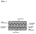
- Fig. 1 is a schematic cross-sectional view of a double-sided copper clad laminate for forming a capacitor layer.
- Figs. 2 and 3 are conceptual diagram illustrating a method for manufacturing the double-sided copper clad laminate for forming a capacitor layer.
- Fig. 4 is a schematic cross-sectional view of a double-sided copper clad laminate for forming a capacitor layer.
- a double-sided copper clad laminate for forming a capacitor layer has a layered structure comprising conductive copper foil layers arranged at outer layers thereof and a resin layer, which is dielectric, sandwiched between the copper foils, and is characterized in that the resin layer has a three-layer structure comprising a thermosetting resin layer, a heat resistant film layer and a thermosetting resin layer in this order and has a total thickness of 25 ⁇ m or less, the thermosetting resin layer is made of epoxy resin material, and the heat resistant film layer is made of a resin material that has ordinary properties of a Young's modulus of 300kg/mm 2 or more, a tensile strength of 20 kg/mm 2 or more and an elongation percentage of 5% or more, a softening point higher than a molding temperature for the thermosetting resin forming the thermosetting resin layers on both sides thereof, and a relative dielectric constant of 2.5 or more.
- the double-sided copper clad laminate for forming a capacitor layer as set forth in a claim is characterized in that it has the three-layer structure comprising the thermosetting resin layer, the heat resistant film layer and the thermosetting resin layer in this order.
- the shown three-layer structure demonstrates that the three-layer structure can be clearly recognized after the double-sided copper clad laminate is provided by hot pressing. Thus, all of the three layers must not be softened to form a mixed layer during the hot pressing in the manufacture thereof.
- the heat resistant film layer must be made of a resin material having a softening point higher than a molding temperature for the thermosetting resin forming the thermosetting resin layers on both sides of the heat resistant film layer.
- the softening point is measured according to Vicat softening point test method defined in JIS K 7206.
- the resin layer having the three-layer structure comprising the thermosetting resin layer, the heat resistant film layer and the thermosetting resin layer in this order must have a total thickness of 25 ⁇ m or less.
- the resin layer constitutes the dielectric layer in the capacitor.
- An electric capacity of a capacitor is inversely proportional to the thickness of the dielectric layer. Accordingly, as the dielectric layer becomes thinner, the electric capacity and the quantity of stored electricity become larger. The stored electricity contributes part of power supply, leading to power saving. Since the thickness of the resin layer is determined in stages of product design or circuit design, it is determined to be 25 ⁇ m or less in consideration of market requirements.
- the heat resistant film layer needs to have ordinary properties of a Young's modulus of 300kg/mm 2 or more, a tensile strength of 20 kg/mm 2 or more and an elongation percentage of 5% or more.
- Such mechanical properties are defined in order to prevent tearing of the resin layer from being caused by showering of an etchant during etching to form a capacitor circuit pattern as described above. That is, when the heat resistant film layer, which is an intermediate layer of the three-layer structure of the thermosetting resin layer, the heat resistant film layer and the thermosetting resin layer, is made of a resin having the above-described mechanical properties, tearing of the resin layer due to showering during etching can be prevented.
- the properties of the heat resistant film are defined in an ordinary state. This is because the properties does not vary even if the heat resistant film is heated to a temperature equal to or less than the softening point thereof.
- a showering pressure of the etchant which is measured at a strainer, falls within a range from 10 to 15 kg/cm 2 , and when the etchant is ejected from a nozzle, a significantly high pressure shower is provided. If the resin layer is made of a hard and brittle material and is extremely thin, it is fractured by the pressure of the shower. Thus, by changing the material of the intermediate heat resistant film layer to a material having both strength and certain toughness, fracture of the resin layer can be prevented even if the epoxy resin layer constituting the thermosetting resin layer is hard and brittle.
- the thermosetting resin layer is made of epoxy resin material. This is because, in consideration of the history of the development of the copper foil, compatibility of the epoxy resin with the nodular treatment performed on the copper foil surface is excellent. Therefore, the epoxy resin used is not particularly restricted in its composition, and presupposing that adhesion stability at the interface between the copper foil and the epoxy resin is ensured, the composition of the epoxy resin may be appropriately adjusted in consideration of the compatibility with the resin constituting the heat resistant film layer.
- the “epoxy resin material” herein is not limited to a material containing an epoxy resin as a principal component, and refers to a material having an epoxy group associated with curing and having a superior adhessiveness with the copper foil.
- a resin having a high relative dielectric constant is used to attain a high capacitance.
- the relative dielectric constant referred to herein indicates a value measured with the impedance material analyzer HP4291A under the condition of 1 MHz according to the paragraph 2.5.5.9 of the IPC-TM-650, which is a test manual of the IPC standard.
- the heat resistant film layer is preferably made of any of polyethylene terephthalate, polyethylene naphtahalate, polyvinylcarbazole, polyphenylene sulfide, polyamide, aromatic polyamide, polyamide imide, polyethersulfone, polyethernitrile and polyetheretherketone resin.
- These materials have generally a softening point higher than that of the epoxy resin, is superior in insulation performance, which is essential as basic properties of dielectric, and have a relative dielectric constant of 2.5 or higher.
- the molding temperature of the epoxy resin can be set arbitrarily by changing the denaturation condition thereof.
- the epoxy resin may be changed so as to have a molding temperature lower than the softening point of the heat resistant film material.
- thermosetting resin layer and the heat resistant film layer may contain ferroelectric microparticles as a filler.
- the choice of which of the thermosetting resin layer and the heat resistant film layer to contain the filler can be determined arbitrarily according to the quality of design of the capacitor. For example, only the thermosetting resin layer may contain the filler, only the heat resistant film layer may contain the filler, or both the thermosetting resin layer and the heat resistant film layer may contain the filler.
- the filler contained can provide a higher relative dielectric constant of the heat resistant film layer, thereby increasing the electric capacity of the capacitor.
- the ferroelectric microparticles herein have a relative dielectric constant higher than that of the resin material constituting the thermosetting resin layer or heat resistant film layer.
- it may be barium titanate ceramic, lead titanate ceramic, calcium titanate ceramic, magnesium titanate ceramic, bismuth titanate ceramic, strontium titanate ceramic or lead zirconate ceramic. Since the ferroelectric microparticles have a relative dielectric constant ten or more times that of the material constituting the thermosetting resin layer or heat resistant film layer, containing them in the layers allows the electric capacity of the capacitor to be substantially improved.
- a thickness of the heat resistant film layer surely falls within a range 0.5 to 12.5 ⁇ m. That is, the thickness of at least 0.5 ⁇ m is required in consideration of the required load voltage, the electric capacity and the resin material used to form the heat resistant film layer, and in order to ensure the complete interlayer insulation even when the outer copper foils have irregularities due to the nodular treatment and to prevent tearing of the resin layer caused by etchant showering.
- the electric capacity of the capacitor is inversely proportional to the distance between the outer copper foils. Thus, as the distance becomes smaller, a larger electric capacity can be attained, so that, naturally, the dielectric layer is desired to be as thin as possible.
- the upper limit of the thickness of the heat resistant film layer is 12.5 ⁇ m.
- a method for manufacturing the double-sided copper clad laminate for forming a capacitor layer according to this invention in which copper foils with a resin each having a thermosetting resin layer in a semi-cured state are overlaid on both surfaces of a heat resistant film layer with the resin layers thereof facing each other and hot-pressed for bonding, thereby producing the double-sided copper clad laminate, is characterized in that a material used for the heat resistant film layer is a resin material having ordinary properties of a Young's modulus of 300kg/mm 2 or more, a tensile strength of 20 kg/mm 2 or more and an elongation percentage of 5% or more, a softening point higher than a molding temperature for the thermosetting resin forming the thermosetting resin layers on both sides thereof, and a relative dielectric constant of 2.5 or more. That is, this is the method for manufacturing the double-sided copper clad
- a resin material which has ordinary properties of a Young's modulus of 300kg/mm 2 or more, a tensile strength of 20 kg/mm 2 or more and an elongation percentage of 5% or more, a softening point higher than a molding temperature for the thermosetting resin forming the thermosetting resin layers on both sides thereof, and a relative dielectric constant of 2.5 or more.
- the resin material is required to have a softening point higher than a molding temperature for the thermosetting resin forming the thermosetting resin layers on both sides thereof, and a relative dielectric constant of 2.5 or more.
- a heating condition of the hot-pressing is that a temperature is used that enables the epoxy resin to be cured and is equal to or lower than the molding temperature of the heat resistant film.
- a method for manufacturing the double-sided copper clad laminate for forming a capacitor layer according to this invention in which copper foils with a resin each having a thermosetting resin layer in a semi-cured state are overlaid on both surfaces of a heat resistant film layer with the resin layers thereof facing each other and hot-pressed for bonding, thereby producing the double-sided copper clad laminate, is characterized in that a material used for the heat resistant film layer is a resin material having ordinary properties of a Young's modulus of 300kg/mm 2 or more, a tensile strength of 20 kg/mm 2 or more and an elongation percentage of 5% or more, a softening point higher than a molding temperature for the thermosetting resin forming the thermosetting resin layers on both sides thereof, and a relative dielectric constant of 2.5 or more, and surfaces of the heat resistant film is subject to an adhessiveness improvement treatment before the heat resistant film is bonded with the copper foils with a resin.
- the manufacturing method is essentially the same
- the "adhessiveness improvement treatment” is a kind of surface nodular treatment that is previously performed chemically or physically on both surfaces of the heat resistant film to enhance the adhessiveness between the film and the thermosetting resin layer and to avoid delamination.
- the surfaces of the heat resistant film is made nodular by a physical process, such as plasma treatment, corona discharge treatment and sandblasting, or a chemical process, such as acid treatment and alkali treatment.
- a method for manufacturing the double-sided copper clad laminate for forming a capacitor layer according to this invention is characterized in that a resin layer constituting member is produced, the resin layer constituting member having a heat resistant film and thermosetting resin layers in a semi-cured state arranged on both sides of the heat resistant film, and copper foils are overlaid on both surfaces of the produced resin layer constituting member with contact surfaces thereof facing each other and hot-pressed for bonding.
- a method for manufacturing the double-sided copper clad laminate for forming a capacitor layer according to this invention is characterized in that a resin layer constituting member is produced, the resin layer constituting member having a heat resistant film subject to an adhessiveness improvement treatment and thermosetting resin layers in a semi-cured state arranged on both sides of the heat resistant film, and copper foils are overlaid on both surfaces of the produced resin layer constituting member with contact surfaces thereof facing each other and hot-pressed for bonding.
- Fig. 3 schematically illustrates the methods for manufacturing the double-sided copper clad laminate for forming a capacitor layer as set forth in these claims.
- a commonality between these methods is that the resin layer constituting member having a heat resistant film and thermosetting resin layers on both sides of the heat resistant film, and copper foils are pasted to both surfaces of the produced resin layer constituting member.
- the resin layer constituting member used herein is provided by applying epoxy resin on both surfaces of the heat resistant film and drying the epoxy resin to a semi-cured state.
- the copper foil referred to herein is not limited to a form of a copper foil as far as it can finally provide the double-sided copper clad laminate, and may be an electrodeposited copper foil, which is a normal one, a rolled copper foil, a copper foil with a carrier foil or the like. Therefore, the copper foil includes a copper foil having a nickel layer for forming a resistor circuit.
- the continuous laminate method is desirable in terms of productivity.
- two rolls of a copper foil with a resin having a thermosetting resin layer in the semi-cured state and a heat resistant film roll are used, the copper foils with a resin and the heat resistant film layer fed from the respective rolls are laminated, and the laminated copper foils with a resin and heat resistant film is passed through a hot-pressing roller for pre-bonding, finally cured in a curing zone, and then cut into a predetermined length.
- thermosetting resin forming a resin layer of the copper foil with a resin was prepared as described below.
- thermosetting resin prepared as described above was spread on a low profile copper foil having a thickness of 35 ⁇ m (MLS, manufactured by Mitsui Mining & Smelting Co., Ltd) and dried at 130°C for 3 minutes, thereby providing a copper foil with a thermosetting resin layer, the dry thickness of the thermosetting resin layer being 5 ⁇ m in a state of so-called B stage (semi-cured state).
- MLS manufactured by Mitsui Mining & Smelting Co., Ltd
- an aromatic polyamide film (trade name Aramica, manufactured by Asahi Kasei Corporation) having a thickness of 4 ⁇ m and a relative dielectric constant of 4.0 was used, and both surfaces thereof were made nodular by a corona discharge treatment for improving adhessiveness.
- One copper foil with a resin was placed with the resin layer thereof facing upward, the heat resistant film was overlaid on the resin layer, and another copper foil with a resin was overlaid on the heat resistant film with the resin layer thereof facing downward. Then, forming was conducted by a normal vacuum heat pressing at 165°C for 60 minutes to provide a double-sided copper clad laminate for forming a 30 cm-square capacitor layer.
- thermosetting resin forming a thermosetting resin layer on each surface of the resin layer constituting member was prepared as described below.
- thermosetting resin obtained as described above was spread on both surfaces of a dielectric film subject to the same adhessiveness improvement treatment as in the first example, and dried at 130°C for 3 minutes, thereby providing a resin layer constituting member with thermosetting resin layers, the dry thickness of the thermosetting resin layer being 5 ⁇ m in a state of so-called B stage (semi-cured state).
- One copper foil having a thickness of 35 ⁇ m was placed with a contact surface thereof facing upward, the resin layer constituting member was overlaid on the contact surface, and another copper foil having a thickness of 35 ⁇ m was overlaid on the resin layer constituting member with the contact surface thereof facing downward. Then, forming was conducted by a normal vacuum heat pressing at 165°C for 60 minutes to provide a double-sided copper clad laminate for forming a 30 cm-square capacitor layer.
- a copper foil with a resin was produced, and as shown in Fig. 3, two copper foils with a resin were overlaid one on the other with the resin layers thereof facing each other and hot-pressed to produce a double-sided copper clad laminate.
- Basic methods of producing the copper foil with a resin and the thermosetting resin layer forming the resin layer of the copper foil with a resin used were the same as in the first example. Therefore, descriptions thereof will be omitted to avoid overlaps.
- the difference was the thickness of the resin layer of the dried copper foil with a resin. That is, the thermosetting resin layer having a dry thickness of 7 ⁇ m was formed on a contact surface of the copper foil (MLS, manufactured by Mitsui Mining & Smelting Co., Ltd) having a thickness of 35 ⁇ m.
- a double-sided copper clad laminate for forming a capacitor layer according to this invention has a heat resistant film layer between copper foils.
- irregularities in a surface of one of the copper foils, which is nodular-treated can be prevented from unnecessarily coming close to a surface of the other copper foil, whereby discharge can be prevented from occurring between the opposed copper foils, which are nodular-treated, when a high voltage equal to or higher than 500 V is applied between the copper foils.
- this invention has solved the significant problem in that a thin insulating layer would be fractured by a showering pressure, and an expected insulating layer could not be obtained. Consequently, the quality of the double-sided copper clad laminate for forming a capacitor layer can be constant, and manufacturing yield of the multilayer printed wiring board can be substantially improved.
Landscapes
- Engineering & Computer Science (AREA)
- Microelectronics & Electronic Packaging (AREA)
- Power Engineering (AREA)
- Manufacturing & Machinery (AREA)
- Laminated Bodies (AREA)
- Fixed Capacitors And Capacitor Manufacturing Machines (AREA)
- Parts Printed On Printed Circuit Boards (AREA)
Abstract
Description
Claims (8)
- A double-sided copper clad laminate for forming a capacitor layer having a layered structure comprising conductive copper foil layers arranged at outer layers on both sides thereof and a dielectric resin layer sandwiched between the copper foils on the one side and the other side,
wherein the resin layer has a three-layer structure comprising a thermosetting resin layer, a heat resistant film layer and a thermosetting resin layer in this order and has a total thickness of 25 µm or less,
the thermosetting resin layer is made of epoxy resin material, and
the heat resistant film layer is made of a resin material that has ordinary properties of a Young's modulus of 300kg/mm2 or more, a tensile strength of 20 kg/mm2 or more and an elongation percentage of 5% or more, a softening point higher than a molding temperature for the thermosetting resin forming the thermosetting resin layers on both sides thereof, and a relative dielectric constant of 2.5 or more. - The double-sided copper clad laminate for forming a capacitor layer according to Claim 1, wherein the heat resistant film layer is made of any of polyethylene terephthalate, polyethylene naphtahalate, polyvinylcarbazole, polyphenylene sulfide, polyamide, aromatic polyamide, polyamide imide, polyethersulfone, polyethernitrile and polyetheretherketone resin.
- The double-sided copper clad laminate for forming a capacitor layer according to Claim 1 or 2, wherein the thermosetting resin layer and/or the heat resistant film layer constituting the resin layer contains ferroelectric microparticles as a filler.
- The double-sided copper clad laminate for forming a capacitor layer according to Claims 1 to 3, wherein a thickness of the heat resistant film layer falls within a range 0.5 to 12.5 µm.
- A method for manufacturing the double-sided copper clad laminate for forming a capacitor layer, said copper clad laminate being defined in any of Claims 1 to 4, in which copper foils with a resin each having a thermosetting resin layer in a semi-cured state are overlaid on both surfaces of a heat resistant film layer with the resin layers thereof facing each other and hot-pressed for bonding, thereby producing the double-sided copper clad laminate,
wherein a material used for the heat resistant film layer is a resin material having ordinary properties of a Young's modulus of 300kg/mm2 or more, a tensile strength of 20 kg/mm2 or more and an elongation percentage of 5% or more, a softening point higher than a molding temperature for the thermosetting resin forming the thermosetting resin layers on both sides thereof, and a relative dielectric constant of 2.5 or more. - A method for manufacturing the double-sided copper clad laminate for forming a capacitor layer, said copper clad laminate being defined in any of Claims 1 to 4, in which copper foils with a resin each having a thermosetting resin layer in a semi-cured state are overlaid on both surfaces of a heat resistant film layer with the resin layers thereof facing each other and hot-pressed for bonding, thereby producing the double-sided copper clad laminate,
wherein a material used for the heat resistant film layer is a resin material having ordinary properties of a Young's modulus of 300kg/mm2 or more, a tensile strength of 20 kg/mm2 or more and an elongation percentage of 5% or more, a softening point higher than a molding temperature for the thermosetting resin forming the thermosetting resin layers on both sides thereof, and a relative dielectric constant of 2.5 or more, and
surfaces of the heat resistant film is subject to an adhessiveness improvement treatment before the heat resistant film is bonded with the copper foils with a resin. - A method for manufacturing the double-sided copper clad laminate for forming a capacitor layer, said copper clad laminate being defined in any of Claims 1 to 4,
wherein a resin layer constituting member is produced, the resin layer constituting member having a heat resistant film and thermosetting resin layers in a semi-cured state arranged on both sides of the heat resistant film, and
copper foils are overlaid on both surfaces of the produced resin layer constituting member with contact surfaces thereof facing each other and hot-pressed for bonding. - A method for manufacturing the double-sided copper clad laminate for forming a capacitor layer, said copper clad laminate being defined in any of Claims 1 to 4,
wherein a resin layer constituting member is produced, the resin layer constituting member having a heat resistant film subject to an adhessiveness improvement treatment and thermosetting resin layers in a semi-cured state arranged on both sides of the heat resistant film, and
copper foils are overlaid on both surfaces of the produced resin layer constituting member with contact surfaces thereof facing each other and hot-pressed for bonding.
Applications Claiming Priority (3)
| Application Number | Priority Date | Filing Date | Title |
|---|---|---|---|
| JP2001228850A JP3770537B2 (en) | 2001-07-30 | 2001-07-30 | Capacitor and method for producing double-sided copper-clad laminate for forming the same |
| JP2001228850 | 2001-07-30 | ||
| PCT/JP2002/007600 WO2003011589A1 (en) | 2001-07-30 | 2002-07-26 | Capacitor layer forming both-side copper-clad laminated heet and production method therefor |
Publications (3)
| Publication Number | Publication Date |
|---|---|
| EP1422055A1 true EP1422055A1 (en) | 2004-05-26 |
| EP1422055A4 EP1422055A4 (en) | 2006-12-20 |
| EP1422055B1 EP1422055B1 (en) | 2013-01-23 |
Family
ID=19061285
Family Applications (1)
| Application Number | Title | Priority Date | Filing Date |
|---|---|---|---|
| EP02751721A Expired - Lifetime EP1422055B1 (en) | 2001-07-30 | 2002-07-26 | Capacitor layer forming both-side copper-clad laminated sheet and production method therefor |
Country Status (7)
| Country | Link |
|---|---|
| EP (1) | EP1422055B1 (en) |
| JP (1) | JP3770537B2 (en) |
| KR (1) | KR100578989B1 (en) |
| CN (1) | CN1239319C (en) |
| MY (1) | MY144937A (en) |
| TW (1) | TW577096B (en) |
| WO (1) | WO2003011589A1 (en) |
Cited By (4)
| Publication number | Priority date | Publication date | Assignee | Title |
|---|---|---|---|---|
| CN103358631A (en) * | 2013-07-19 | 2013-10-23 | 广东生益科技股份有限公司 | Dielectric layer for embedded capacitance material, embedded capacitance material, preparation method and use of embedded capacitance material |
| CN105415803A (en) * | 2015-12-21 | 2016-03-23 | 广东生益科技股份有限公司 | Dielectric layer for capacitance embedding material, capacitance embedding material and application of capacitance embedding material |
| US9924597B2 (en) | 2014-02-21 | 2018-03-20 | Mitsui Mining & Smelting Co., Ltd. | Copper clad laminate for forming of embedded capacitor layer, multilayered printed wiring board, and manufacturing method of multilayered printed wiring board |
| US11890853B2 (en) | 2020-01-28 | 2024-02-06 | Mitsui Mining & Smelting Co., Ltd. | Resin layered product, dielectric layer, metal foil with resin, capacitor element, and printed wiring board with built-in capacitor |
Families Citing this family (26)
| Publication number | Priority date | Publication date | Assignee | Title |
|---|---|---|---|---|
| JP4148501B2 (en) | 2002-04-02 | 2008-09-10 | 三井金属鉱業株式会社 | Dielectric filler-containing resin for forming a built-in capacitor layer of a printed wiring board, double-sided copper-clad laminate having a dielectric layer formed using the dielectric filler-containing resin, and method for producing the double-sided copper-clad laminate |
| JP4226927B2 (en) * | 2003-02-18 | 2009-02-18 | 三井金属鉱業株式会社 | Method for manufacturing double-sided copper-clad laminate for capacitor layer formation |
| JP2006165400A (en) * | 2004-12-09 | 2006-06-22 | Mitsui Mining & Smelting Co Ltd | Capacitor layer forming material manufacturing method and capacitor layer forming material obtained by the manufacturing method |
| US7192654B2 (en) * | 2005-02-22 | 2007-03-20 | Oak-Mitsui Inc. | Multilayered construction for resistor and capacitor formation |
| US7596842B2 (en) * | 2005-02-22 | 2009-10-06 | Oak-Mitsui Inc. | Method of making multilayered construction for use in resistors and capacitors |
| JP4377867B2 (en) * | 2005-09-30 | 2009-12-02 | 日本ピラー工業株式会社 | Copper-clad laminate, printed wiring board, multilayer printed wiring board, and methods for producing them |
| JP4893396B2 (en) * | 2007-03-16 | 2012-03-07 | 株式会社村田製作所 | Dielectric film and electronic component using the same |
| US8866018B2 (en) * | 2009-01-12 | 2014-10-21 | Oak-Mitsui Technologies Llc | Passive electrical devices and methods of fabricating passive electrical devices |
| KR101115913B1 (en) * | 2009-04-28 | 2012-02-10 | 엘에스엠트론 주식회사 | Copper foil for current collector of lithium secondary battery |
| JP5316227B2 (en) * | 2009-05-28 | 2013-10-16 | 日本電気株式会社 | Capacitor, wiring board and manufacturing method thereof |
| JP5705446B2 (en) * | 2010-03-30 | 2015-04-22 | 古河電気工業株式会社 | Capacitor-type storage battery and storage layer for capacitor-type storage battery |
| WO2013091197A1 (en) | 2011-12-21 | 2013-06-27 | 3M Innovative Properties Company | Resin composition and dielectric layer and capacitor produced therefrom |
| JP5358740B1 (en) * | 2012-10-26 | 2013-12-04 | Jx日鉱日石金属株式会社 | Copper foil with carrier, copper-clad laminate using the same, printed wiring board, printed circuit board, and printed wiring board manufacturing method |
| JP2015134953A (en) * | 2014-01-17 | 2015-07-27 | Jx日鉱日石金属株式会社 | Surface-treated copper foil, copper foil with carrier, printed wiring board, printed circuit board, copper-clad laminate, and method for producing printed wiring board |
| JP5940138B2 (en) * | 2014-12-24 | 2016-06-29 | 古河電気工業株式会社 | Insulating film for capacitor-type storage battery |
| WO2017154167A1 (en) * | 2016-03-10 | 2017-09-14 | 三井金属鉱業株式会社 | Multilayer laminate plate and production method for multilayered printed wiring board using same |
| KR102646185B1 (en) * | 2017-02-27 | 2024-03-08 | 에스케이넥실리스 주식회사 | Copper foil having improved adhesion, electrode comprisng the same, secondary battery comprising the same and method for manufacturing the same |
| CN110070991A (en) * | 2018-09-25 | 2019-07-30 | 南方科技大学 | All-polymer multilayer structure composite material and preparation method and application thereof |
| CN110310829A (en) * | 2019-05-23 | 2019-10-08 | 深圳先进技术研究院 | Buried capacitor material, preparation method and printed wiring board |
| WO2021033786A1 (en) * | 2019-08-16 | 2021-02-25 | 주식회사 솔루에타 | High-dielectric film and manufacturing method therefor |
| KR102266563B1 (en) * | 2019-08-16 | 2021-06-21 | 주식회사 솔루에타 | High dielectric film and manufacturing method thereof |
| CN114514798B (en) | 2020-06-11 | 2023-04-11 | 三井金属矿业株式会社 | Double-sided copper-clad laminated board |
| CN113199834A (en) * | 2021-05-07 | 2021-08-03 | 苏州硕贝德创新技术研究有限公司 | Thermoplastic copper-clad plate and preparation method thereof |
| CN114113924B (en) * | 2021-10-22 | 2022-07-19 | 西南交通大学 | Method for evaluating damage degree of short-circuit electrodynamic force to epoxy resin |
| CN118160417A (en) * | 2021-10-28 | 2024-06-07 | 三井金属矿业株式会社 | Double-sided copper-clad laminate, capacitor element, printed circuit board with built-in capacitor, and method for manufacturing double-sided copper-clad laminate |
| WO2025129494A1 (en) * | 2023-12-20 | 2025-06-26 | Polyone Management (Shanghai) Co. Ltd. | Modified polyphenylene sulfide composite material and methods of preparation of the same |
Family Cites Families (12)
| Publication number | Priority date | Publication date | Assignee | Title |
|---|---|---|---|---|
| DE2834906C2 (en) * | 1978-08-09 | 1983-01-05 | Siemens AG, 1000 Berlin und 8000 München | High frequency electric foil circuit and process for its manufacture |
| US4923718A (en) * | 1986-10-14 | 1990-05-08 | Takiron Co., Ltd. | Functional film and process for its production |
| JPS6430291A (en) * | 1987-07-27 | 1989-02-01 | Dainippon Printing Co Ltd | Material of flexible printed circuit board |
| JP2783389B2 (en) * | 1988-12-22 | 1998-08-06 | 三井化学株式会社 | Method of manufacturing flexible metal foil laminate |
| US5103293A (en) * | 1990-12-07 | 1992-04-07 | International Business Machines Corporation | Electronic circuit packages with tear resistant organic cores |
| JP3111441B2 (en) * | 1993-11-30 | 2000-11-20 | 宇部興産株式会社 | Substrate for printed wiring board |
| JP3235370B2 (en) * | 1994-10-25 | 2001-12-04 | 宇部興産株式会社 | Laminate |
| JPH08197681A (en) * | 1995-01-25 | 1996-08-06 | Asahi Chem Ind Co Ltd | Production of copper clad sheet improved in curl properties |
| DE69832444T2 (en) * | 1997-09-11 | 2006-08-03 | E.I. Dupont De Nemours And Co., Wilmington | Flexible polyimide film with high dielectric constant |
| JPH11340078A (en) * | 1998-05-26 | 1999-12-10 | Hitachi Aic Inc | Film capacitor |
| JP3786157B2 (en) * | 1998-07-31 | 2006-06-14 | 宇部興産株式会社 | Polyimide film with improved adhesion, process for producing the same, and laminate |
| US6215649B1 (en) * | 1998-11-05 | 2001-04-10 | International Business Machines Corporation | Printed circuit board capacitor structure and method |
-
2001
- 2001-07-30 JP JP2001228850A patent/JP3770537B2/en not_active Expired - Lifetime
-
2002
- 2002-06-06 TW TW091112238A patent/TW577096B/en not_active IP Right Cessation
- 2002-06-10 MY MYPI20022154A patent/MY144937A/en unknown
- 2002-07-26 EP EP02751721A patent/EP1422055B1/en not_active Expired - Lifetime
- 2002-07-26 WO PCT/JP2002/007600 patent/WO2003011589A1/en not_active Ceased
- 2002-07-26 KR KR1020037003968A patent/KR100578989B1/en not_active Expired - Fee Related
- 2002-07-26 CN CNB028026306A patent/CN1239319C/en not_active Expired - Lifetime
Cited By (7)
| Publication number | Priority date | Publication date | Assignee | Title |
|---|---|---|---|---|
| CN103358631A (en) * | 2013-07-19 | 2013-10-23 | 广东生益科技股份有限公司 | Dielectric layer for embedded capacitance material, embedded capacitance material, preparation method and use of embedded capacitance material |
| CN103358631B (en) * | 2013-07-19 | 2016-05-25 | 广东生益科技股份有限公司 | One is buried dielectric layer for capacity materials, is buried capacity materials, preparation method and its usage |
| US9924597B2 (en) | 2014-02-21 | 2018-03-20 | Mitsui Mining & Smelting Co., Ltd. | Copper clad laminate for forming of embedded capacitor layer, multilayered printed wiring board, and manufacturing method of multilayered printed wiring board |
| US10524360B2 (en) | 2014-02-21 | 2019-12-31 | Mitsui Mining & Smelting Co., Ltd. | Copper clad laminate for forming of embedded capacitor layer, multilayered printed wiring board, and manufacturing method of multilayered printed wiring board |
| CN105415803A (en) * | 2015-12-21 | 2016-03-23 | 广东生益科技股份有限公司 | Dielectric layer for capacitance embedding material, capacitance embedding material and application of capacitance embedding material |
| CN105415803B (en) * | 2015-12-21 | 2018-07-17 | 广东生益科技股份有限公司 | A kind of buried capacitor material dielectric layer, buried capacitor material and application thereof |
| US11890853B2 (en) | 2020-01-28 | 2024-02-06 | Mitsui Mining & Smelting Co., Ltd. | Resin layered product, dielectric layer, metal foil with resin, capacitor element, and printed wiring board with built-in capacitor |
Also Published As
| Publication number | Publication date |
|---|---|
| CN1464838A (en) | 2003-12-31 |
| JP2003039595A (en) | 2003-02-13 |
| CN1239319C (en) | 2006-02-01 |
| KR100578989B1 (en) | 2006-05-12 |
| KR20030034193A (en) | 2003-05-01 |
| TW577096B (en) | 2004-02-21 |
| JP3770537B2 (en) | 2006-04-26 |
| EP1422055B1 (en) | 2013-01-23 |
| EP1422055A4 (en) | 2006-12-20 |
| WO2003011589A1 (en) | 2003-02-13 |
| MY144937A (en) | 2011-11-30 |
Similar Documents
| Publication | Publication Date | Title |
|---|---|---|
| EP1422055B1 (en) | Capacitor layer forming both-side copper-clad laminated sheet and production method therefor | |
| KR100638620B1 (en) | Printed Circuit Board Materials for Embedded Passive Devices | |
| JP2002261449A (en) | Component built-in module and manufacturing method thereof | |
| WO2006016586A1 (en) | Method for manufacturing multilayer printed wiring board and multilayer printed wiring board obtained by the manufacturing method | |
| KR20220044746A (en) | Double-sided copper clad laminate | |
| CN103813612B (en) | Metal-clad, printed circuit board, multilayer printed circuit board | |
| US6986937B2 (en) | Double-sided copper-clad laminate for forming capacitor layer and method for manufacture thereof, and printed wiring board obtained using the double-sided copper-clad laminate for forming capacitor layer | |
| WO2006016589A1 (en) | Method for producing dielectric layer-constituting material, dielectric layer-constituting material produced by such method, method for manufacturing capacitor circuit-forming member using such dielectric layer-constituting material, capacitor circuit-forming member obtained by such method, and multilayer printed wiring boa | |
| WO2004010751A1 (en) | Multilayer wiring board, method for producing the same, semiconductor device and radio electronic device | |
| JPH11340367A (en) | Multilayer wiring board and method of manufacturing the same | |
| JP3514646B2 (en) | Flexible printed wiring board and method of manufacturing the same | |
| JP4200802B2 (en) | Device-embedded substrate and manufacturing method thereof | |
| CN114103307A (en) | Low-warpage thermosetting resin copper-clad plate and preparation method thereof | |
| JP2002309200A (en) | Adhesive film | |
| JP3071764B2 (en) | Film with metal foil and method of manufacturing wiring board using the same | |
| JP2003060352A (en) | Multilayer printed wiring board | |
| JP4453325B2 (en) | Manufacturing method of electronic component built-in substrate | |
| JP4720194B2 (en) | Method for manufacturing printed wiring board | |
| JPH1154922A (en) | Manufacturing inner layer circuit-contg. laminate board | |
| KR20180057749A (en) | Manufacturing method of four-layer structure flexible copper clad laminate | |
| JP2003023257A (en) | Printed wiring board | |
| JP2004134421A (en) | Capacitor built-in wiring board and its manufacturing method | |
| JP2004311987A (en) | Multilayered substrate | |
| JP4075569B2 (en) | Printed wiring board manufacturing material, printed wiring board and manufacturing method thereof | |
| JP4684483B2 (en) | Multilayer circuit board manufacturing method |
Legal Events
| Date | Code | Title | Description |
|---|---|---|---|
| PUAI | Public reference made under article 153(3) epc to a published international application that has entered the european phase |
Free format text: ORIGINAL CODE: 0009012 |
|
| 17P | Request for examination filed |
Effective date: 20030321 |
|
| AK | Designated contracting states |
Kind code of ref document: A1 Designated state(s): AT BE BG CH CY CZ DE DK EE ES FI FR GB GR IE IT LI LU MC NL PT SE SK TR |
|
| A4 | Supplementary search report drawn up and despatched |
Effective date: 20061116 |
|
| 17Q | First examination report despatched |
Effective date: 20090624 |
|
| RTI1 | Title (correction) |
Free format text: CAPACITOR LAYER FORMING BOTH-SIDE COPPER-CLAD LAMINATED S HEET AND PRODUCTION METHOD THEREFOR |
|
| GRAP | Despatch of communication of intention to grant a patent |
Free format text: ORIGINAL CODE: EPIDOSNIGR1 |
|
| RBV | Designated contracting states (corrected) |
Designated state(s): DE FR GB LU |
|
| RIN1 | Information on inventor provided before grant (corrected) |
Inventor name: KUWAKO, FUJIO Inventor name: MATSUSHIMA,TOSHIFUMI Inventor name: YAMAZAKI, KAZUHIRO |
|
| GRAS | Grant fee paid |
Free format text: ORIGINAL CODE: EPIDOSNIGR3 |
|
| GRAA | (expected) grant |
Free format text: ORIGINAL CODE: 0009210 |
|
| AK | Designated contracting states |
Kind code of ref document: B1 Designated state(s): DE FR GB LU |
|
| REG | Reference to a national code |
Ref country code: GB Ref legal event code: FG4D |
|
| REG | Reference to a national code |
Ref country code: DE Ref legal event code: R096 Ref document number: 60244453 Country of ref document: DE Effective date: 20130321 |
|
| PLBE | No opposition filed within time limit |
Free format text: ORIGINAL CODE: 0009261 |
|
| STAA | Information on the status of an ep patent application or granted ep patent |
Free format text: STATUS: NO OPPOSITION FILED WITHIN TIME LIMIT |
|
| 26N | No opposition filed |
Effective date: 20131024 |
|
| REG | Reference to a national code |
Ref country code: DE Ref legal event code: R097 Ref document number: 60244453 Country of ref document: DE Effective date: 20131024 |
|
| REG | Reference to a national code |
Ref country code: FR Ref legal event code: ST Effective date: 20140331 |
|
| PG25 | Lapsed in a contracting state [announced via postgrant information from national office to epo] |
Ref country code: FR Free format text: LAPSE BECAUSE OF NON-PAYMENT OF DUE FEES Effective date: 20130731 |
|
| PGFP | Annual fee paid to national office [announced via postgrant information from national office to epo] |
Ref country code: GB Payment date: 20160720 Year of fee payment: 15 |
|
| PGFP | Annual fee paid to national office [announced via postgrant information from national office to epo] |
Ref country code: LU Payment date: 20170710 Year of fee payment: 16 |
|
| GBPC | Gb: european patent ceased through non-payment of renewal fee |
Effective date: 20170726 |
|
| PG25 | Lapsed in a contracting state [announced via postgrant information from national office to epo] |
Ref country code: GB Free format text: LAPSE BECAUSE OF NON-PAYMENT OF DUE FEES Effective date: 20170726 |
|
| PG25 | Lapsed in a contracting state [announced via postgrant information from national office to epo] |
Ref country code: LU Free format text: LAPSE BECAUSE OF NON-PAYMENT OF DUE FEES Effective date: 20180726 |
|
| PGFP | Annual fee paid to national office [announced via postgrant information from national office to epo] |
Ref country code: DE Payment date: 20200714 Year of fee payment: 19 |
|
| REG | Reference to a national code |
Ref country code: DE Ref legal event code: R119 Ref document number: 60244453 Country of ref document: DE |
|
| PG25 | Lapsed in a contracting state [announced via postgrant information from national office to epo] |
Ref country code: DE Free format text: LAPSE BECAUSE OF NON-PAYMENT OF DUE FEES Effective date: 20220201 |