EP1421614B1 - Process to allow electrical and mechanical connection of an electrical device with a face equipped with contact pads - Google Patents
Process to allow electrical and mechanical connection of an electrical device with a face equipped with contact pads Download PDFInfo
- Publication number
- EP1421614B1 EP1421614B1 EP02751499.1A EP02751499A EP1421614B1 EP 1421614 B1 EP1421614 B1 EP 1421614B1 EP 02751499 A EP02751499 A EP 02751499A EP 1421614 B1 EP1421614 B1 EP 1421614B1
- Authority
- EP
- European Patent Office
- Prior art keywords
- organic layer
- electrical device
- electrical
- contact pads
- contact
- Prior art date
- Legal status (The legal status is an assumption and is not a legal conclusion. Google has not performed a legal analysis and makes no representation as to the accuracy of the status listed.)
- Expired - Lifetime
Links
Images

Classifications
-
- H—ELECTRICITY
- H10—SEMICONDUCTOR DEVICES; ELECTRIC SOLID-STATE DEVICES NOT OTHERWISE PROVIDED FOR
- H10W—GENERIC PACKAGES, INTERCONNECTIONS, CONNECTORS OR OTHER CONSTRUCTIONAL DETAILS OF DEVICES COVERED BY CLASS H10
- H10W99/00—Subject matter not provided for in other groups of this subclass
-
- H—ELECTRICITY
- H10—SEMICONDUCTOR DEVICES; ELECTRIC SOLID-STATE DEVICES NOT OTHERWISE PROVIDED FOR
- H10W—GENERIC PACKAGES, INTERCONNECTIONS, CONNECTORS OR OTHER CONSTRUCTIONAL DETAILS OF DEVICES COVERED BY CLASS H10
- H10W72/00—Interconnections or connectors in packages
- H10W72/071—Connecting or disconnecting
- H10W72/072—Connecting or disconnecting of bump connectors
-
- H—ELECTRICITY
- H10—SEMICONDUCTOR DEVICES; ELECTRIC SOLID-STATE DEVICES NOT OTHERWISE PROVIDED FOR
- H10W—GENERIC PACKAGES, INTERCONNECTIONS, CONNECTORS OR OTHER CONSTRUCTIONAL DETAILS OF DEVICES COVERED BY CLASS H10
- H10W72/00—Interconnections or connectors in packages
- H10W72/20—Bump connectors, e.g. solder bumps or copper pillars; Dummy bumps; Thermal bumps
-
- H—ELECTRICITY
- H10—SEMICONDUCTOR DEVICES; ELECTRIC SOLID-STATE DEVICES NOT OTHERWISE PROVIDED FOR
- H10W—GENERIC PACKAGES, INTERCONNECTIONS, CONNECTORS OR OTHER CONSTRUCTIONAL DETAILS OF DEVICES COVERED BY CLASS H10
- H10W72/00—Interconnections or connectors in packages
- H10W72/50—Bond wires
-
- H—ELECTRICITY
- H10—SEMICONDUCTOR DEVICES; ELECTRIC SOLID-STATE DEVICES NOT OTHERWISE PROVIDED FOR
- H10W—GENERIC PACKAGES, INTERCONNECTIONS, CONNECTORS OR OTHER CONSTRUCTIONAL DETAILS OF DEVICES COVERED BY CLASS H10
- H10W72/00—Interconnections or connectors in packages
- H10W72/90—Bond pads, in general
-
- H—ELECTRICITY
- H10—SEMICONDUCTOR DEVICES; ELECTRIC SOLID-STATE DEVICES NOT OTHERWISE PROVIDED FOR
- H10W—GENERIC PACKAGES, INTERCONNECTIONS, CONNECTORS OR OTHER CONSTRUCTIONAL DETAILS OF DEVICES COVERED BY CLASS H10
- H10W72/00—Interconnections or connectors in packages
- H10W72/071—Connecting or disconnecting
- H10W72/072—Connecting or disconnecting of bump connectors
- H10W72/07231—Techniques
- H10W72/07232—Compression bonding, e.g. thermocompression bonding
-
- H—ELECTRICITY
- H10—SEMICONDUCTOR DEVICES; ELECTRIC SOLID-STATE DEVICES NOT OTHERWISE PROVIDED FOR
- H10W—GENERIC PACKAGES, INTERCONNECTIONS, CONNECTORS OR OTHER CONSTRUCTIONAL DETAILS OF DEVICES COVERED BY CLASS H10
- H10W72/00—Interconnections or connectors in packages
- H10W72/071—Connecting or disconnecting
- H10W72/072—Connecting or disconnecting of bump connectors
- H10W72/07251—Connecting or disconnecting of bump connectors characterised by changes in properties of the bump connectors during connecting
- H10W72/07254—Connecting or disconnecting of bump connectors characterised by changes in properties of the bump connectors during connecting changes in dispositions
-
- H—ELECTRICITY
- H10—SEMICONDUCTOR DEVICES; ELECTRIC SOLID-STATE DEVICES NOT OTHERWISE PROVIDED FOR
- H10W—GENERIC PACKAGES, INTERCONNECTIONS, CONNECTORS OR OTHER CONSTRUCTIONAL DETAILS OF DEVICES COVERED BY CLASS H10
- H10W72/00—Interconnections or connectors in packages
- H10W72/071—Connecting or disconnecting
- H10W72/075—Connecting or disconnecting of bond wires
-
- H—ELECTRICITY
- H10—SEMICONDUCTOR DEVICES; ELECTRIC SOLID-STATE DEVICES NOT OTHERWISE PROVIDED FOR
- H10W—GENERIC PACKAGES, INTERCONNECTIONS, CONNECTORS OR OTHER CONSTRUCTIONAL DETAILS OF DEVICES COVERED BY CLASS H10
- H10W72/00—Interconnections or connectors in packages
- H10W72/071—Connecting or disconnecting
- H10W72/075—Connecting or disconnecting of bond wires
- H10W72/07531—Techniques
- H10W72/07532—Compression bonding, e.g. thermocompression bonding
-
- H—ELECTRICITY
- H10—SEMICONDUCTOR DEVICES; ELECTRIC SOLID-STATE DEVICES NOT OTHERWISE PROVIDED FOR
- H10W—GENERIC PACKAGES, INTERCONNECTIONS, CONNECTORS OR OTHER CONSTRUCTIONAL DETAILS OF DEVICES COVERED BY CLASS H10
- H10W72/00—Interconnections or connectors in packages
- H10W72/071—Connecting or disconnecting
- H10W72/075—Connecting or disconnecting of bond wires
- H10W72/07531—Techniques
- H10W72/07532—Compression bonding, e.g. thermocompression bonding
- H10W72/07533—Ultrasonic bonding, e.g. thermosonic bonding
-
- H—ELECTRICITY
- H10—SEMICONDUCTOR DEVICES; ELECTRIC SOLID-STATE DEVICES NOT OTHERWISE PROVIDED FOR
- H10W—GENERIC PACKAGES, INTERCONNECTIONS, CONNECTORS OR OTHER CONSTRUCTIONAL DETAILS OF DEVICES COVERED BY CLASS H10
- H10W72/00—Interconnections or connectors in packages
- H10W72/20—Bump connectors, e.g. solder bumps or copper pillars; Dummy bumps; Thermal bumps
- H10W72/221—Structures or relative sizes
- H10W72/224—Bumps having multiple side-by-side cores
-
- H—ELECTRICITY
- H10—SEMICONDUCTOR DEVICES; ELECTRIC SOLID-STATE DEVICES NOT OTHERWISE PROVIDED FOR
- H10W—GENERIC PACKAGES, INTERCONNECTIONS, CONNECTORS OR OTHER CONSTRUCTIONAL DETAILS OF DEVICES COVERED BY CLASS H10
- H10W72/00—Interconnections or connectors in packages
- H10W72/20—Bump connectors, e.g. solder bumps or copper pillars; Dummy bumps; Thermal bumps
- H10W72/241—Dispositions, e.g. layouts
- H10W72/242—Dispositions, e.g. layouts relative to the surface, e.g. recessed, protruding
-
- H—ELECTRICITY
- H10—SEMICONDUCTOR DEVICES; ELECTRIC SOLID-STATE DEVICES NOT OTHERWISE PROVIDED FOR
- H10W—GENERIC PACKAGES, INTERCONNECTIONS, CONNECTORS OR OTHER CONSTRUCTIONAL DETAILS OF DEVICES COVERED BY CLASS H10
- H10W72/00—Interconnections or connectors in packages
- H10W72/20—Bump connectors, e.g. solder bumps or copper pillars; Dummy bumps; Thermal bumps
- H10W72/241—Dispositions, e.g. layouts
- H10W72/244—Dispositions, e.g. layouts relative to underlying supporting features, e.g. bond pads, RDLs or vias
-
- H—ELECTRICITY
- H10—SEMICONDUCTOR DEVICES; ELECTRIC SOLID-STATE DEVICES NOT OTHERWISE PROVIDED FOR
- H10W—GENERIC PACKAGES, INTERCONNECTIONS, CONNECTORS OR OTHER CONSTRUCTIONAL DETAILS OF DEVICES COVERED BY CLASS H10
- H10W72/00—Interconnections or connectors in packages
- H10W72/20—Bump connectors, e.g. solder bumps or copper pillars; Dummy bumps; Thermal bumps
- H10W72/241—Dispositions, e.g. layouts
- H10W72/247—Dispositions of multiple bumps
-
- H—ELECTRICITY
- H10—SEMICONDUCTOR DEVICES; ELECTRIC SOLID-STATE DEVICES NOT OTHERWISE PROVIDED FOR
- H10W—GENERIC PACKAGES, INTERCONNECTIONS, CONNECTORS OR OTHER CONSTRUCTIONAL DETAILS OF DEVICES COVERED BY CLASS H10
- H10W72/00—Interconnections or connectors in packages
- H10W72/20—Bump connectors, e.g. solder bumps or copper pillars; Dummy bumps; Thermal bumps
- H10W72/29—Bond pads specially adapted therefor
-
- H—ELECTRICITY
- H10—SEMICONDUCTOR DEVICES; ELECTRIC SOLID-STATE DEVICES NOT OTHERWISE PROVIDED FOR
- H10W—GENERIC PACKAGES, INTERCONNECTIONS, CONNECTORS OR OTHER CONSTRUCTIONAL DETAILS OF DEVICES COVERED BY CLASS H10
- H10W72/00—Interconnections or connectors in packages
- H10W72/50—Bond wires
- H10W72/531—Shapes of wire connectors
- H10W72/536—Shapes of wire connectors the connected ends being ball-shaped
-
- H—ELECTRICITY
- H10—SEMICONDUCTOR DEVICES; ELECTRIC SOLID-STATE DEVICES NOT OTHERWISE PROVIDED FOR
- H10W—GENERIC PACKAGES, INTERCONNECTIONS, CONNECTORS OR OTHER CONSTRUCTIONAL DETAILS OF DEVICES COVERED BY CLASS H10
- H10W72/00—Interconnections or connectors in packages
- H10W72/50—Bond wires
- H10W72/59—Bond pads specially adapted therefor
-
- H—ELECTRICITY
- H10—SEMICONDUCTOR DEVICES; ELECTRIC SOLID-STATE DEVICES NOT OTHERWISE PROVIDED FOR
- H10W—GENERIC PACKAGES, INTERCONNECTIONS, CONNECTORS OR OTHER CONSTRUCTIONAL DETAILS OF DEVICES COVERED BY CLASS H10
- H10W72/00—Interconnections or connectors in packages
- H10W72/90—Bond pads, in general
- H10W72/931—Shapes of bond pads
- H10W72/932—Plan-view shape, i.e. in top view
-
- H—ELECTRICITY
- H10—SEMICONDUCTOR DEVICES; ELECTRIC SOLID-STATE DEVICES NOT OTHERWISE PROVIDED FOR
- H10W—GENERIC PACKAGES, INTERCONNECTIONS, CONNECTORS OR OTHER CONSTRUCTIONAL DETAILS OF DEVICES COVERED BY CLASS H10
- H10W72/00—Interconnections or connectors in packages
- H10W72/90—Bond pads, in general
- H10W72/931—Shapes of bond pads
- H10W72/934—Cross-sectional shape, i.e. in side view
-
- H—ELECTRICITY
- H10—SEMICONDUCTOR DEVICES; ELECTRIC SOLID-STATE DEVICES NOT OTHERWISE PROVIDED FOR
- H10W—GENERIC PACKAGES, INTERCONNECTIONS, CONNECTORS OR OTHER CONSTRUCTIONAL DETAILS OF DEVICES COVERED BY CLASS H10
- H10W72/00—Interconnections or connectors in packages
- H10W72/90—Bond pads, in general
- H10W72/941—Dispositions of bond pads
- H10W72/9415—Dispositions of bond pads relative to the surface, e.g. recessed, protruding
-
- H—ELECTRICITY
- H10—SEMICONDUCTOR DEVICES; ELECTRIC SOLID-STATE DEVICES NOT OTHERWISE PROVIDED FOR
- H10W—GENERIC PACKAGES, INTERCONNECTIONS, CONNECTORS OR OTHER CONSTRUCTIONAL DETAILS OF DEVICES COVERED BY CLASS H10
- H10W72/00—Interconnections or connectors in packages
- H10W72/90—Bond pads, in general
- H10W72/951—Materials of bond pads
-
- H—ELECTRICITY
- H10—SEMICONDUCTOR DEVICES; ELECTRIC SOLID-STATE DEVICES NOT OTHERWISE PROVIDED FOR
- H10W—GENERIC PACKAGES, INTERCONNECTIONS, CONNECTORS OR OTHER CONSTRUCTIONAL DETAILS OF DEVICES COVERED BY CLASS H10
- H10W72/00—Interconnections or connectors in packages
- H10W72/90—Bond pads, in general
- H10W72/951—Materials of bond pads
- H10W72/952—Materials of bond pads comprising metals or metalloids, e.g. PbSn, Ag or Cu
-
- H—ELECTRICITY
- H10—SEMICONDUCTOR DEVICES; ELECTRIC SOLID-STATE DEVICES NOT OTHERWISE PROVIDED FOR
- H10W—GENERIC PACKAGES, INTERCONNECTIONS, CONNECTORS OR OTHER CONSTRUCTIONAL DETAILS OF DEVICES COVERED BY CLASS H10
- H10W80/00—Direct bonding of chips, wafers or substrates
- H10W80/301—Bonding techniques, e.g. hybrid bonding
- H10W80/331—Bonding techniques, e.g. hybrid bonding characterised by the application of energy for connecting
- H10W80/333—Compression bonding
- H10W80/334—Thermocompression bonding
-
- H—ELECTRICITY
- H10—SEMICONDUCTOR DEVICES; ELECTRIC SOLID-STATE DEVICES NOT OTHERWISE PROVIDED FOR
- H10W—GENERIC PACKAGES, INTERCONNECTIONS, CONNECTORS OR OTHER CONSTRUCTIONAL DETAILS OF DEVICES COVERED BY CLASS H10
- H10W80/00—Direct bonding of chips, wafers or substrates
- H10W80/701—Direct bonding of chips, wafers or substrates characterised by the pads after the direct bonding
-
- H—ELECTRICITY
- H10—SEMICONDUCTOR DEVICES; ELECTRIC SOLID-STATE DEVICES NOT OTHERWISE PROVIDED FOR
- H10W—GENERIC PACKAGES, INTERCONNECTIONS, CONNECTORS OR OTHER CONSTRUCTIONAL DETAILS OF DEVICES COVERED BY CLASS H10
- H10W80/00—Direct bonding of chips, wafers or substrates
- H10W80/701—Direct bonding of chips, wafers or substrates characterised by the pads after the direct bonding
- H10W80/732—Direct bonding of chips, wafers or substrates characterised by the pads after the direct bonding having shape changed during the connecting
-
- H—ELECTRICITY
- H10—SEMICONDUCTOR DEVICES; ELECTRIC SOLID-STATE DEVICES NOT OTHERWISE PROVIDED FOR
- H10W—GENERIC PACKAGES, INTERCONNECTIONS, CONNECTORS OR OTHER CONSTRUCTIONAL DETAILS OF DEVICES COVERED BY CLASS H10
- H10W80/00—Direct bonding of chips, wafers or substrates
- H10W80/701—Direct bonding of chips, wafers or substrates characterised by the pads after the direct bonding
- H10W80/743—Direct bonding of chips, wafers or substrates characterised by the pads after the direct bonding having disposition changed during the connecting
-
- H—ELECTRICITY
- H10—SEMICONDUCTOR DEVICES; ELECTRIC SOLID-STATE DEVICES NOT OTHERWISE PROVIDED FOR
- H10W—GENERIC PACKAGES, INTERCONNECTIONS, CONNECTORS OR OTHER CONSTRUCTIONAL DETAILS OF DEVICES COVERED BY CLASS H10
- H10W90/00—Package configurations
- H10W90/701—Package configurations characterised by the relative positions of pads or connectors relative to package parts
- H10W90/721—Package configurations characterised by the relative positions of pads or connectors relative to package parts of bump connectors
- H10W90/722—Package configurations characterised by the relative positions of pads or connectors relative to package parts of bump connectors between stacked chips
-
- H—ELECTRICITY
- H10—SEMICONDUCTOR DEVICES; ELECTRIC SOLID-STATE DEVICES NOT OTHERWISE PROVIDED FOR
- H10W—GENERIC PACKAGES, INTERCONNECTIONS, CONNECTORS OR OTHER CONSTRUCTIONAL DETAILS OF DEVICES COVERED BY CLASS H10
- H10W90/00—Package configurations
- H10W90/701—Package configurations characterised by the relative positions of pads or connectors relative to package parts
- H10W90/791—Package configurations characterised by the relative positions of pads or connectors relative to package parts of direct-bonded pads
- H10W90/792—Package configurations characterised by the relative positions of pads or connectors relative to package parts of direct-bonded pads between multiple chips
-
- Y—GENERAL TAGGING OF NEW TECHNOLOGICAL DEVELOPMENTS; GENERAL TAGGING OF CROSS-SECTIONAL TECHNOLOGIES SPANNING OVER SEVERAL SECTIONS OF THE IPC; TECHNICAL SUBJECTS COVERED BY FORMER USPC CROSS-REFERENCE ART COLLECTIONS [XRACs] AND DIGESTS
- Y10—TECHNICAL SUBJECTS COVERED BY FORMER USPC
- Y10T—TECHNICAL SUBJECTS COVERED BY FORMER US CLASSIFICATION
- Y10T29/00—Metal working
- Y10T29/49—Method of mechanical manufacture
- Y10T29/49002—Electrical device making
- Y10T29/49117—Conductor or circuit manufacturing
- Y10T29/49124—On flat or curved insulated base, e.g., printed circuit, etc.
- Y10T29/49126—Assembling bases
-
- Y—GENERAL TAGGING OF NEW TECHNOLOGICAL DEVELOPMENTS; GENERAL TAGGING OF CROSS-SECTIONAL TECHNOLOGIES SPANNING OVER SEVERAL SECTIONS OF THE IPC; TECHNICAL SUBJECTS COVERED BY FORMER USPC CROSS-REFERENCE ART COLLECTIONS [XRACs] AND DIGESTS
- Y10—TECHNICAL SUBJECTS COVERED BY FORMER USPC
- Y10T—TECHNICAL SUBJECTS COVERED BY FORMER US CLASSIFICATION
- Y10T29/00—Metal working
- Y10T29/49—Method of mechanical manufacture
- Y10T29/49002—Electrical device making
- Y10T29/49117—Conductor or circuit manufacturing
- Y10T29/49124—On flat or curved insulated base, e.g., printed circuit, etc.
- Y10T29/4913—Assembling to base an electrical component, e.g., capacitor, etc.
-
- Y—GENERAL TAGGING OF NEW TECHNOLOGICAL DEVELOPMENTS; GENERAL TAGGING OF CROSS-SECTIONAL TECHNOLOGIES SPANNING OVER SEVERAL SECTIONS OF THE IPC; TECHNICAL SUBJECTS COVERED BY FORMER USPC CROSS-REFERENCE ART COLLECTIONS [XRACs] AND DIGESTS
- Y10—TECHNICAL SUBJECTS COVERED BY FORMER USPC
- Y10T—TECHNICAL SUBJECTS COVERED BY FORMER US CLASSIFICATION
- Y10T29/00—Metal working
- Y10T29/49—Method of mechanical manufacture
- Y10T29/49002—Electrical device making
- Y10T29/49117—Conductor or circuit manufacturing
- Y10T29/49124—On flat or curved insulated base, e.g., printed circuit, etc.
- Y10T29/4913—Assembling to base an electrical component, e.g., capacitor, etc.
- Y10T29/49144—Assembling to base an electrical component, e.g., capacitor, etc. by metal fusion
-
- Y—GENERAL TAGGING OF NEW TECHNOLOGICAL DEVELOPMENTS; GENERAL TAGGING OF CROSS-SECTIONAL TECHNOLOGIES SPANNING OVER SEVERAL SECTIONS OF THE IPC; TECHNICAL SUBJECTS COVERED BY FORMER USPC CROSS-REFERENCE ART COLLECTIONS [XRACs] AND DIGESTS
- Y10—TECHNICAL SUBJECTS COVERED BY FORMER USPC
- Y10T—TECHNICAL SUBJECTS COVERED BY FORMER US CLASSIFICATION
- Y10T29/00—Metal working
- Y10T29/49—Method of mechanical manufacture
- Y10T29/49002—Electrical device making
- Y10T29/49117—Conductor or circuit manufacturing
- Y10T29/49124—On flat or curved insulated base, e.g., printed circuit, etc.
- Y10T29/49147—Assembling terminal to base
-
- Y—GENERAL TAGGING OF NEW TECHNOLOGICAL DEVELOPMENTS; GENERAL TAGGING OF CROSS-SECTIONAL TECHNOLOGIES SPANNING OVER SEVERAL SECTIONS OF THE IPC; TECHNICAL SUBJECTS COVERED BY FORMER USPC CROSS-REFERENCE ART COLLECTIONS [XRACs] AND DIGESTS
- Y10—TECHNICAL SUBJECTS COVERED BY FORMER USPC
- Y10T—TECHNICAL SUBJECTS COVERED BY FORMER US CLASSIFICATION
- Y10T29/00—Metal working
- Y10T29/49—Method of mechanical manufacture
- Y10T29/49002—Electrical device making
- Y10T29/49117—Conductor or circuit manufacturing
- Y10T29/49124—On flat or curved insulated base, e.g., printed circuit, etc.
- Y10T29/49155—Manufacturing circuit on or in base
-
- Y—GENERAL TAGGING OF NEW TECHNOLOGICAL DEVELOPMENTS; GENERAL TAGGING OF CROSS-SECTIONAL TECHNOLOGIES SPANNING OVER SEVERAL SECTIONS OF THE IPC; TECHNICAL SUBJECTS COVERED BY FORMER USPC CROSS-REFERENCE ART COLLECTIONS [XRACs] AND DIGESTS
- Y10—TECHNICAL SUBJECTS COVERED BY FORMER USPC
- Y10T—TECHNICAL SUBJECTS COVERED BY FORMER US CLASSIFICATION
- Y10T29/00—Metal working
- Y10T29/49—Method of mechanical manufacture
- Y10T29/49002—Electrical device making
- Y10T29/49117—Conductor or circuit manufacturing
- Y10T29/49124—On flat or curved insulated base, e.g., printed circuit, etc.
- Y10T29/49155—Manufacturing circuit on or in base
- Y10T29/49165—Manufacturing circuit on or in base by forming conductive walled aperture in base
-
- Y—GENERAL TAGGING OF NEW TECHNOLOGICAL DEVELOPMENTS; GENERAL TAGGING OF CROSS-SECTIONAL TECHNOLOGIES SPANNING OVER SEVERAL SECTIONS OF THE IPC; TECHNICAL SUBJECTS COVERED BY FORMER USPC CROSS-REFERENCE ART COLLECTIONS [XRACs] AND DIGESTS
- Y10—TECHNICAL SUBJECTS COVERED BY FORMER USPC
- Y10T—TECHNICAL SUBJECTS COVERED BY FORMER US CLASSIFICATION
- Y10T29/00—Metal working
- Y10T29/49—Method of mechanical manufacture
- Y10T29/49002—Electrical device making
- Y10T29/49117—Conductor or circuit manufacturing
- Y10T29/49204—Contact or terminal manufacturing
Definitions
- This invention concerns the electrical and mechanical connection of an electrical device with another electrical device. Both could be for example a wafer, an integrated circuit or even just a component. This invention applies especially to the field of integrated circuits protection and in particular in the field of memory cards.
- a connection process is based on the use of a film called ACF (Anisotropic Conductor Film).
- ACF Anisotropic Conductor Film
- This type of film contains conducting elements extending through the film thickness.
- the film is made separately onto a neutral support.
- the film is finely recovered using sub-engraving.
- the film is pasted with glue on each face to apply it then onto a first component.
- a last stage consists in connecting a second component onto the part of the film that is not yet covered. Finally, both components are fixed mechanically through the glue pasted on both faces of the film, and electrically using the metal elements enclosed in the film.
- US 6,256,874 describes a method for connecting two conductive layers in an electronic circuit package comprising the steps of forming dentrites on selected regions of a first conductive layer, forming dentrites on selected regions of a second conductive layer. Dentrites are formed by means of a photoresist material to the area of a first surface metal and then expose and develop the resist by photolithographic techniques to provide an exposed area on which dentrites are to be formed. The photoresist is then removed. The method further comprises the step of applying an epoxy adhesive material over the first conductive layer, and compressively attaching the second conductive layer to the first conductive layer such that the dentrites on the first conductive layer contact the dentrites on the second conductive layer.
- An object of the invention is to reduce the costs.
- the adhesive layer is, as it were, used as a mould to form the conductive path. Consequently there is no need for a specific photoresist layer as in US 6,256,874 .
- the invention thus allows a reduction of the costs.
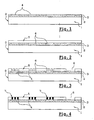
- Figure 1 shows a starting point in the process according to the invention. It shows a plate 0 including a silicium chip 1 on which are arranged circuits 2. A passivation layer 3 is superimposed on the layer including circuits 2. In this passivation layer 3 there are contact pads 4 inserted with the purpose to arrange interconnection with an additional circuit.
- Figure 2 shows the first stage, in the process, actually a stage of laying down an organic layer 5 with adhesive properties.
- This organic layer is superimposed on the passivation layer 3 including contact pads 4.
- This organic layer is for instance laid in the form of a solution obtained by centrifuging.
- organic matter 5 is removed partially or completely, and this in particular over the contact pads 4. This matter removal may be achieved for instance by etching. If the organic matter is photosensitive, it may be also exposed, after applying a masker, to rays and in particular to UV rays. The parts of organic matter exposed are finally dissolved using a chemical bath. The organic layer 5 so modified is said to be formed into a structure.
- Figure 4 shows the following stage which is a stage of growth for small metal sticks 7 in the areas where the organic matter has been removed.
- This metal stick growth is achieved for instance in chemical baths using electroless or electrochemistry.
- the small metal sticks 7 are directed preferably perpendicular to the contact pad surface 4 and are insulated from each other by the organic matter in layer 5.
- figure 4 suggests the existence of small metal sticks 7 at the level of the contact pads 4, this does not exclude the possibility to also grow some in other areas.
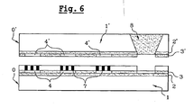
- the following stage is a stage to align a second plate 0' of the same type as plate 0 on the first plate 0 so that the contact pads 4 and 4' face each other.
- This second plate may include circuits 2' necessary for the operation of circuits 2.
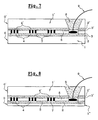
- both plates 0 and 0' are fixed, for example, using thermo-compression. Ultrasound techniques may also be used advantageously.
- Plate 0' includes media 8 so as to allow the electrical contacts 4 to exit to the outside by means, for instance, of the wiring cable 9 as can be seen on figure 7 .
- Figure 8 shows that it is possible to proceed next to the plate 0 tapering at the level of its lower face 1" in order, for instance, to enable a possible slip sheet inserting into a card body or so as to increase the difficulty in separating circuits for safety.
- the subject of this invention may apply not only to the field of mechanical and electrical connections at the level of a component or an integrated circuit, but also at the level of any other electrical device with a face equipped with contact pads. It may be in particular a question of wafers of any size, for example with a diameter of 150 mm and comprising approximately one thousand components.
- any material with adhesive properties may be used.
- This may be in particular polyimides, photosensitive resins or thermoplastics. These materials also have the advantage of stimulating the growth of metal compounds.
- thermoplastics is interesting since it will be possible to separate without damage the two electrical elements.
- the polyimides will be used with an advantage whenever it is intended to make difficult the separation of the two components without physical damage. This is particularly interesting in the field of memory cards regarding physical security.
- the small metal sticks 7 may be more generally metal compounds, for example compounds with nickel, palladium or copper.
- the metal contact structure (4,7,4') according to this invention avoids what is called contact recovery. This is because on the market wafers, localised oxidation patches often exist on contact pads, that are generally in aluminium. The contact recovery consists in cleaning these contact pads to remove the oxidation so as to have good quality electrical connections.
- the contact structure according to this invention (4,7,4') especially because of the number and the reduced size of the cross-section of small metal sticks 7 in relation to the size of the oxidation patches, enables eliminating this stage called contact recovery.
- conductive paths 7 shown on figure 7 have a height greater than the thickness of the organic layer 5, so that when fixing, there is a good interpenetration of these paths in the metal of the contact pads 4' of the second plate 0'.
- these pads are aluminium and are about 1 ⁇ m thick.
- a multi-layer may also improve the quality of fixing via a better planishing of the circuit surface or a look for a better chemical reactivity.
- the plate After the growth of metal small sticks in the organic layer 5 which acts as the fixing layer, the plate may be divided into smaller electrical entities, for instance integrated circuits or components. These electrical entities may then be mounted using the technique called Flip chip.
- the material in the organic layer is used as the adhesive agent on the support. It is thus possible to get connections in the order of 10 ⁇ m instead of the 40 to 60 ⁇ m obtained using the flip chip technique. This reduction in the connection size is especially advantageous in the field of high frequencies.
Landscapes
- Wire Bonding (AREA)
- Internal Circuitry In Semiconductor Integrated Circuit Devices (AREA)
- Connections Effected By Soldering, Adhesion, Or Permanent Deformation (AREA)
- Multi-Conductor Connections (AREA)
- Electric Connection Of Electric Components To Printed Circuits (AREA)
- Manufacturing Of Electrical Connectors (AREA)
Description
- This invention concerns the electrical and mechanical connection of an electrical device with another electrical device. Both could be for example a wafer, an integrated circuit or even just a component. This invention applies especially to the field of integrated circuits protection and in particular in the field of memory cards.
- A connection process is based on the use of a film called ACF (Anisotropic Conductor Film). This type of film contains conducting elements extending through the film thickness. According to a first stage, the film is made separately onto a neutral support. According to a second stage, the film is finely recovered using sub-engraving. According to a third stage, the film is pasted with glue on each face to apply it then onto a first component. A last stage consists in connecting a second component onto the part of the film that is not yet covered. Finally, both components are fixed mechanically through the glue pasted on both faces of the film, and electrically using the metal elements enclosed in the film.
-
US 6,256,874 describes a method for connecting two conductive layers in an electronic circuit package comprising the steps of forming dentrites on selected regions of a first conductive layer, forming dentrites on selected regions of a second conductive layer. Dentrites are formed by means of a photoresist material to the area of a first surface metal and then expose and develop the resist by photolithographic techniques to provide an exposed area on which dentrites are to be formed. The photoresist is then removed. The method further comprises the step of applying an epoxy adhesive material over the first conductive layer, and compressively attaching the second conductive layer to the first conductive layer such that the dentrites on the first conductive layer contact the dentrites on the second conductive layer. - An object of the invention is to reduce the costs.
- According to one aspect of the invention a method of manufacturing an electrical device that is electrically and mechanically connectable to another electrical device, the electrical device having a face equipped with contact pads, the method being defined in
claim 1. - The adhesive layer is, as it were, used as a mould to form the conductive path. Consequently there is no need for a specific photoresist layer as in
US 6,256,874 . The invention thus allows a reduction of the costs. - This invention shall be better grasped after reading the following nonlimiting description, written by reference to the attached drawings, where:
-
figure 1 shows as a cross-section, a plate which is a starting point for the invention process; -
figure 2 shows as a cross-section, a fixing organic layer applied to the plate according to a first stage in the process subject of the invention; -
figure 3 shows as a cross-section, a fixing organic layer that has been structured according to a second stage in the process subject of the invention; -
figure 4 shows the stage in the process according to the invention in which the fixing layer is equipped with small metal sticks; -
figure 5 shows, as a horizontal projection and as a cross-section, part of a plate; -
figure 6 shows the beginning of the fixing stage according to the invention process; -
figure 7 shows, as a cross-section, the plates after the stage of fixing by thermo-compression; -
figure 8 shows, as a cross-section, the first-plate tapering. -
Figure 1 shows a starting point in the process according to the invention. It shows aplate 0 including asilicium chip 1 on which are arrangedcircuits 2. Apassivation layer 3 is superimposed on thelayer including circuits 2. In thispassivation layer 3 there arecontact pads 4 inserted with the purpose to arrange interconnection with an additional circuit. -
Figure 2 shows the first stage, in the process, actually a stage of laying down anorganic layer 5 with adhesive properties. This organic layer is superimposed on thepassivation layer 3 includingcontact pads 4. This organic layer is for instance laid in the form of a solution obtained by centrifuging. - After a drying stage, and as shown by
figure 3 ,organic matter 5 is removed partially or completely, and this in particular over thecontact pads 4. This matter removal may be achieved for instance by etching. If the organic matter is photosensitive, it may be also exposed, after applying a masker, to rays and in particular to UV rays. The parts of organic matter exposed are finally dissolved using a chemical bath. Theorganic layer 5 so modified is said to be formed into a structure. -
Figure 4 shows the following stage which is a stage of growth forsmall metal sticks 7 in the areas where the organic matter has been removed. This metal stick growth is achieved for instance in chemical baths using electroless or electrochemistry. Thesmall metal sticks 7 are directed preferably perpendicular to thecontact pad surface 4 and are insulated from each other by the organic matter inlayer 5. Althoughfigure 4 suggests the existence ofsmall metal sticks 7 at the level of thecontact pads 4, this does not exclude the possibility to also grow some in other areas. - The following stage, as shown in
figure 6 , is a stage to align a second plate 0' of the same type asplate 0 on thefirst plate 0 so that thecontact pads 4 and 4' face each other. This second plate may include circuits 2' necessary for the operation ofcircuits 2. - In a later stage, as described in
figure 7 , bothplates 0 and 0' are fixed, for example, using thermo-compression. Ultrasound techniques may also be used advantageously. - Plate 0' includes
media 8 so as to allow theelectrical contacts 4 to exit to the outside by means, for instance, of thewiring cable 9 as can be seen onfigure 7 . -
Figure 8 shows that it is possible to proceed next to theplate 0 tapering at the level of itslower face 1" in order, for instance, to enable a possible slip sheet inserting into a card body or so as to increase the difficulty in separating circuits for safety. - Of course, the description of the invention embodiment as given above is not limiting for the invention which must be understood broadly.
- In particular, the subject of this invention may apply not only to the field of mechanical and electrical connections at the level of a component or an integrated circuit, but also at the level of any other electrical device with a face equipped with contact pads. It may be in particular a question of wafers of any size, for example with a diameter of 150 mm and comprising approximately one thousand components.
- Regarding the
organic layer 5, any material with adhesive properties, may be used. This may be in particular polyimides, photosensitive resins or thermoplastics. These materials also have the advantage of stimulating the growth of metal compounds.
The use of thermoplastics is interesting since it will be possible to separate without damage the two electrical elements. On the other hand, the polyimides will be used with an advantage whenever it is intended to make difficult the separation of the two components without physical damage. This is particularly interesting in the field of memory cards regarding physical security. - The
small metal sticks 7 may be more generally metal compounds, for example compounds with nickel, palladium or copper. - As can be seen in
figures 4 and5 , severalsmall metal sticks 7 are grown percontact area 4, typically about ten. This allows relatively good quality electrical contacts. The metal small sticks diameter is between, for example, 10 and 30 µm.
The metal contact structure (4,7,4') according to this invention avoids what is called contact recovery. This is because on the market wafers, localised oxidation patches often exist on contact pads, that are generally in aluminium. The contact recovery consists in cleaning these contact pads to remove the oxidation so as to have good quality electrical connections. However the contact structure according to this invention (4,7,4'), especially because of the number and the reduced size of the cross-section ofsmall metal sticks 7 in relation to the size of the oxidation patches, enables eliminating this stage called contact recovery.
Let us assume for instance that, at the level of a certain contact pad, there are 25 metal small sticks. Let us assume also that there is an oxidation patch that prevents 10 of these 25 small sticks to be in contact with the contact pad. In this case, there remains 15 metal small sticks in contact and ensuring however a rather good electrical connection between the electrical devices. - In the invention, in particular, when fixing by thermo-compression, it is necessary that
conductive paths 7 shown onfigure 7 have a height greater than the thickness of theorganic layer 5, so that when fixing, there is a good interpenetration of these paths in the metal of the contact pads 4' of the second plate 0'. Generally, these pads are aluminium and are about 1 µm thick. - Also other modes of embodiment are likely to give results that are particularly interesting.
- At the interface fixing level (5,7), several layers of composite materials may be used. An intermediary layer may be used to rearrange the
contact areas 4 on the interface (5,7). Further to structuring a first organic layer, metal tracks may be created by deposition. A second structured organic layer may again be used for the growth of metallic compounds.
Several layers analogous to theorganic layer 5 may be used in this way, either to create conducting media, or to create metal tracks. The last stage remains the stage of the electrical and mechanical connection with the second electrical device.
Several layers, analogous to theorganic layer 5, may also be used to improve the security and the complexity of the interface. A multi-layer may also improve the quality of fixing via a better planishing of the circuit surface or a look for a better chemical reactivity. - After the growth of metal small sticks in the
organic layer 5 which acts as the fixing layer, the plate may be divided into smaller electrical entities, for instance integrated circuits or components. These electrical entities may then be mounted using the technique called Flip chip. The material in the organic layer is used as the adhesive agent on the support. It is thus possible to get connections in the order of 10 µm instead of the 40 to 60 µm obtained using the flip chip technique. This reduction in the connection size is especially advantageous in the field of high frequencies.
Claims (6)
- A method of manufacturing an electrical device that is electrically and mechanically connectable to another electrical device, the electrical device having a face equipped with contact pads, the method including:- a layer-application step in which an organic layer is applied on the face equipped with contact pads, the organic layer being composed of a substance with adhesive properties;- an opening-creation step in which a plurality of openings are created through the organic layer over each contact pad;- a growth step in which metal sticks are electrolessly or electrochemically grown in the openings so as to form a plurality of conductive paths over each contact pad, characterized in that the height of each stick is greater than thickness of the organic layer.
- The method according to claim 1 characterised in that the organic layer is a polyimide.
- A method to electrically and mechanically connect a first electrical device and a second electrical device, each device having a face equipped with contact pads, the method being characterised in that it includes:- a first step for forming the first electrical device according to the method of claim 1; and- a device connection step, in which the said organic layer is brought into contact with the said face of the second electrical device, such that each plurality of conductive paths makes an electrical connection between a contact pad of the first electrical device and a contact pad of the second electrical device.
- A method to electrically and mechanically connect a first wafer and a second wafer, each wafer having a face equipped with contact pads, the method including:- a layer-application step in which an organic layer is applied on the face equipped with contact pads of the first wafer, the organic layer being composed of a substance with adhesive properties;- an opening-creation step in which a plurality of openings are created through the organic layer over each contact pads;- a growth step in which metal sticks are electrolessly or electrochemically grown in the openings so as to form a plurality of conductive paths over each contact pad, the height of each stick being greater than the thickness of the organic layer;- a device connection step, in which the organic layer is placed into contact with the said face of the second wafer, such that each plurality of conductive paths makes an electrical connection between a contact pad of the first wafer and a contact pad of the second wafer; and- a cutting step in which the two wafers so connected are cut into smaller electrical entities.
- An electrical device that is electrically and mechanically connectable to another electrical device, the electrical device having a face equipped with contact pads, and comprising an organic layer on said face, the organic layer having an adhesive property and comprising a plurality of conductive paths formed in a plurality of openings over each contact pad, the openings extending through the organic layer to the contact pads and in which a plurality of metal sticks have been electrolessly or electrochemically grown, characterized in that the sticks have a height greater than the thickness of organic layer.
- An electrical assembly comprising a first electrical device and a second electrical device, the first device and the second device each having a face equipped with contact pads and being electrically connected to each other the devices being stuck together by means of an organic layer composed of a substance with adhesive properties formed on the first electrical device, the assembly being characterised in that the organic layer comprises a plurality of conductive paths per contact pad formed by a plurality of openings that extend through the organic layer and in which a plurality of metal sticks have been electrolessly or electrochemically grown and wherein the conductive paths have a height higher than the thickness of the organic layer before the first and second electrical devices are stuck together.
Applications Claiming Priority (3)
| Application Number | Priority Date | Filing Date | Title |
|---|---|---|---|
| FR0110483 | 2001-08-03 | ||
| FR0110483A FR2828334A1 (en) | 2001-08-03 | 2001-08-03 | METHOD FOR MAKING AN ELECTRICAL AND MECHANICAL CONNECTION AN ELECTRICAL DEVICE HAVING A FACE PROVIDED WITH CONTACTS |
| PCT/IB2002/003041 WO2003015153A2 (en) | 2001-08-03 | 2002-08-02 | Process to allow electrical and mechanical connection of an electrical device with a face equipped with contact pads |
Publications (2)
| Publication Number | Publication Date |
|---|---|
| EP1421614A2 EP1421614A2 (en) | 2004-05-26 |
| EP1421614B1 true EP1421614B1 (en) | 2015-02-25 |
Family
ID=8866302
Family Applications (1)
| Application Number | Title | Priority Date | Filing Date |
|---|---|---|---|
| EP02751499.1A Expired - Lifetime EP1421614B1 (en) | 2001-08-03 | 2002-08-02 | Process to allow electrical and mechanical connection of an electrical device with a face equipped with contact pads |
Country Status (8)
| Country | Link |
|---|---|
| US (2) | US8429813B2 (en) |
| EP (1) | EP1421614B1 (en) |
| JP (1) | JP2005526374A (en) |
| KR (1) | KR100934862B1 (en) |
| CN (2) | CN101872753B (en) |
| AU (1) | AU2002355496A1 (en) |
| FR (1) | FR2828334A1 (en) |
| WO (1) | WO2003015153A2 (en) |
Families Citing this family (3)
| Publication number | Priority date | Publication date | Assignee | Title |
|---|---|---|---|---|
| FR2866753B1 (en) * | 2004-02-25 | 2006-06-09 | Commissariat Energie Atomique | MICROELECTRONIC INTERCONNECTION DEVICE WITH LOCALIZED CONDUCTIVE RODS |
| FR3078823B1 (en) * | 2018-03-12 | 2020-02-21 | Commissariat A L'energie Atomique Et Aux Energies Alternatives | 3D STACK OF ELECTRONIC CHIPS |
| US20220084884A1 (en) | 2020-09-15 | 2022-03-17 | Nanya Technology Corporation | Semiconductor structure and method of forming the same |
Family Cites Families (25)
| Publication number | Priority date | Publication date | Assignee | Title |
|---|---|---|---|---|
| US4008300A (en) * | 1974-10-15 | 1977-02-15 | A & P Products Incorporated | Multi-conductor element and method of making same |
| US4574095A (en) * | 1984-11-19 | 1986-03-04 | International Business Machines Corporation | Selective deposition of copper |
| US4897338A (en) * | 1987-08-03 | 1990-01-30 | Allied-Signal Inc. | Method for the manufacture of multilayer printed circuit boards |
| JPS6468935A (en) * | 1987-09-09 | 1989-03-15 | Ricoh Kk | Face-down bonding of semiconductor integrated circuit device |
| US4941255A (en) * | 1989-11-15 | 1990-07-17 | Eastman Kodak Company | Method for precision multichip assembly |
| US5151168A (en) * | 1990-09-24 | 1992-09-29 | Micron Technology, Inc. | Process for metallizing integrated circuits with electrolytically-deposited copper |
| US5543585A (en) * | 1994-02-02 | 1996-08-06 | International Business Machines Corporation | Direct chip attachment (DCA) with electrically conductive adhesives |
| US5501755A (en) * | 1994-02-18 | 1996-03-26 | Minnesota Mining And Manufacturing Company | Large area multi-electrode radiation detector substrate |
| US5659952A (en) * | 1994-09-20 | 1997-08-26 | Tessera, Inc. | Method of fabricating compliant interface for semiconductor chip |
| KR0138295B1 (en) * | 1994-11-30 | 1998-06-01 | 김광호 | How to form conductive line |
| US5674787A (en) * | 1996-01-16 | 1997-10-07 | Sematech, Inc. | Selective electroless copper deposited interconnect plugs for ULSI applications |
| US5717475A (en) * | 1996-01-30 | 1998-02-10 | Canon Kabushiki Kaisha | Electrode substrate, process for producing the substrate, liquid crystal device and process for producing the device |
| JPH10321667A (en) | 1997-05-16 | 1998-12-04 | Ricoh Co Ltd | Semiconductor device |
| US6300575B1 (en) * | 1997-08-25 | 2001-10-09 | International Business Machines Corporation | Conductor interconnect with dendrites through film |
| JP3068534B2 (en) | 1997-10-14 | 2000-07-24 | 九州日本電気株式会社 | Semiconductor device |
| DE19800566A1 (en) * | 1998-01-09 | 1999-07-15 | Siemens Ag | Method for producing a semiconductor component and a semiconductor component produced in this way |
| US6025638A (en) * | 1998-06-01 | 2000-02-15 | International Business Machines Corporation | Structure for precision multichip assembly |
| JP3413120B2 (en) * | 1999-02-23 | 2003-06-03 | ローム株式会社 | Semiconductor device with chip-on-chip structure |
| JP2000286549A (en) * | 1999-03-24 | 2000-10-13 | Fujitsu Ltd | Method for manufacturing substrate with via connection |
| FR2792440B1 (en) * | 1999-04-19 | 2001-06-08 | Schlumberger Systems & Service | DEVICE WITH SECURE INTEGRATED CIRCUIT AGAINST ATTACKS PROCEDED BY CONTROLLED DESTRUCTION OF A COMPLEMENTARY LAYER |
| JP2001015556A (en) * | 1999-07-02 | 2001-01-19 | Casio Comput Co Ltd | Semiconductor device, its manufacturing method and its mounting structure |
| US6350664B1 (en) * | 1999-09-02 | 2002-02-26 | Matsushita Electric Industrial Co., Ltd. | Semiconductor device and method of manufacturing the same |
| US7211512B1 (en) * | 2000-01-18 | 2007-05-01 | Micron Technology, Inc. | Selective electroless-plated copper metallization |
| US6834426B1 (en) * | 2000-07-25 | 2004-12-28 | International Business Machines Corporation | Method of fabricating a laminate circuit structure |
| US6627477B1 (en) * | 2000-09-07 | 2003-09-30 | International Business Machines Corporation | Method of assembling a plurality of semiconductor devices having different thickness |
-
2001
- 2001-08-03 FR FR0110483A patent/FR2828334A1/en active Pending
-
2002
- 2002-08-02 CN CN200910205384XA patent/CN101872753B/en not_active Expired - Fee Related
- 2002-08-02 WO PCT/IB2002/003041 patent/WO2003015153A2/en not_active Ceased
- 2002-08-02 CN CN028195388A patent/CN1565053B/en not_active Expired - Fee Related
- 2002-08-02 US US10/485,693 patent/US8429813B2/en not_active Expired - Fee Related
- 2002-08-02 KR KR1020047001685A patent/KR100934862B1/en not_active Expired - Fee Related
- 2002-08-02 JP JP2003519986A patent/JP2005526374A/en active Pending
- 2002-08-02 AU AU2002355496A patent/AU2002355496A1/en not_active Abandoned
- 2002-08-02 EP EP02751499.1A patent/EP1421614B1/en not_active Expired - Lifetime
-
2010
- 2010-03-01 US US12/714,719 patent/US8508952B2/en not_active Expired - Fee Related
Also Published As
| Publication number | Publication date |
|---|---|
| WO2003015153A2 (en) | 2003-02-20 |
| KR100934862B1 (en) | 2009-12-31 |
| US20100157555A1 (en) | 2010-06-24 |
| KR20040030921A (en) | 2004-04-09 |
| US8429813B2 (en) | 2013-04-30 |
| US8508952B2 (en) | 2013-08-13 |
| CN101872753B (en) | 2013-01-30 |
| WO2003015153A3 (en) | 2004-03-11 |
| AU2002355496A1 (en) | 2003-02-24 |
| FR2828334A1 (en) | 2003-02-07 |
| CN1565053B (en) | 2010-05-26 |
| HK1068730A1 (en) | 2005-04-29 |
| JP2005526374A (en) | 2005-09-02 |
| EP1421614A2 (en) | 2004-05-26 |
| CN101872753A (en) | 2010-10-27 |
| CN1565053A (en) | 2005-01-12 |
| US20050034303A1 (en) | 2005-02-17 |
Similar Documents
| Publication | Publication Date | Title |
|---|---|---|
| EP1503409B1 (en) | Module with embedded semiconductor IC which has a narrow electrode pitch and method of fabricating the module | |
| US5998291A (en) | Attachment method for assembly of high density multiple interconnect structures | |
| US6569712B2 (en) | Structure of a ball-grid array package substrate and processes for producing thereof | |
| US8859077B2 (en) | Method of manufacturing multilayer wiring substrate, and multilayer wiring substrate | |
| EP1656006A1 (en) | A substrate having high electrical connection reliability of a penetrating via connected to wirings and a method for manufacturing the same | |
| US20140215782A1 (en) | Multilayer wiring substrate, and method of manufacturing the same | |
| KR100896810B1 (en) | Printed Circuit Board and Manufacturing Method | |
| CN113223971A (en) | Semiconductor device and method of manufacturing the same | |
| JP2002314257A (en) | Multilayer circuit board, manufacturing method thereof and electric assembly | |
| EP2040294A1 (en) | Method of manufacturing a semiconductor device | |
| JP2002313996A (en) | Semiconductor package substrate and method of manufacturing the same | |
| KR20090071444A (en) | Manufacturing Method of Semiconductor Device | |
| US8508952B2 (en) | Electrical assembly | |
| US20140263582A1 (en) | Low cost interposer and method of fabrication | |
| EP2071622A2 (en) | Package for semiconductor device and method of manufacturing the same | |
| JP5982760B2 (en) | Electronic device and manufacturing method thereof | |
| US20060030140A1 (en) | Method of making bondable leads using positive photoresist and structures made therefrom | |
| US6210746B1 (en) | Method of fabricating a solder resist mask | |
| KR101067063B1 (en) | Carrier for manufacturing printed circuit board, manufacturing method thereof and manufacturing method of printed circuit board using same | |
| JP4286264B2 (en) | Semiconductor device and manufacturing method thereof | |
| HK1068730B (en) | Process to allow electrical and mechanical connection of an electrical device with a face equipped with contact pads | |
| JP4392201B2 (en) | Electronic device and manufacturing method thereof | |
| KR0186208B1 (en) | Bump structure | |
| JP2006120932A (en) | Method for forming through wiring on substrate | |
| JP2001358173A (en) | Semiconductor device and its manufacturing method, circuit board, and electronic equipment |
Legal Events
| Date | Code | Title | Description |
|---|---|---|---|
| PUAI | Public reference made under article 153(3) epc to a published international application that has entered the european phase |
Free format text: ORIGINAL CODE: 0009012 |
|
| 17P | Request for examination filed |
Effective date: 20040302 |
|
| AK | Designated contracting states |
Kind code of ref document: A2 Designated state(s): AT BE BG CH CY CZ DE DK EE ES FI FR GB GR IE IT LI LU MC NL PT SE SK TR |
|
| AX | Request for extension of the european patent |
Extension state: AL LT LV MK RO SI |
|
| RAP1 | Party data changed (applicant data changed or rights of an application transferred) |
Owner name: SCHLUMBERGER MALCO, INC. Owner name: AXALTO S.A. |
|
| RAP1 | Party data changed (applicant data changed or rights of an application transferred) |
Owner name: GEMALTO SA Owner name: SCHLUMBERGER MALCO, INC. |
|
| 17Q | First examination report despatched |
Effective date: 20110530 |
|
| GRAP | Despatch of communication of intention to grant a patent |
Free format text: ORIGINAL CODE: EPIDOSNIGR1 |
|
| RIC1 | Information provided on ipc code assigned before grant |
Ipc: H01L 23/00 20060101ALI20140924BHEP Ipc: H01L 21/56 20060101ALI20140924BHEP Ipc: H01L 21/60 20060101AFI20140924BHEP |
|
| INTG | Intention to grant announced |
Effective date: 20141022 |
|
| GRAS | Grant fee paid |
Free format text: ORIGINAL CODE: EPIDOSNIGR3 |
|
| GRAA | (expected) grant |
Free format text: ORIGINAL CODE: 0009210 |
|
| AK | Designated contracting states |
Kind code of ref document: B1 Designated state(s): AT BE BG CH CY CZ DE DK EE ES FI FR GB GR IE IT LI LU MC NL PT SE SK TR |
|
| REG | Reference to a national code |
Ref country code: GB Ref legal event code: FG4D |
|
| REG | Reference to a national code |
Ref country code: CH Ref legal event code: EP |
|
| REG | Reference to a national code |
Ref country code: IE Ref legal event code: FG4D |
|
| REG | Reference to a national code |
Ref country code: DE Ref legal event code: R096 Ref document number: 60246987 Country of ref document: DE Effective date: 20150409 |
|
| REG | Reference to a national code |
Ref country code: AT Ref legal event code: REF Ref document number: 712628 Country of ref document: AT Kind code of ref document: T Effective date: 20150415 |
|
| REG | Reference to a national code |
Ref country code: NL Ref legal event code: VDEP Effective date: 20150225 |
|
| REG | Reference to a national code |
Ref country code: AT Ref legal event code: MK05 Ref document number: 712628 Country of ref document: AT Kind code of ref document: T Effective date: 20150225 |
|
| REG | Reference to a national code |
Ref country code: FR Ref legal event code: PLFP Year of fee payment: 14 |
|
| PG25 | Lapsed in a contracting state [announced via postgrant information from national office to epo] |
Ref country code: SE Free format text: LAPSE BECAUSE OF FAILURE TO SUBMIT A TRANSLATION OF THE DESCRIPTION OR TO PAY THE FEE WITHIN THE PRESCRIBED TIME-LIMIT Effective date: 20150225 Ref country code: ES Free format text: LAPSE BECAUSE OF FAILURE TO SUBMIT A TRANSLATION OF THE DESCRIPTION OR TO PAY THE FEE WITHIN THE PRESCRIBED TIME-LIMIT Effective date: 20150225 Ref country code: FI Free format text: LAPSE BECAUSE OF FAILURE TO SUBMIT A TRANSLATION OF THE DESCRIPTION OR TO PAY THE FEE WITHIN THE PRESCRIBED TIME-LIMIT Effective date: 20150225 |
|
| PG25 | Lapsed in a contracting state [announced via postgrant information from national office to epo] |
Ref country code: AT Free format text: LAPSE BECAUSE OF FAILURE TO SUBMIT A TRANSLATION OF THE DESCRIPTION OR TO PAY THE FEE WITHIN THE PRESCRIBED TIME-LIMIT Effective date: 20150225 Ref country code: GR Free format text: LAPSE BECAUSE OF FAILURE TO SUBMIT A TRANSLATION OF THE DESCRIPTION OR TO PAY THE FEE WITHIN THE PRESCRIBED TIME-LIMIT Effective date: 20150526 |
|
| PG25 | Lapsed in a contracting state [announced via postgrant information from national office to epo] |
Ref country code: NL Free format text: LAPSE BECAUSE OF FAILURE TO SUBMIT A TRANSLATION OF THE DESCRIPTION OR TO PAY THE FEE WITHIN THE PRESCRIBED TIME-LIMIT Effective date: 20150225 |
|
| PG25 | Lapsed in a contracting state [announced via postgrant information from national office to epo] |
Ref country code: CZ Free format text: LAPSE BECAUSE OF FAILURE TO SUBMIT A TRANSLATION OF THE DESCRIPTION OR TO PAY THE FEE WITHIN THE PRESCRIBED TIME-LIMIT Effective date: 20150225 Ref country code: EE Free format text: LAPSE BECAUSE OF FAILURE TO SUBMIT A TRANSLATION OF THE DESCRIPTION OR TO PAY THE FEE WITHIN THE PRESCRIBED TIME-LIMIT Effective date: 20150225 Ref country code: DK Free format text: LAPSE BECAUSE OF FAILURE TO SUBMIT A TRANSLATION OF THE DESCRIPTION OR TO PAY THE FEE WITHIN THE PRESCRIBED TIME-LIMIT Effective date: 20150225 Ref country code: SK Free format text: LAPSE BECAUSE OF FAILURE TO SUBMIT A TRANSLATION OF THE DESCRIPTION OR TO PAY THE FEE WITHIN THE PRESCRIBED TIME-LIMIT Effective date: 20150225 |
|
| REG | Reference to a national code |
Ref country code: DE Ref legal event code: R097 Ref document number: 60246987 Country of ref document: DE |
|
| PLBE | No opposition filed within time limit |
Free format text: ORIGINAL CODE: 0009261 |
|
| STAA | Information on the status of an ep patent application or granted ep patent |
Free format text: STATUS: NO OPPOSITION FILED WITHIN TIME LIMIT |
|
| 26N | No opposition filed |
Effective date: 20151126 |
|
| PG25 | Lapsed in a contracting state [announced via postgrant information from national office to epo] |
Ref country code: LU Free format text: LAPSE BECAUSE OF FAILURE TO SUBMIT A TRANSLATION OF THE DESCRIPTION OR TO PAY THE FEE WITHIN THE PRESCRIBED TIME-LIMIT Effective date: 20150802 Ref country code: MC Free format text: LAPSE BECAUSE OF FAILURE TO SUBMIT A TRANSLATION OF THE DESCRIPTION OR TO PAY THE FEE WITHIN THE PRESCRIBED TIME-LIMIT Effective date: 20150225 |
|
| REG | Reference to a national code |
Ref country code: CH Ref legal event code: PL |
|
| PG25 | Lapsed in a contracting state [announced via postgrant information from national office to epo] |
Ref country code: CH Free format text: LAPSE BECAUSE OF NON-PAYMENT OF DUE FEES Effective date: 20150831 Ref country code: LI Free format text: LAPSE BECAUSE OF NON-PAYMENT OF DUE FEES Effective date: 20150831 |
|
| PG25 | Lapsed in a contracting state [announced via postgrant information from national office to epo] |
Ref country code: BE Free format text: LAPSE BECAUSE OF FAILURE TO SUBMIT A TRANSLATION OF THE DESCRIPTION OR TO PAY THE FEE WITHIN THE PRESCRIBED TIME-LIMIT Effective date: 20150225 |
|
| REG | Reference to a national code |
Ref country code: IE Ref legal event code: MM4A |
|
| REG | Reference to a national code |
Ref country code: FR Ref legal event code: PLFP Year of fee payment: 15 |
|
| PG25 | Lapsed in a contracting state [announced via postgrant information from national office to epo] |
Ref country code: IE Free format text: LAPSE BECAUSE OF NON-PAYMENT OF DUE FEES Effective date: 20150802 |
|
| PG25 | Lapsed in a contracting state [announced via postgrant information from national office to epo] |
Ref country code: BG Free format text: LAPSE BECAUSE OF FAILURE TO SUBMIT A TRANSLATION OF THE DESCRIPTION OR TO PAY THE FEE WITHIN THE PRESCRIBED TIME-LIMIT Effective date: 20150225 |
|
| PG25 | Lapsed in a contracting state [announced via postgrant information from national office to epo] |
Ref country code: CY Free format text: LAPSE BECAUSE OF FAILURE TO SUBMIT A TRANSLATION OF THE DESCRIPTION OR TO PAY THE FEE WITHIN THE PRESCRIBED TIME-LIMIT Effective date: 20150225 |
|
| REG | Reference to a national code |
Ref country code: FR Ref legal event code: PLFP Year of fee payment: 16 |
|
| PG25 | Lapsed in a contracting state [announced via postgrant information from national office to epo] |
Ref country code: TR Free format text: LAPSE BECAUSE OF FAILURE TO SUBMIT A TRANSLATION OF THE DESCRIPTION OR TO PAY THE FEE WITHIN THE PRESCRIBED TIME-LIMIT Effective date: 20150225 |
|
| PG25 | Lapsed in a contracting state [announced via postgrant information from national office to epo] |
Ref country code: PT Free format text: LAPSE BECAUSE OF FAILURE TO SUBMIT A TRANSLATION OF THE DESCRIPTION OR TO PAY THE FEE WITHIN THE PRESCRIBED TIME-LIMIT Effective date: 20150225 |
|
| REG | Reference to a national code |
Ref country code: FR Ref legal event code: PLFP Year of fee payment: 17 |
|
| PGFP | Annual fee paid to national office [announced via postgrant information from national office to epo] |
Ref country code: IT Payment date: 20190722 Year of fee payment: 18 Ref country code: DE Payment date: 20190722 Year of fee payment: 18 Ref country code: FR Payment date: 20190722 Year of fee payment: 18 |
|
| PGFP | Annual fee paid to national office [announced via postgrant information from national office to epo] |
Ref country code: GB Payment date: 20190722 Year of fee payment: 18 |
|
| REG | Reference to a national code |
Ref country code: DE Ref legal event code: R119 Ref document number: 60246987 Country of ref document: DE |
|
| GBPC | Gb: european patent ceased through non-payment of renewal fee |
Effective date: 20200802 |
|
| PG25 | Lapsed in a contracting state [announced via postgrant information from national office to epo] |
Ref country code: DE Free format text: LAPSE BECAUSE OF NON-PAYMENT OF DUE FEES Effective date: 20210302 Ref country code: IT Free format text: LAPSE BECAUSE OF NON-PAYMENT OF DUE FEES Effective date: 20200802 Ref country code: FR Free format text: LAPSE BECAUSE OF NON-PAYMENT OF DUE FEES Effective date: 20200831 |
|
| PG25 | Lapsed in a contracting state [announced via postgrant information from national office to epo] |
Ref country code: GB Free format text: LAPSE BECAUSE OF NON-PAYMENT OF DUE FEES Effective date: 20200802 |