EP1417517B1 - Optische einrichtung und verfahren zur herstellung - Google Patents
Optische einrichtung und verfahren zur herstellung Download PDFInfo
- Publication number
- EP1417517B1 EP1417517B1 EP02721837A EP02721837A EP1417517B1 EP 1417517 B1 EP1417517 B1 EP 1417517B1 EP 02721837 A EP02721837 A EP 02721837A EP 02721837 A EP02721837 A EP 02721837A EP 1417517 B1 EP1417517 B1 EP 1417517B1
- Authority
- EP
- European Patent Office
- Prior art keywords
- pixel
- image
- optically
- resist
- optical device
- Prior art date
- Legal status (The legal status is an assumption and is not a legal conclusion. Google has not performed a legal analysis and makes no representation as to the accuracy of the status listed.)
- Revoked
Links
Images


Classifications
-
- B—PERFORMING OPERATIONS; TRANSPORTING
- B42—BOOKBINDING; ALBUMS; FILES; SPECIAL PRINTED MATTER
- B42D—BOOKS; BOOK COVERS; LOOSE LEAVES; PRINTED MATTER CHARACTERISED BY IDENTIFICATION OR SECURITY FEATURES; PRINTED MATTER OF SPECIAL FORMAT OR STYLE NOT OTHERWISE PROVIDED FOR; DEVICES FOR USE THEREWITH AND NOT OTHERWISE PROVIDED FOR; MOVABLE-STRIP WRITING OR READING APPARATUS
- B42D25/00—Information-bearing cards or sheet-like structures characterised by identification or security features; Manufacture thereof
- B42D25/30—Identification or security features, e.g. for preventing forgery
- B42D25/328—Diffraction gratings; Holograms
-
- B—PERFORMING OPERATIONS; TRANSPORTING
- B42—BOOKBINDING; ALBUMS; FILES; SPECIAL PRINTED MATTER
- B42D—BOOKS; BOOK COVERS; LOOSE LEAVES; PRINTED MATTER CHARACTERISED BY IDENTIFICATION OR SECURITY FEATURES; PRINTED MATTER OF SPECIAL FORMAT OR STYLE NOT OTHERWISE PROVIDED FOR; DEVICES FOR USE THEREWITH AND NOT OTHERWISE PROVIDED FOR; MOVABLE-STRIP WRITING OR READING APPARATUS
- B42D25/00—Information-bearing cards or sheet-like structures characterised by identification or security features; Manufacture thereof
- B42D25/30—Identification or security features, e.g. for preventing forgery
- B42D25/324—Reliefs
-
- B—PERFORMING OPERATIONS; TRANSPORTING
- B42—BOOKBINDING; ALBUMS; FILES; SPECIAL PRINTED MATTER
- B42D—BOOKS; BOOK COVERS; LOOSE LEAVES; PRINTED MATTER CHARACTERISED BY IDENTIFICATION OR SECURITY FEATURES; PRINTED MATTER OF SPECIAL FORMAT OR STYLE NOT OTHERWISE PROVIDED FOR; DEVICES FOR USE THEREWITH AND NOT OTHERWISE PROVIDED FOR; MOVABLE-STRIP WRITING OR READING APPARATUS
- B42D25/00—Information-bearing cards or sheet-like structures characterised by identification or security features; Manufacture thereof
- B42D25/30—Identification or security features, e.g. for preventing forgery
- B42D25/36—Identification or security features, e.g. for preventing forgery comprising special materials
- B42D25/373—Metallic materials
-
- B—PERFORMING OPERATIONS; TRANSPORTING
- B42—BOOKBINDING; ALBUMS; FILES; SPECIAL PRINTED MATTER
- B42D—BOOKS; BOOK COVERS; LOOSE LEAVES; PRINTED MATTER CHARACTERISED BY IDENTIFICATION OR SECURITY FEATURES; PRINTED MATTER OF SPECIAL FORMAT OR STYLE NOT OTHERWISE PROVIDED FOR; DEVICES FOR USE THEREWITH AND NOT OTHERWISE PROVIDED FOR; MOVABLE-STRIP WRITING OR READING APPARATUS
- B42D25/00—Information-bearing cards or sheet-like structures characterised by identification or security features; Manufacture thereof
- B42D25/40—Manufacture
- B42D25/405—Marking
- B42D25/41—Marking using electromagnetic radiation
-
- B—PERFORMING OPERATIONS; TRANSPORTING
- B42—BOOKBINDING; ALBUMS; FILES; SPECIAL PRINTED MATTER
- B42D—BOOKS; BOOK COVERS; LOOSE LEAVES; PRINTED MATTER CHARACTERISED BY IDENTIFICATION OR SECURITY FEATURES; PRINTED MATTER OF SPECIAL FORMAT OR STYLE NOT OTHERWISE PROVIDED FOR; DEVICES FOR USE THEREWITH AND NOT OTHERWISE PROVIDED FOR; MOVABLE-STRIP WRITING OR READING APPARATUS
- B42D25/00—Information-bearing cards or sheet-like structures characterised by identification or security features; Manufacture thereof
- B42D25/40—Manufacture
- B42D25/405—Marking
- B42D25/425—Marking by deformation, e.g. embossing
-
- B—PERFORMING OPERATIONS; TRANSPORTING
- B42—BOOKBINDING; ALBUMS; FILES; SPECIAL PRINTED MATTER
- B42D—BOOKS; BOOK COVERS; LOOSE LEAVES; PRINTED MATTER CHARACTERISED BY IDENTIFICATION OR SECURITY FEATURES; PRINTED MATTER OF SPECIAL FORMAT OR STYLE NOT OTHERWISE PROVIDED FOR; DEVICES FOR USE THEREWITH AND NOT OTHERWISE PROVIDED FOR; MOVABLE-STRIP WRITING OR READING APPARATUS
- B42D25/00—Information-bearing cards or sheet-like structures characterised by identification or security features; Manufacture thereof
- B42D25/40—Manufacture
- B42D25/405—Marking
- B42D25/43—Marking by removal of material
- B42D25/44—Marking by removal of material using mechanical means, e.g. engraving
-
- B—PERFORMING OPERATIONS; TRANSPORTING
- B42—BOOKBINDING; ALBUMS; FILES; SPECIAL PRINTED MATTER
- B42D—BOOKS; BOOK COVERS; LOOSE LEAVES; PRINTED MATTER CHARACTERISED BY IDENTIFICATION OR SECURITY FEATURES; PRINTED MATTER OF SPECIAL FORMAT OR STYLE NOT OTHERWISE PROVIDED FOR; DEVICES FOR USE THEREWITH AND NOT OTHERWISE PROVIDED FOR; MOVABLE-STRIP WRITING OR READING APPARATUS
- B42D25/00—Information-bearing cards or sheet-like structures characterised by identification or security features; Manufacture thereof
- B42D25/40—Manufacture
- B42D25/405—Marking
- B42D25/43—Marking by removal of material
- B42D25/445—Marking by removal of material using chemical means, e.g. etching
-
- B—PERFORMING OPERATIONS; TRANSPORTING
- B42—BOOKBINDING; ALBUMS; FILES; SPECIAL PRINTED MATTER
- B42D—BOOKS; BOOK COVERS; LOOSE LEAVES; PRINTED MATTER CHARACTERISED BY IDENTIFICATION OR SECURITY FEATURES; PRINTED MATTER OF SPECIAL FORMAT OR STYLE NOT OTHERWISE PROVIDED FOR; DEVICES FOR USE THEREWITH AND NOT OTHERWISE PROVIDED FOR; MOVABLE-STRIP WRITING OR READING APPARATUS
- B42D25/00—Information-bearing cards or sheet-like structures characterised by identification or security features; Manufacture thereof
- B42D25/40—Manufacture
- B42D25/45—Associating two or more layers
- B42D25/465—Associating two or more layers using chemicals or adhesives
- B42D25/47—Associating two or more layers using chemicals or adhesives using adhesives
-
- B—PERFORMING OPERATIONS; TRANSPORTING
- B44—DECORATIVE ARTS
- B44F—SPECIAL DESIGNS OR PICTURES
- B44F1/00—Designs or pictures characterised by special or unusual light effects
- B44F1/08—Designs or pictures characterised by special or unusual light effects characterised by colour effects
- B44F1/10—Changing, amusing, or secret pictures
-
- G—PHYSICS
- G02—OPTICS
- G02B—OPTICAL ELEMENTS, SYSTEMS OR APPARATUS
- G02B5/00—Optical elements other than lenses
- G02B5/18—Diffraction gratings
- G02B5/1861—Reflection gratings characterised by their structure, e.g. step profile, contours of substrate or grooves, pitch variations, materials
-
- G—PHYSICS
- G03—PHOTOGRAPHY; CINEMATOGRAPHY; ANALOGOUS TECHNIQUES USING WAVES OTHER THAN OPTICAL WAVES; ELECTROGRAPHY; HOLOGRAPHY
- G03C—PHOTOSENSITIVE MATERIALS FOR PHOTOGRAPHIC PURPOSES; PHOTOGRAPHIC PROCESSES, e.g. CINE, X-RAY, COLOUR, STEREO-PHOTOGRAPHIC PROCESSES; AUXILIARY PROCESSES IN PHOTOGRAPHY
- G03C8/00—Diffusion transfer processes or agents therefor; Photosensitive materials for such processes
- G03C8/42—Structural details
- G03C8/52—Bases or auxiliary layers; Substances therefor
- G03C8/56—Mordant layers
-
- B—PERFORMING OPERATIONS; TRANSPORTING
- B41—PRINTING; LINING MACHINES; TYPEWRITERS; STAMPS
- B41M—PRINTING, DUPLICATING, MARKING, OR COPYING PROCESSES; COLOUR PRINTING
- B41M3/00—Printing processes to produce particular kinds of printed work, e.g. patterns
- B41M3/06—Veined printings; Fluorescent printings; Stereoscopic images; Imitated patterns, e.g. tissues, textiles
-
- B—PERFORMING OPERATIONS; TRANSPORTING
- B41—PRINTING; LINING MACHINES; TYPEWRITERS; STAMPS
- B41M—PRINTING, DUPLICATING, MARKING, OR COPYING PROCESSES; COLOUR PRINTING
- B41M3/00—Printing processes to produce particular kinds of printed work, e.g. patterns
- B41M3/14—Security printing
- B41M3/148—Transitory images, i.e. images only visible from certain viewing angles
-
- G—PHYSICS
- G03—PHOTOGRAPHY; CINEMATOGRAPHY; ANALOGOUS TECHNIQUES USING WAVES OTHER THAN OPTICAL WAVES; ELECTROGRAPHY; HOLOGRAPHY
- G03H—HOLOGRAPHIC PROCESSES OR APPARATUS
- G03H2224/00—Writing means other than actinic light wave
- G03H2224/02—Mechanical means, e.g. diamond tool
Definitions
- This invention relates to an optical device, and in particular to an optical device which, when illuminated by a light source generates one or more images which are observable from particular ranges of viewing angles around the device.
- the device may be used in a number of different applications, and it has particular application as an anti-forgery security device on banknotes, credit cards, cheques, share certificates and other valuable documents.
- ODDs optically variable devices
- EXELGRAM TM device used to protect the new series of Hungarian banknotes and American Express US dollar and Euro travellers cheques
- KINEGRAM TM device used to protect the current series of German and Swiss banknotes.
- the EXELGRAM TM device is described in US patent numbers 5,825,547 and 6,088,161 while the KINEGRAM TM device is described in European patents EP 330,738 and EP 105099 .
- the KINEGRAM TM and EXELGRAM TM devices are examples of foil based diffractive structures that have proven to be highly effective deterrents to the counterfeiting of official documents.
- This class of optically diffractive anti-counterfeiting devices also includes the PIXELGRAM TM device that is described in European patent number EP 0 490 923 B1 and US patent number 5,428,479 .
- PIXELGRAM TM devices are manufactured by producing a counterpart diffractive structure wherein the greyness values of each pixel of an optically invariable image are mapped to corresponding small diffractive pixel regions on the PIXELGRAM TM device.
- WO-A-9823979 also discloses the state of the art.
- a more general and useful approach to the design of zero order reflective optic microstructures is obtained by utilising colour component values (such as the red, green and blue values) of each pixel in the optically invariable image and relating these parameters via a mathematical or computer algorithm to the parameters required to define the geometrical surface shape properties of each small surface region of the three dimensional reflective or diffractive microstructure.
- colour component values such as the red, green and blue values
- a method of manufacturing an optical device which generates an optically variable image the image being optically variable in that it varies according to the position of observation, the method including the steps of:
- an optical device providing an optically variable image, corresponding to an optically invariable counterpart image
- the optical device including a pixellated reflective structure which is an assembly of reflective surface relief pixels and which when illuminated generates the optically variable image, the image being optically variable in that it varies according to the position of observation, wherein each of the reflective surface relief pixels is an individual reflecting surface structure, and wherein the optically variability is produced by differing angular orientations of the individual reflective surface relief pixels.
- an optical device providing an optically variable image, corresponding to an optically invariable counterpart image, including a pixellated reflective or diffractive structure which is an assembly of zero order reflective optic surface relief pixels and which when illuminated generates an optically variable image, the image being optically variable in that it varies when viewed from different observation positions, wherein each of the zero order reflective optic pixels is an individual reflecting or diffracting three-dimensional surface structure which is directly related via a mathematical or computer algorithm to the colour component values of associated pixels of the optically invariable counterpart image.
- a method of printing an optically variable image onto a document including the steps of:
- the present invention relates to high security Optically Variable Device (OVD) microstructures and generalised reflecting or diffracting surface structures, particularly for non foil based applications where direct printing into the application substrate or direct reflection or diffraction from the replicated surface structure of the device is a specific requirement.
- OLED Optically Variable Device
- these new specialised microstructure geometries have a particular application related to direct printing onto the document via the use of specialised inks and lacquers.
- the microstructure of the OVD incorporates surface relief variations of relatively large depth dimension (eg 15 to 100 microns).
- microstructures according to the invention include the class of Zero Order Reflective Optic (ZORO) devices. These multiplexed micro-mirror array devices use reflection rather than diffraction as their fundamental OVD mechanism, and a typical OVD microstructure of this type may contain up to one million micro mirror surface regions of dimensions 30 microns X 30 microns or less with each mirror surface region designed with predetermined angle and curvature properties according to the input picture information.
- the origination of the device takes place via a multi-step process using a combination of electron beam lithography, plasma etching or wet chemical etching, photolithography and other specialised processes adopted from the semiconductor industry.
- ZORO devices include higher security and lower cost because all steps in the replication process take place within the security printing plant and there is no requirement for an off-line foil production facility.
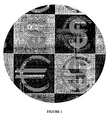
- Figure 1 shows an example of an optically invariable image comprised of multiple picture elements or pixels defined by three colour values denoting the red (R), green (G) and blue (B) components of each pixel.
- RGB colour components are used, but it is to be understood that other colour components such as CMYK or HSB are equally usable.
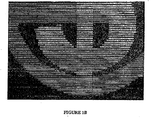
- An enlarged detail of Figure 1 is shown in Figure 1B .
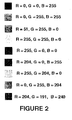
- Figure 2 shows the finite set of independent (R,G,B) values that nave been used to construct the image of Figure 1 . This set of (R,G,B) values is referred to as the RGB palette of Figure 1 .
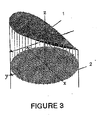
- Figure 3 shows an example of an associated micro-surface structure corresponding to a particular element of a set of (R,G,B) values.
- the micro-surface structure represent a micro-reflecting mirror structure and the R, G and B values of each optically invariable pixel determine the surface slope directions and degree of curvature of each of the corresponding micro reflecting mirror structures.
- the micro-surface pixel in this case is 30 microns in diameter.
- Figure 3 shows the micro-surface element itself 1, and the projection of the element onto the x-y plane 2.
- R 191
- the equation of the reflecting surface element is given by:
- Z R / 255 ⁇ Y + G / 255 ⁇ X 2 + B / 255 ⁇ Y 2 .
- Figure 4 shows an example of a colortone mask pixel element that generates the micro-surface relief structure shown in Figure 3 .
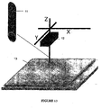
- Figure 5 shows an optical arrangement for manufacturing an optical device according to one aspect of the invention.
- UV light 3 is allowed to pass through a transparent mask 4 produced by electron beam lithography.
- the optical arrangement 5 ensures that the light 3 is then allowed to fall on and expose a surface comprised of photosensitive material 6, which in this case has a thickness of 30 micron.
- Figure 6 shows an example of a set of transparent pixel elements that can be used as a mask palette to construct a two dimensional mask containing a multiplicity of transparent mask pixels representing the optically invariable image.
- the mask When the mask is placed in front of the optical arrangement shown in figure 5 and light of short wavelengths is allowed to pass through the mask and allowed to expose the thick optical resist substrate (shown also in figure 5 ) via the optical arrangement then, upon development of the resist substrate a reflecting surface configuration is obtained corresponding to the required surface relief structure.
- the four elements in Figure 6 use the same mathematical algorithm as Figure 4 although the apertures are shown here in white rather than black as in Figure 4 . Different RGB values generate different light intensity distributions on the optical resist and therefore different pixel micro-surface geometries are formed after development of the optical resist.
- Figure 7 shows another example of a micro-surface palette function together with computer plots showing three pixel surface elements and their corresponding RGB parameter sets.
- Figure 8 shows a group of seven micro-surface palette elements belonging to the same family shown in Figure 7 . RGB values and corresponding colour patches are also shown explicitly in Figure 8 .
- Figure 9 shows the fundamental concept underpinning a key aspect of the invention.
- the same mathematical algorithm used in Figures 7 and 8 is used here to generate a small section of a surface microstructure 7 corresponding to a small section of input artwork 8.
- the small section of input artwork 8 corresponds to a particular arrangement of 36 input artwork pixels corresponding to three elements of the RGB palette.
- Figure 10 shows a small section of a diffractive optical device according to the invention and corresponding to the mapping of a set of optically invariable pixels 9 onto a corresponding set of diffraction grating microstructure elements 10.
- Figure 11 shows an example of a diffraction grating palette and corresponding RGB values for the optical device shown in Figure 10 .
- the micro-surface structure 10 represent a micro diffraction grating structure and the R, G and B values of each optically invariable pixel determine the micro diffraction grating average groove direction, spatial frequency and the curvature of the grooves within each of the corresponding micro diffraction grating structures.
- Figure 12 shows a schematic representation of an electron beam or ion beam exposure system whereby the distribution of electron or ion intensity on the resist substrate is determined by the distribution of red (R), green (G) and blue (B) colour values in the optically invariable image.
- This method of manufacturing an optical device according to the invention includes the steps of:
- Figure 13 shows a mechanical device for producing an optical device according to the invention.
- the construction of this mechanical device includes the steps of:
Landscapes
- Engineering & Computer Science (AREA)
- Manufacturing & Machinery (AREA)
- Physics & Mathematics (AREA)
- Health & Medical Sciences (AREA)
- General Health & Medical Sciences (AREA)
- Toxicology (AREA)
- Chemical & Material Sciences (AREA)
- Chemical Kinetics & Catalysis (AREA)
- General Chemical & Material Sciences (AREA)
- General Physics & Mathematics (AREA)
- Mechanical Engineering (AREA)
- Electromagnetism (AREA)
- Optics & Photonics (AREA)
- Architecture (AREA)
- Structural Engineering (AREA)
- Diffracting Gratings Or Hologram Optical Elements (AREA)
- Credit Cards Or The Like (AREA)
- Optical Integrated Circuits (AREA)
- Glass Compositions (AREA)
- Led Device Packages (AREA)
- Encapsulation Of And Coatings For Semiconductor Or Solid State Devices (AREA)
Claims (24)
- Verfahren zur Herstellung einer optischen Einrichtung, die ein optisch veränderliches Bild erzeugt, wobei das Bild insofern optisch veränderlich ist, als es sich entsprechend der Betrachtungsposition verändert, wobei das Verfahren folgende Schritte umfasst:Teilen eines optisch unveränderlichen Bildes in mehrere Pixel,Bestimmen derFarbkomponentenwerte für jeden Pixel,Bestimmen einer zugehörigen Pixel-Oberflächenstruktur fürjeden der Pixel des optisch unveränderlichen Bildes, die eine dreidimensionale Oberflächenform und -krümmung aufweist, die mittels eines mathematischen oder eines Computeralgorithmus zu den Farbkomponentenwerten des zugehörigen Pixelsin Beziehung gesetzt werden, wobei jede Pixel-Oberflächenstruktur eine individuelle, reflektierende optische Oberflächenstruktur nullter Ordnung ist, die einen sichtbaren optischen Effekt erzeugt, undErzeugen einer Anordnung der individuellen, reflektierenden optischen Oberflächenstrukturen nullter Ordnung, die bei Beleuchtung mehrere sichtbare optische Effekte erzeugt, die gemeinsam eine optisch veränderliche Reproduktion des optisch unveränderlichen Bildes bilden.
- Verfahren nach Anspruch 1, ferner folgende Schritte umfassend:(a) Bilden einer gepixelten, teilweise optisch transparente Maske durch Elektronenstrahllithographie und Plasmaätztechniken, wobei jeder Pixel der Maske eins zu eins einem Pixel im optisch unveränderlichen Bild sowie dem Grad der optischen Transparenzentspricht und wobei die Verteilung der Transparenz in jedem Maskenpixel mittels eines mathematischen oder eines Computeralgorithmus direkt zu den Farbkomponentenwerten der entsprechenden Pixel im optisch unveränderlichen Bild in Beziehung gesetzt wird,(b) Bereitstellen eines Substrats, das mit einer Schicht Photoresistmaterial beschichtet ist, wobei die Dicke des Resistsweniger als 100 Mikrometer beträgt,(c) Projizieren von Licht durch die Maske auf das Substrat, das mit der dicken Schicht Photoresist beschichtet ist, und Bestrahlen der dicken Schicht Photoresist mit einer Verteilung der Lichtstärke, welche der Verteilung der Pixeltransparenz auf der Maske entspricht, und(d) Entwickeln der bestrahlten dicken Resistschicht und Entfernen des bestrahltenResistmaterials von den belichteten Bereichen, um Veränderungen in der Dicke des Resists zu erzielen, die den Veränderungen des Oberflächenreliefs entsprechen, die für die Oberflächenstrukturen der Pixel der optischen Einrichtung erforderlich sind.
- Verfahren nach Anspruch 1, wobei das optisch unveränderliche Bild im Speicher eines Computers gespeichert wird und wobei das Verfahren ferner folgende Schritte umfasst:(a) Bereitstellen einer Metallnadel mit einem Durchmesser von 500 Mikrometern oder weniger, wobei die Nadel eine Spitze mit einer Oberfläche aufweist, die in einen, im Verhältnis zur Achse der Nadel schiefen Winkelausgerichtet ist,(b) Einführen der Nadel in eine mechanische Halterung, die an einem mechanischen Arm angebracht ist, der sich mit einem Spielraum von mindestens Grad (x, y) über eine ebene Oberfläche bewegen lässt, wobei die Spitze der Nadel zur ebenen Oberfläche hin hervorsteht, die mechanische Anordnung die Nadel unter Druck vertikal abwärts bewegt und die mechanische Anordnung außerdem die Nadel um ihre eigene Achse dreht,(c) Anbringen eines Heizelements am von der Spitze am weitesten entfernten Ende der Nadel, wobeidas Heizelement an der Spitze der Nadel eine vorbestimmte und gesteuerte Temperatur erzeugt,(d) Verbinden der mechanischen Einrichtung mit einer Steuereinrichtung, die vom Computer betrieben wird und die Nadel in einer Reihenfolge von (x, y) Positionen auf der ebenen Oberfläche bewegt und die Nadel an ausgewählten Positionen unter Druck abwärts bewegt, so dass die Nadel bis zu einer festgelegten Tiefe und in einem vorbestimmten Rotationswinkel in die Oberfläche eines reflektierenden Materials, wie etwa eine Polycarbonatplatte, eingeführt wird, wobei der Rotationswinkel der Nadel und deren Eindringtiefe in die Polycarbonatplattean einer bestimmten (x, y) Position ein Gegenstück der Darstellung der Farbkomponentenwerte des Pixels an entsprechender (x, y) Position im optisch unveränderlichen Bild sind, das im Speicher des Computers gespeichert ist.
- Verfahren nach Anspruch 1, ferner folgende Schritte umfassend:(a) Bilden einer Schicht aus einem Elektronen- oder Ionenstrahlresist mit einer Dicke von 100 Mikrometern oder weniger auf einem leitfähigen Substrat,(b) Bestrahlen der Resistschicht mit einem beschleunigten Elektronen- oder Ionenstrahl derart, dass einzelne Pixelbereiche von 120 x 120 Mikrometern oder weniger auf dem Resist nacheinander bestrahlt werden, wobei die Stärke des Elektronen- oder Ionenstrahls kontinuierlich verändert wird und der Grad und die Eigenschaften der Stärkeveränderung mittels eines mathematischen oder eines Computeralgorithmus funktionell in Beziehung zu den Farbkomponentenparametern der entsprechenden Pixel im optisch unveränderlichen Bild gesetzt werden, welches als Gegenstück in geeignetem Datenformat im Speicher des Computers gespeichert ist, der mittels geeigneter programmierter Befehle die Bestrahlungs- und Scaneigenschaften des Elektronen- oder Ionenstrahls steuert.(c) Entwickeln der Resistschicht, nachdem das Bestrahlen der Pixelbereiche abgeschlossen ist, um bestrahltes Material zu entfernen und eine Verteilung der Reliefprofile der Pixeloberfläche auf dem entwickelten Resist zu erzielen, wobei jedes Reliefprofil der Pixeloberfläche mit den Eigenschaften der reflektierenden optischen Oberflächenstruktur nullter Ordnung übereinstimmt, die für jeden Pixelbereich auf der optischen Einrichtung notwendig sind.
- Verfahren nach Anspruch 1, ferner folgende Schritte umfassend:(a) Bilden einer gepixelten, teilweise für Röntgenstrahlen transparenten Maske mittels Elektronenstrahl-Lithographietechniken, wobei jeder Pixel der Maske eins zu eins einem Pixel im optisch unveränderlichen Bild entspricht und wobei der Grad und die Verteilung der Röntgenstrahl-Transparenz in jedem Maskenpixel mittels eines mathematischen oder eines Computeralgorithmus direkt zu den Farbkomponentenwerten der entsprechenden Pixel im optisch unveränderlichen Bild in Beziehung gesetztwerden,(b) Bereitstellen eines Substrats, das mit einer Schicht Röntgenstrahlresistmaterial beschichtet ist,(c) Projizieren von Röntgenstrahlen durch die Maske auf das Substrat, das mit der Schicht Röntgenstrahlresist beschichtet ist, und Bestrahlen der Schicht Röntgenstrahlresist mit einer Verteilung der Lichtstärke, welche der Verteilung der Röntgenstrahl-Transparenz der Pixel auf der Maske entspricht, und(d) Entwickeln der bestrahlten Resistschicht und Entfernen des bestrahlten Resistmaterials von den belichteten Bereichen und Erzielen von Veränderungen in der Dicke des Resists, die den Veränderungen des Oberflächenreliefs entsprechen, die für die Oberflächenstrukturen der Pixel der optischen Einrichtung erforderlich sind.
- Verfahren nach einem der Ansprüche 1 bis 5, wobei die Oberflächenstrukturen der Pixel Quadrate oder Kreise mit einer Fläche von weniger als 1 x 1 mm sind und die maximale Tiefe oder Höhe jedes reflektierenden Pixelbereiches größer als 0,1 Mikrometer ist.
- Verfahren nach einem der Ansprüche 1 bis 6, ferner die Auswahl der Farbkomponentenwerte jedes der Pixel des optisch unveränderlichen Bildes aus einer Skala umfassend, die eine vorbestimmte begrenzte Zahl von Farbkomponentenwerten enthält.
- Verfahren nach Anspruch 2 oder Anspruch 5, wobei die Pixelbereiche der teilweise transparenten Maske jeweils aus abwechselnd undurchlässigen und transparenten, gekrümmten oder geraden Linien begrenzter Dicke bestehen und wobei die Verteilung der Undurchlässigkeit in jedem Maskenpixelbereich die Verteilung der Lichtistärke oder der Röntgenstrahlenstärke auf der Resistschicht steuert, um zu gewährleisten, dass sich nach der Entwicklung des Resists die Form des verbleibenden Resists in Übereinstimmung mit den reflektierenden Eigenschaften befindet, die für diesen Bereich erforderlich sind.
- Verfahren nach Anspruch 2 oder Anspruch 5, wobei die Pixelbereiche der teilweise transparenten Maske jeweils aus einem Feld transparenter quadratischer, rechteckiger oder runder Öffnungen auf einem undurchlässigen Hintergrund bestehen und wobei die Verteilung der Undurchlässigkeit in jedem Maskenpixelbereich die Verteilung der Lichtstärke oder der Röntgenstrahlenstärke auf der Resistschicht steuert, um zu gewährleisten, dass sich nach der Entwicklung des Resists die Form des verbleibenden Resists in Übereinstimmung mit den reflektierenden Eigenschaften befindet, die für diesen Bereich erforderlich sind.
- Verfahren nach einem der vorhergehenden Ansprüche, wobei die optische Einrichtungeine dauerhafte Metallmatrizenstruktur des Oberflächenreliefs ist, die durch Galvanisieren einer Photoresiststruktur oder einer geprägten Polycarbonatstruktur erzeugt wird.
- Optische Einrichtung, die ein optisch veränderliches Bild bereitstellt, das einem optisch unveränderlichen Bild als Gegenstück entspricht, wobei die optische Einrichtung eine gepixelte reflektierende Struktur umfasst, die eine Anordnung aus reflektierenden optischen Oberflächenreliefpixeln nullter Ordnung ist, wobei die optische Einrichtung bei Beleuchtung ein optisch veränderliches Bild erzeugt, wobei das Bild derart optisch veränderlich ist, dass es sich entsprechend der Betrachtungsposition verändert, wobei jeder der reflektierenden optischen Oberflächenreliefpixel nullter Ordnung eine reflektierende optische Oberflächenstruktur nullter Ordnung ist und wobei die optische Veränderlichkeit durch unterschiedliche Winkelausrichtungen der individuellen reflektierenden optischen Oberflächenreliefpixel nullter Ordnung erzeugt wird.
- Optische Einrichtung nach Anspruch 11, die bei Beleuchtung zwei oder mehr Bilder erzeugt, die aus verschiedenen Bereichen von Betrachtungswinkeln rund um die Einrichtung sichtbar sind, wobei eine erste Gruppe nicht beugender reflektierender Oberflächenreliefpixel zur Erzeugung eines ersten Bildes beiträgt und eine zweite Gruppe reflektierender optischer Oberflächenreliefpixel nullter Ordnung zur Erzeugung eines zweiten Bildes beiträgt.
- Optische Einrichtung nach Anspruch 11 oder Anspruch 12, ferner eine gepixelte reflektierende Struktur umfassend, die eine Anordnung aus reflektierenden optischen Oberflächenreliefpixeln nullter Ordnung ist und bei Beleuchtung ein optisch veränderliches Bild erzeugt, wobei das Bild derart optisch veränderlich ist, dass es sich verändert, wenn es von verschiedenen Positionen betrachtet wird, wobei jeder der reflektierenden optischen Pixel nullter Ordnung eine individuelle reflektierende dreidimensionale optische Oberflächenstruktur nullter Ordnung ist, diemittels eines mathematischen oder eines Computeralgorithmus direkt zu den Farbkomponentenwerten der zugehörigen Pixel des unveränderlichen optischen Bildes in Beziehung gesetzt ist.
- OptischeEinrichtung nach einem der Ansprüche 11 bis 13, wobei die nicht beugenden reflektierenden Pixel jeweils von quadratischer oder runder Form mit einer Fläche von weniger als 1 x 1 mm sind und jeweils eine maximale Tiefe von mehr als 0,1 Mikrometer aufweisen.
- Optische Einrichtung nach einem der Ansprüche 11 bis 14, wobei ein optisch veränderliches Bild nach der Beleuchtung der Einrichtung von einem positiven Bild zumentsprechenden negativen Bild invertiert, wenn sich der Betrachtungswinkel ändert.
- Optische Einrichtung nach einem der Ansprüche 11 bis 15, wobeidie betrachteten Bilder, die durch die Einrichtung bei Beleuchtung erzeugt werden, ein oder mehrere künstlerische Muster, Zeichnungsobjekte, Buchstaben, Porträts oder geometrische Muster zu enthalten scheinen.
- Verfahren zur Verwendung einer optischen Einrichtung nach einem der Ansprüche 13 bis 16, wobei das Verfahren das Ansehen eines ersten Bildes umfasst, wenn die Einrichtung aus einer ersten Betrachtungsposition betrachtet wird, wobei das erste Bild zu einem zweiten Bild wechselt, wenn sich der Betrachtungswinkel von der ersten Richtung in eine zweite Richtung ändert.
- Verfahren zur Verwendung einer optischen Einrichtung nach einem der Ansprüche 11 bis 17, wobei das Verfahren das Prägen des Oberflächenreliefs der optischen Einrichtung in ein Papier- oder Kunststoffsubstrat umfasst, wobei die reflektierenden Eigenschaften der Matrize auf dem Papier- oder Kunststoffsubstrat nachgebildet werden.
- Verfahren zur Verwendung einer optischen Einrichtung nach einem der Ansprüche 11 bis 18 als Druckeinrichtung, wobei das Verfahren das Übertragen von Tinte oder Lack auf ein Papier- oder Kunststoffsubstrat umfasst, wobei die nicht beugenden, reflektierenden Eigenschaften der Matrize in der Tinten- oder Lackschicht nachgebildet werden, die auf das Papier- oder Kunststoffsubstrat übertragen wird.
- Verfahren zum Schutz eines Erzeugnisses oder Dokumentsvor Fälschung oder Manipulation, wobei das Verfahren das Nachbilden der nicht beugenden, reflektierenden Struktur der optischen Einrichtung nach einem der Ansprüche 11 bis 19 auf einer Kunststofffolie oder einer metallisierten Folie durch Prägetechniken umfasst sowiedas haftende Anbringen der geprägten Folie an der Oberfläche eines gewerblichen Produktes oder wertvollen Dokuments.
- Optische Einrichtung nach einem der Ansprüche 11 bis 16, wobei die gepixelte reflektierende Struktur der Einrichtung einFeld von Mikrospiegelelementen von 30 x 30 Mikrometern oder weniger umfasst, wobei jeder Spiegelbereich eine maximale Tiefe von 15 bis 30 Mikrometer aufweist, die Neigungswinkel der Pixelspiegelelemente in der gesamten Einrichtung variieren, um bei Beleuchtung der Einrichtung ein optisch veränderliches Bild zu erzeugen, und jeder Pixelspiegelwinkel mittels eines mathematischen oder eines Computeralgorithmus durch die Farbkomponentenwerte der entsprechenden Pixel des optisch unveränderlichen Bildes bestimmt wird, das Gegenstück des optisch veränderlichen Bildes ist.
- Optisches Element in einer Abbildungsvorrichtung für dieInfrarot-, sichtbaren, Ultraviolett- oder Röntgenstrahlen-Wellenlängenbereiche des elektromagnetischen Spektrums, das eine optische Einrichtung nach einem der Ansprüche 11 bis 16 umfasst.
- Verfahren nach Anspruch 19, ferner das Abdecken der Oberflächenstruktur der Einrichtung auf dem Papier- oder Polymersubstrat mit einer dünnen klaren oder transparenten Lack- oder Polymerschicht, um die Oberfläche der Einrichtung vor dem Nachbilden durch Abformen oder Galvanisieren zu schützen
- Verfahren nach Anspruch 19, ferner den Schritt des Übertragens der Oberflächenstruktur einer Stempeleinrichtung oder Matrize auf eine Papier-, Polymer- oder Metalloberfläche umfassend, bei dem zuerst die Papier-, Polymer-, oder Metalloberfläche bei hohem Druck mit einer Matrize mit ebener Oberfläche geprägt wird, um die Oberfläche des Substrats zu glätten, bevor die Oberfläche mit der mit Tinte oder Lack beschichteten Oberflächenstruktur geprägt wird.
Applications Claiming Priority (3)
| Application Number | Priority Date | Filing Date | Title |
|---|---|---|---|
| AUPR4833A AUPR483301A0 (en) | 2001-05-08 | 2001-05-08 | An optical device and methods of manufacture |
| AUPR483301 | 2001-05-08 | ||
| PCT/AU2002/000551 WO2002091041A1 (en) | 2001-05-08 | 2002-05-06 | An optical device and methods of manufacture |
Publications (3)
| Publication Number | Publication Date |
|---|---|
| EP1417517A1 EP1417517A1 (de) | 2004-05-12 |
| EP1417517A4 EP1417517A4 (de) | 2008-06-04 |
| EP1417517B1 true EP1417517B1 (de) | 2010-12-22 |
Family
ID=3828827
Family Applications (1)
| Application Number | Title | Priority Date | Filing Date |
|---|---|---|---|
| EP02721837A Revoked EP1417517B1 (de) | 2001-05-08 | 2002-05-06 | Optische einrichtung und verfahren zur herstellung |
Country Status (6)
| Country | Link |
|---|---|
| US (1) | US7281810B2 (de) |
| EP (1) | EP1417517B1 (de) |
| AT (1) | ATE492826T1 (de) |
| AU (1) | AUPR483301A0 (de) |
| DE (1) | DE60238686D1 (de) |
| WO (1) | WO2002091041A1 (de) |
Cited By (2)
| Publication number | Priority date | Publication date | Assignee | Title |
|---|---|---|---|---|
| CN103770487A (zh) * | 2012-10-24 | 2014-05-07 | 海德堡印刷机械股份公司 | 用于产生并且转移衍射微结构到承印材料上的方法和装置 |
| WO2014186837A1 (en) * | 2013-05-21 | 2014-11-27 | Innovia Security Pty Ltd | Optical device including vertical pixels |
Families Citing this family (40)
| Publication number | Priority date | Publication date | Assignee | Title |
|---|---|---|---|---|
| US20100085642A1 (en) * | 2000-07-18 | 2010-04-08 | Optaglio Limited | Diffractive device |
| WO2002006858A2 (en) * | 2000-07-18 | 2002-01-24 | Optaglio Limited | Achromatic diffractive device |
| AUPR483301A0 (en) | 2001-05-08 | 2001-05-31 | Commonwealth Scientific And Industrial Research Organisation | An optical device and methods of manufacture |
| GB0117391D0 (en) * | 2001-07-17 | 2001-09-05 | Optaglio Ltd | Optical device and method of manufacture |
| US7256937B2 (en) * | 2002-06-06 | 2007-08-14 | Codixx Ag | Structured polarizer and method for making the same |
| AU2003903501A0 (en) * | 2003-07-07 | 2003-07-24 | Commonwealth Scientific And Industrial Research Organisation | A method of forming a reflective authentication device |
| EP1676157B9 (de) * | 2003-10-15 | 2011-09-07 | Giesecke & Devrient GmbH | Verfahren zum Erzeugen eines ebenen oder gekrümmten Gitterbildes |
| DE102004060672A1 (de) * | 2004-12-15 | 2006-06-22 | Giesecke & Devrient Gmbh | Gitterbild zur Darstellung von Echtfarbenbildern und Verfahren zu seiner Herstellung |
| US7442029B2 (en) | 2005-05-16 | 2008-10-28 | Asml Netherlands B.V. | Imprint lithography |
| GB0524560D0 (en) | 2005-12-01 | 2006-01-11 | Optaglio Ltd | Optical security device |
| DE102005061749A1 (de) † | 2005-12-21 | 2007-07-05 | Giesecke & Devrient Gmbh | Optisch variables Sicherheitselement und Verfahren zu seiner Herstellung |
| WO2007079548A1 (en) * | 2006-01-16 | 2007-07-19 | Securency International Pty Ltd | Security documents with personalised images and methods of manufacture |
| DE102006032660A1 (de) | 2006-07-13 | 2008-01-17 | Ovd Kinegram Ag | Mehrschichtkörper mit Mikrooptik |
| US7916927B2 (en) * | 2007-01-16 | 2011-03-29 | Asml Netherlands B.V. | Inspection method and apparatus, lithographic apparatus, lithographic processing cell and device manufacturing method |
| US7851110B2 (en) * | 2007-04-20 | 2010-12-14 | Photronics, Inc. | Secure photomask with blocking aperture |
| US7790340B2 (en) * | 2007-04-20 | 2010-09-07 | Photronics, Inc. | Photomask with detector for optimizing an integrated circuit production process and method of manufacturing an integrated circuit using the same |
| US7943273B2 (en) * | 2007-04-20 | 2011-05-17 | Photronics, Inc. | Photomask with detector for optimizing an integrated circuit production process and method of manufacturing an integrated circuit using the same |
| US20090091591A1 (en) * | 2007-10-07 | 2009-04-09 | Yohanan Sivan | Printing Systems And Methods For Generating Relief Images |
| US20100018644A1 (en) | 2008-07-15 | 2010-01-28 | Sacks Andrew B | Method and assembly for personalized three-dimensional products |
| FR2942811B1 (fr) | 2009-03-04 | 2011-05-06 | Oberthur Technologies | Element de securite pour document-valeur. |
| DE102009037629B4 (de) * | 2009-08-14 | 2012-12-06 | Friedrich-Schiller-Universität Jena | Pixeliertes, diffraktives optisches Element mit zwei Höhenstufen zur Erzeugung einer Phasenverteilung mit beliebigem Phasenhub |
| DE102009056934A1 (de) | 2009-12-04 | 2011-06-09 | Giesecke & Devrient Gmbh | Sicherheitselement, Wertdokument mit einem solchen Sicherheitselement sowie Herstellungsverfahren eines Sicherheitselementes |
| DE102010047250A1 (de) | 2009-12-04 | 2011-06-09 | Giesecke & Devrient Gmbh | Sicherheitselement, Wertdokument mit einem solchen Sicherheitselement sowie Herstellungsverfahren eines Sicherheitselementes |
| WO2011079347A1 (en) * | 2010-01-04 | 2011-07-07 | Securency International Pty Ltd | Optically variable device |
| EP2447744B1 (de) * | 2010-11-01 | 2021-03-31 | CSEM Centre Suisse d'Electronique et de Microtechnique SA - Recherche et Développement | Pixelierter optischer filter und verfahren zu dessen herstellung |
| DE102011014114B3 (de) | 2011-03-15 | 2012-05-10 | Ovd Kinegram Ag | Mehrschichtkörper und Verfahren zur Herstellung eines Mehrschichtkörpers |
| DE102011108242A1 (de) | 2011-07-21 | 2013-01-24 | Giesecke & Devrient Gmbh | Optisch variables Element, insbesondere Sicherheitselement |
| AU2011101251B4 (en) * | 2011-09-29 | 2012-01-19 | Innovia Security Pty Ltd | Optically variable device |
| DE102012108170B4 (de) * | 2012-09-03 | 2015-01-22 | Bundesdruckerei Gmbh | Sicherheitselement und Verfahren zur Herstellung eines Sicherheitselements |
| DE102012108169A1 (de) | 2012-09-03 | 2014-05-28 | Ovd Kinegram Ag | Sicherheitselement sowie Sicherheitsdokument |
| TWI485452B (zh) * | 2012-10-31 | 2015-05-21 | Compal Electronics Inc | 複合導光板的製造方法 |
| EP2933115A1 (de) * | 2014-04-15 | 2015-10-21 | Gemalto SA | Datenträger und Verfahren zur Herstellung eines Datenträgers |
| CN106457871B (zh) * | 2014-05-16 | 2018-06-01 | Ccl证券私人有限公司 | 用于安全证件或标记的混合安全装置 |
| US11231602B2 (en) * | 2016-04-26 | 2022-01-25 | Innovega, Inc. | Transparent projection screen |
| DE102017004586A1 (de) * | 2017-05-12 | 2018-11-15 | Giesecke+Devrient Currency Technology Gmbh | Sicherheitselement mit Mikrospiegelanordnung zur Erzeugung eines optisch variablen Effekts und Herstellverfahren für das Sicherheitselement |
| US11651559B2 (en) * | 2018-06-01 | 2023-05-16 | Siemens Aktiengesellschaft | Augmented reality method for simulating wireless signal, and apparatus |
| DE102018216221B4 (de) * | 2018-09-24 | 2020-07-30 | Fraunhofer-Gesellschaft zur Förderung der angewandten Forschung e.V. | Verfahren zur Herstellung einer strukturierten Oberfläche auf einem Gegenstand |
| CN110568540B (zh) * | 2019-08-13 | 2020-12-18 | 武汉大学 | 一种具有双图显示功能的微纳波片阵列及其构建方法 |
| CN214633896U (zh) * | 2020-06-16 | 2021-11-09 | 厦门市维尔昇科技有限公司 | 一种微纳米结构卡牌 |
| CN114354854B (zh) * | 2022-01-06 | 2024-02-13 | 武汉祁联生态科技有限公司 | 一种烟气监测数据的异常检测方法 |
Family Cites Families (23)
| Publication number | Priority date | Publication date | Assignee | Title |
|---|---|---|---|---|
| US4012843A (en) * | 1973-04-25 | 1977-03-22 | Hitachi, Ltd. | Concave diffraction grating and a manufacturing method thereof |
| US4184700A (en) * | 1975-11-17 | 1980-01-22 | Lgz Landis & Gyr Zug Ag | Documents embossed with optical markings representing genuineness information |
| JPS57208514A (en) * | 1981-06-19 | 1982-12-21 | Toshiba Corp | Manufacture of diffraction grating |
| JPS5912403A (ja) * | 1982-07-12 | 1984-01-23 | Matsushita Electric Ind Co Ltd | 局所的グレ−テイング作製方法 |
| CH659433A5 (de) | 1982-10-04 | 1987-01-30 | Landis & Gyr Ag | Dokument mit einem beugungsoptischen sicherheitselement. |
| JPS608802A (ja) * | 1983-06-29 | 1985-01-17 | Agency Of Ind Science & Technol | ブレ−ズド格子の製造方法 |
| DE3866230D1 (de) | 1988-03-03 | 1991-12-19 | Landis & Gyr Betriebs Ag | Dokument. |
| EP0375833B1 (de) * | 1988-12-12 | 1993-02-10 | Landis & Gyr Technology Innovation AG | Optisch variables Flächenmuster |
| DE68925484T2 (de) * | 1988-12-19 | 1996-06-27 | Australia Reserve Bank | Diffraktionsgitter |
| CA2065309C (en) * | 1989-09-04 | 2001-11-20 | Robert Arthur Lee | Diffraction grating and method of manufacture |
| US5428479A (en) | 1989-09-04 | 1995-06-27 | Commonwealth Scientific And Industrial Research Organisation | Diffraction grating and method of manufacture |
| DE59005737D1 (de) * | 1989-12-01 | 1994-06-23 | Landis & Gyr Business Support | Anordnung zur Verbesserung der Fälschungssicherheit eines Wertdokumentes. |
| WO1993018419A1 (en) * | 1992-03-12 | 1993-09-16 | Commonwealth Scientific And Industrial Research Organisation | Security diffraction grating with special optical effects |
| DE69428700T2 (de) * | 1993-05-25 | 2002-08-01 | Commonwealth Scientific And Industrial Research Organisation, Campbell | Diffraktionsvorrichtung mit mehreren abbildungen |
| US6088161A (en) | 1993-08-06 | 2000-07-11 | The Commonwealth Of Australia Commonwealth Scientific And Industrial Research Organization | Diffractive device having a surface relief structure which generates two or more diffraction images and includes a series of tracks |
| WO1995004948A1 (en) | 1993-08-06 | 1995-02-16 | Commonwealth Scientific And Industrial Research Organisation | A diffractive device |
| US5770120A (en) * | 1994-12-09 | 1998-06-23 | Olympus Optical Co., Ltd. | Method of manufacturing die and optical element performed by using the die |
| DE19506880A1 (de) * | 1995-02-17 | 1996-08-22 | Hertz Inst Heinrich | Verfahren zur Herstellung von optischen Übergitterstrukturen mittels Elektronenstrahllithographie |
| PL177897B1 (pl) * | 1995-10-31 | 2000-01-31 | Remigiusz Gajda | Element optycznie zmienny oraz sposób zapisu elementu optycznie zmiennego i urządzenie do zapisu elementu optycznie zmiennego |
| AUPO384796A0 (en) * | 1996-11-26 | 1996-12-19 | Commonwealth Scientific And Industrial Research Organisation | Colour image diffractive device |
| GB9813205D0 (en) * | 1998-06-18 | 1998-08-19 | Rue De Int Ltd | Methods of providing images on substrates |
| WO2000013916A1 (en) | 1998-09-08 | 2000-03-16 | Commonwealth Scientific And Industrial Research Organisation | Three-dimensional microstructure |
| AUPR483301A0 (en) | 2001-05-08 | 2001-05-31 | Commonwealth Scientific And Industrial Research Organisation | An optical device and methods of manufacture |
-
2001
- 2001-05-08 AU AUPR4833A patent/AUPR483301A0/en not_active Abandoned
-
2002
- 2002-05-06 AT AT02721837T patent/ATE492826T1/de not_active IP Right Cessation
- 2002-05-06 EP EP02721837A patent/EP1417517B1/de not_active Revoked
- 2002-05-06 WO PCT/AU2002/000551 patent/WO2002091041A1/en not_active Ceased
- 2002-05-06 DE DE60238686T patent/DE60238686D1/de not_active Expired - Lifetime
-
2003
- 2003-11-05 US US10/701,975 patent/US7281810B2/en not_active Expired - Lifetime
Cited By (3)
| Publication number | Priority date | Publication date | Assignee | Title |
|---|---|---|---|---|
| CN103770487A (zh) * | 2012-10-24 | 2014-05-07 | 海德堡印刷机械股份公司 | 用于产生并且转移衍射微结构到承印材料上的方法和装置 |
| CN103770487B (zh) * | 2012-10-24 | 2018-03-02 | 海德堡印刷机械股份公司 | 用于产生并且转移衍射微结构到承印材料上的方法和装置 |
| WO2014186837A1 (en) * | 2013-05-21 | 2014-11-27 | Innovia Security Pty Ltd | Optical device including vertical pixels |
Also Published As
| Publication number | Publication date |
|---|---|
| ATE492826T1 (de) | 2011-01-15 |
| EP1417517A1 (de) | 2004-05-12 |
| DE60238686D1 (de) | 2011-02-03 |
| WO2002091041A1 (en) | 2002-11-14 |
| US20050052745A1 (en) | 2005-03-10 |
| EP1417517A4 (de) | 2008-06-04 |
| US7281810B2 (en) | 2007-10-16 |
| AUPR483301A0 (en) | 2001-05-31 |
Similar Documents
| Publication | Publication Date | Title |
|---|---|---|
| EP1417517B1 (de) | Optische einrichtung und verfahren zur herstellung | |
| EP3484716B1 (de) | Verfahren zur herstellung einer sicherheitsvorrichtung | |
| EP3319809B1 (de) | Verfahren zur herstellung von sicherheitsvorrichtungen und korrespondierende sicherheitsvorrichtungen und sicherheitsdokumente | |
| EP0449893B1 (de) | Diffraktionsgitter | |
| US10046589B2 (en) | Hybrid security device for security document or token | |
| US11960107B2 (en) | Nano-structures patterned on micro-structures | |
| CN100489568C (zh) | 具有一个或多个光栅场的光栅图像 | |
| US20190105938A1 (en) | Security elements and method of manufacture thereof | |
| JP2008511847A (ja) | 金属化されたセキュリティエレメント | |
| WO2011116425A1 (en) | Security document with integrated security device and method of manufacture | |
| US20180015771A1 (en) | Method for Producing Security Elements, and Security Elements | |
| EP3448692B1 (de) | Verfahren zur herstellung von linsenübertragungsstrukturen | |
| JP5321804B2 (ja) | 回折格子 | |
| WO2018172764A1 (en) | Methods of manufacturing security devices and image arrays therefor | |
| AU2002252818B2 (en) | An optical device and methods of manufacture | |
| WO2021119754A1 (en) | A micro-optic device | |
| JP4940858B2 (ja) | ディスプレイ | |
| AU2002252818A1 (en) | An optical device and methods of manufacture | |
| US20240140125A1 (en) | Method for producing a security element comprising micro-imaging elements | |
| AU2014100511A4 (en) | Hybrid security device for security document or token | |
| CA3030791C (en) | Methods of manufacturing a security device | |
| Lee et al. | Development of Optically Variable Devices for Document Security in CSIRO |
Legal Events
| Date | Code | Title | Description |
|---|---|---|---|
| PUAI | Public reference made under article 153(3) epc to a published international application that has entered the european phase |
Free format text: ORIGINAL CODE: 0009012 |
|
| 17P | Request for examination filed |
Effective date: 20031111 |
|
| AK | Designated contracting states |
Kind code of ref document: A1 Designated state(s): AT BE CH CY DE DK ES FI FR GB GR IE IT LI LU MC NL PT SE TR |
|
| AX | Request for extension of the european patent |
Extension state: AL LT LV MK RO SI |
|
| A4 | Supplementary search report drawn up and despatched |
Effective date: 20080507 |
|
| 17Q | First examination report despatched |
Effective date: 20080918 |
|
| GRAP | Despatch of communication of intention to grant a patent |
Free format text: ORIGINAL CODE: EPIDOSNIGR1 |
|
| GRAS | Grant fee paid |
Free format text: ORIGINAL CODE: EPIDOSNIGR3 |
|
| GRAA | (expected) grant |
Free format text: ORIGINAL CODE: 0009210 |
|
| AK | Designated contracting states |
Kind code of ref document: B1 Designated state(s): AT BE CH CY DE DK ES FI FR GB GR IE IT LI LU MC NL PT SE TR |
|
| REG | Reference to a national code |
Ref country code: GB Ref legal event code: FG4D |
|
| REG | Reference to a national code |
Ref country code: CH Ref legal event code: EP |
|
| REG | Reference to a national code |
Ref country code: IE Ref legal event code: FG4D |
|
| REF | Corresponds to: |
Ref document number: 60238686 Country of ref document: DE Date of ref document: 20110203 Kind code of ref document: P |
|
| REG | Reference to a national code |
Ref country code: DE Ref legal event code: R096 Ref document number: 60238686 Country of ref document: DE Effective date: 20110203 |
|
| REG | Reference to a national code |
Ref country code: NL Ref legal event code: VDEP Effective date: 20101222 |
|
| PG25 | Lapsed in a contracting state [announced via postgrant information from national office to epo] |
Ref country code: SE Free format text: LAPSE BECAUSE OF FAILURE TO SUBMIT A TRANSLATION OF THE DESCRIPTION OR TO PAY THE FEE WITHIN THE PRESCRIBED TIME-LIMIT Effective date: 20101222 Ref country code: CY Free format text: LAPSE BECAUSE OF FAILURE TO SUBMIT A TRANSLATION OF THE DESCRIPTION OR TO PAY THE FEE WITHIN THE PRESCRIBED TIME-LIMIT Effective date: 20101222 Ref country code: AT Free format text: LAPSE BECAUSE OF FAILURE TO SUBMIT A TRANSLATION OF THE DESCRIPTION OR TO PAY THE FEE WITHIN THE PRESCRIBED TIME-LIMIT Effective date: 20101222 Ref country code: FI Free format text: LAPSE BECAUSE OF FAILURE TO SUBMIT A TRANSLATION OF THE DESCRIPTION OR TO PAY THE FEE WITHIN THE PRESCRIBED TIME-LIMIT Effective date: 20101222 |
|
| PG25 | Lapsed in a contracting state [announced via postgrant information from national office to epo] |
Ref country code: ES Free format text: LAPSE BECAUSE OF FAILURE TO SUBMIT A TRANSLATION OF THE DESCRIPTION OR TO PAY THE FEE WITHIN THE PRESCRIBED TIME-LIMIT Effective date: 20110402 Ref country code: GR Free format text: LAPSE BECAUSE OF FAILURE TO SUBMIT A TRANSLATION OF THE DESCRIPTION OR TO PAY THE FEE WITHIN THE PRESCRIBED TIME-LIMIT Effective date: 20110323 Ref country code: BE Free format text: LAPSE BECAUSE OF FAILURE TO SUBMIT A TRANSLATION OF THE DESCRIPTION OR TO PAY THE FEE WITHIN THE PRESCRIBED TIME-LIMIT Effective date: 20101222 Ref country code: PT Free format text: LAPSE BECAUSE OF FAILURE TO SUBMIT A TRANSLATION OF THE DESCRIPTION OR TO PAY THE FEE WITHIN THE PRESCRIBED TIME-LIMIT Effective date: 20110422 |
|
| PG25 | Lapsed in a contracting state [announced via postgrant information from national office to epo] |
Ref country code: NL Free format text: LAPSE BECAUSE OF FAILURE TO SUBMIT A TRANSLATION OF THE DESCRIPTION OR TO PAY THE FEE WITHIN THE PRESCRIBED TIME-LIMIT Effective date: 20101222 |
|
| PLBI | Opposition filed |
Free format text: ORIGINAL CODE: 0009260 |
|
| PG25 | Lapsed in a contracting state [announced via postgrant information from national office to epo] |
Ref country code: DK Free format text: LAPSE BECAUSE OF FAILURE TO SUBMIT A TRANSLATION OF THE DESCRIPTION OR TO PAY THE FEE WITHIN THE PRESCRIBED TIME-LIMIT Effective date: 20101222 |
|
| 26 | Opposition filed |
Opponent name: GIESECKE & DEVRIENT GMBH Effective date: 20110922 |
|
| PLAX | Notice of opposition and request to file observation + time limit sent |
Free format text: ORIGINAL CODE: EPIDOSNOBS2 |
|
| REG | Reference to a national code |
Ref country code: DE Ref legal event code: R026 Ref document number: 60238686 Country of ref document: DE Effective date: 20110922 |
|
| PG25 | Lapsed in a contracting state [announced via postgrant information from national office to epo] |
Ref country code: MC Free format text: LAPSE BECAUSE OF NON-PAYMENT OF DUE FEES Effective date: 20110531 Ref country code: IT Free format text: LAPSE BECAUSE OF FAILURE TO SUBMIT A TRANSLATION OF THE DESCRIPTION OR TO PAY THE FEE WITHIN THE PRESCRIBED TIME-LIMIT Effective date: 20101222 |
|
| REG | Reference to a national code |
Ref country code: CH Ref legal event code: PL |
|
| RAP2 | Party data changed (patent owner data changed or rights of a patent transferred) |
Owner name: SECURENCY INTERNATIONAL PTY LIMITED |
|
| PG25 | Lapsed in a contracting state [announced via postgrant information from national office to epo] |
Ref country code: CH Free format text: LAPSE BECAUSE OF NON-PAYMENT OF DUE FEES Effective date: 20110531 Ref country code: LI Free format text: LAPSE BECAUSE OF NON-PAYMENT OF DUE FEES Effective date: 20110531 |
|
| REG | Reference to a national code |
Ref country code: IE Ref legal event code: MM4A |
|
| REG | Reference to a national code |
Ref country code: DE Ref legal event code: R082 Ref document number: 60238686 Country of ref document: DE Representative=s name: DR. VOLKER VOSSIUS, CORINNA VOSSIUS, TILMAN VO, DE |
|
| PLAF | Information modified related to communication of a notice of opposition and request to file observations + time limit |
Free format text: ORIGINAL CODE: EPIDOSCOBS2 |
|
| PG25 | Lapsed in a contracting state [announced via postgrant information from national office to epo] |
Ref country code: IE Free format text: LAPSE BECAUSE OF NON-PAYMENT OF DUE FEES Effective date: 20110506 |
|
| REG | Reference to a national code |
Ref country code: DE Ref legal event code: R081 Ref document number: 60238686 Country of ref document: DE Owner name: CCL SECURE PTY LTD., CRAIGIEBURN, AU Free format text: FORMER OWNER: COMMONWEALTH SCIENTIFIC AND INDUSTRIAL RESEARCH ORGANISATION, CAMPBELL, AU Effective date: 20120314 Ref country code: DE Ref legal event code: R082 Ref document number: 60238686 Country of ref document: DE Representative=s name: DR. VOLKER VOSSIUS, CORINNA VOSSIUS, TILMAN VO, DE Effective date: 20120314 Ref country code: DE Ref legal event code: R081 Ref document number: 60238686 Country of ref document: DE Owner name: SECURENCY INTERNATIONAL PTY LTD., AU Free format text: FORMER OWNER: COMMONWEALTH SCIENTIFIC AND INDUSTRIAL RESEARCH ORGANISATION, CAMPBELL, AU Effective date: 20120314 Ref country code: DE Ref legal event code: R081 Ref document number: 60238686 Country of ref document: DE Owner name: SECURENCY INTERNATIONAL PTY LTD., CRAIGEBURN, AU Free format text: FORMER OWNER: COMMONWEALTH SCIENTIFIC AND INDUSTRIAL RESEARCH ORGANISATION, CAMPBELL, AU Effective date: 20120314 Ref country code: DE Ref legal event code: R082 Ref document number: 60238686 Country of ref document: DE Representative=s name: WUESTHOFF & WUESTHOFF, PATENTANWAELTE PARTG MB, DE Effective date: 20120314 Ref country code: DE Ref legal event code: R081 Ref document number: 60238686 Country of ref document: DE Owner name: INNOVIA SECURITY PTY LTD., CRAIGIEBURN, AU Free format text: FORMER OWNER: COMMONWEALTH SCIENTIFIC AND INDUSTRIAL RESEARCH ORGANISATION, CAMPBELL, AU Effective date: 20120314 Ref country code: DE Ref legal event code: R081 Ref document number: 60238686 Country of ref document: DE Owner name: CCL SECURE PTY LTD, CRAIGIEBURN, AU Free format text: FORMER OWNER: COMMONWEALTH SCIENTIFIC AND INDUSTRIAL RESEARCH ORGANISATION, CAMPBELL, AU Effective date: 20120314 |
|
| PLBB | Reply of patent proprietor to notice(s) of opposition received |
Free format text: ORIGINAL CODE: EPIDOSNOBS3 |
|
| PG25 | Lapsed in a contracting state [announced via postgrant information from national office to epo] |
Ref country code: LU Free format text: LAPSE BECAUSE OF NON-PAYMENT OF DUE FEES Effective date: 20110506 |
|
| RAP2 | Party data changed (patent owner data changed or rights of a patent transferred) |
Owner name: INNOVIA SECURITY PTY LTD |
|
| PG25 | Lapsed in a contracting state [announced via postgrant information from national office to epo] |
Ref country code: TR Free format text: LAPSE BECAUSE OF FAILURE TO SUBMIT A TRANSLATION OF THE DESCRIPTION OR TO PAY THE FEE WITHIN THE PRESCRIBED TIME-LIMIT Effective date: 20101222 |
|
| RIC2 | Information provided on ipc code assigned after grant |
Ipc: B44F 1/10 20060101ALI20140627BHEP Ipc: B41M 3/06 20060101ALI20140627BHEP Ipc: B41M 3/14 20060101ALI20140627BHEP Ipc: G02B 5/18 20060101ALI20140627BHEP Ipc: B42D 15/00 20060101AFI20140627BHEP Ipc: B42D 25/00 20140101ALI20140627BHEP |
|
| APAH | Appeal reference modified |
Free format text: ORIGINAL CODE: EPIDOSCREFNO |
|
| APBM | Appeal reference recorded |
Free format text: ORIGINAL CODE: EPIDOSNREFNO |
|
| APBP | Date of receipt of notice of appeal recorded |
Free format text: ORIGINAL CODE: EPIDOSNNOA2O |
|
| APBQ | Date of receipt of statement of grounds of appeal recorded |
Free format text: ORIGINAL CODE: EPIDOSNNOA3O |
|
| REG | Reference to a national code |
Ref country code: FR Ref legal event code: PLFP Year of fee payment: 15 |
|
| REG | Reference to a national code |
Ref country code: DE Ref legal event code: R082 Ref document number: 60238686 Country of ref document: DE Representative=s name: WUESTHOFF & WUESTHOFF, PATENTANWAELTE PARTG MB, DE |
|
| REG | Reference to a national code |
Ref country code: DE Ref legal event code: R081 Ref document number: 60238686 Country of ref document: DE Owner name: CCL SECURE PTY LTD., CRAIGIEBURN, AU Free format text: FORMER OWNER: SECURENCY INTERNATIONAL PTY LTD., CRAIGEBURN, VICTORIA, AU Ref country code: DE Ref legal event code: R082 Ref document number: 60238686 Country of ref document: DE Representative=s name: WUESTHOFF & WUESTHOFF, PATENTANWAELTE PARTG MB, DE Ref country code: DE Ref legal event code: R081 Ref document number: 60238686 Country of ref document: DE Owner name: INNOVIA SECURITY PTY LTD., CRAIGIEBURN, AU Free format text: FORMER OWNER: SECURENCY INTERNATIONAL PTY LTD., CRAIGEBURN, VICTORIA, AU Ref country code: DE Ref legal event code: R081 Ref document number: 60238686 Country of ref document: DE Owner name: CCL SECURE PTY LTD, CRAIGIEBURN, AU Free format text: FORMER OWNER: SECURENCY INTERNATIONAL PTY LTD., CRAIGEBURN, VICTORIA, AU |
|
| REG | Reference to a national code |
Ref country code: GB Ref legal event code: 732E Free format text: REGISTERED BETWEEN 20161006 AND 20161012 |
|
| REG | Reference to a national code |
Ref country code: FR Ref legal event code: PLFP Year of fee payment: 16 |
|
| REG | Reference to a national code |
Ref country code: DE Ref legal event code: R082 Ref document number: 60238686 Country of ref document: DE Representative=s name: WUESTHOFF & WUESTHOFF, PATENTANWAELTE PARTG MB, DE Ref country code: DE Ref legal event code: R081 Ref document number: 60238686 Country of ref document: DE Owner name: CCL SECURE PTY LTD, CRAIGIEBURN, AU Free format text: FORMER OWNER: INNOVIA SECURITY PTY LTD., CRAIGIEBURN, VICTORIA, AU |
|
| REG | Reference to a national code |
Ref country code: DE Ref legal event code: R081 Ref document number: 60238686 Country of ref document: DE Owner name: CCL SECURE PTY LTD, CRAIGIEBURN, AU Free format text: FORMER OWNER: CCL SECURE PTY LTD., CRAIGIEBURN, VICTORIA, AU Ref country code: DE Ref legal event code: R082 Ref document number: 60238686 Country of ref document: DE Representative=s name: WUESTHOFF & WUESTHOFF, PATENTANWAELTE PARTG MB, DE |
|
| REG | Reference to a national code |
Ref country code: FR Ref legal event code: CD Owner name: CCL SECURE PTY LTD, AU Effective date: 20171120 |
|
| RAP2 | Party data changed (patent owner data changed or rights of a patent transferred) |
Owner name: CCL SECURE PTY LTD |
|
| REG | Reference to a national code |
Ref country code: FR Ref legal event code: PLFP Year of fee payment: 17 |
|
| PLAB | Opposition data, opponent's data or that of the opponent's representative modified |
Free format text: ORIGINAL CODE: 0009299OPPO |
|
| R26 | Opposition filed (corrected) |
Opponent name: GIESECKE+DEVRIENT GMBH Effective date: 20110922 |
|
| APBU | Appeal procedure closed |
Free format text: ORIGINAL CODE: EPIDOSNNOA9O |
|
| PGFP | Annual fee paid to national office [announced via postgrant information from national office to epo] |
Ref country code: DE Payment date: 20190521 Year of fee payment: 18 |
|
| PGFP | Annual fee paid to national office [announced via postgrant information from national office to epo] |
Ref country code: FR Payment date: 20190522 Year of fee payment: 18 |
|
| PGFP | Annual fee paid to national office [announced via postgrant information from national office to epo] |
Ref country code: GB Payment date: 20190521 Year of fee payment: 18 |
|
| RDAF | Communication despatched that patent is revoked |
Free format text: ORIGINAL CODE: EPIDOSNREV1 |
|
| STAA | Information on the status of an ep patent application or granted ep patent |
Free format text: STATUS: THE PATENT HAS BEEN GRANTED |
|
| REG | Reference to a national code |
Ref country code: DE Ref legal event code: R064 Ref document number: 60238686 Country of ref document: DE Ref country code: DE Ref legal event code: R103 Ref document number: 60238686 Country of ref document: DE |
|
| RDAG | Patent revoked |
Free format text: ORIGINAL CODE: 0009271 |
|
| STAA | Information on the status of an ep patent application or granted ep patent |
Free format text: STATUS: PATENT REVOKED |
|
| REG | Reference to a national code |
Ref country code: FI Ref legal event code: MGE |
|
| 27W | Patent revoked |
Effective date: 20200524 |
|
| GBPR | Gb: patent revoked under art. 102 of the ep convention designating the uk as contracting state |
Effective date: 20200524 |