EP1411552B1 - Organischer Halbleitersensor - Google Patents
Organischer Halbleitersensor Download PDFInfo
- Publication number
- EP1411552B1 EP1411552B1 EP03255931.2A EP03255931A EP1411552B1 EP 1411552 B1 EP1411552 B1 EP 1411552B1 EP 03255931 A EP03255931 A EP 03255931A EP 1411552 B1 EP1411552 B1 EP 1411552B1
- Authority
- EP
- European Patent Office
- Prior art keywords
- organic semiconductor
- semiconductor layer
- layer
- sensor
- substrate
- Prior art date
- Legal status (The legal status is an assumption and is not a legal conclusion. Google has not performed a legal analysis and makes no representation as to the accuracy of the status listed.)
- Expired - Lifetime
Links
Images


Classifications
-
- G—PHYSICS
- G01—MEASURING; TESTING
- G01L—MEASURING FORCE, STRESS, TORQUE, WORK, MECHANICAL POWER, MECHANICAL EFFICIENCY, OR FLUID PRESSURE
- G01L1/00—Measuring force or stress, in general
- G01L1/14—Measuring force or stress, in general by measuring variations in capacitance or inductance of electrical elements, e.g. by measuring variations of frequency of electrical oscillators
- G01L1/142—Measuring force or stress, in general by measuring variations in capacitance or inductance of electrical elements, e.g. by measuring variations of frequency of electrical oscillators using capacitors
- G01L1/146—Measuring force or stress, in general by measuring variations in capacitance or inductance of electrical elements, e.g. by measuring variations of frequency of electrical oscillators using capacitors for measuring force distributions, e.g. using force arrays
-
- G—PHYSICS
- G01—MEASURING; TESTING
- G01L—MEASURING FORCE, STRESS, TORQUE, WORK, MECHANICAL POWER, MECHANICAL EFFICIENCY, OR FLUID PRESSURE
- G01L1/00—Measuring force or stress, in general
- G01L1/14—Measuring force or stress, in general by measuring variations in capacitance or inductance of electrical elements, e.g. by measuring variations of frequency of electrical oscillators
- G01L1/142—Measuring force or stress, in general by measuring variations in capacitance or inductance of electrical elements, e.g. by measuring variations of frequency of electrical oscillators using capacitors
- G01L1/148—Measuring force or stress, in general by measuring variations in capacitance or inductance of electrical elements, e.g. by measuring variations of frequency of electrical oscillators using capacitors using semiconductive material, e.g. silicon
-
- G—PHYSICS
- G01—MEASURING; TESTING
- G01N—INVESTIGATING OR ANALYSING MATERIALS BY DETERMINING THEIR CHEMICAL OR PHYSICAL PROPERTIES
- G01N27/00—Investigating or analysing materials by the use of electric, electrochemical, or magnetic means
- G01N27/26—Investigating or analysing materials by the use of electric, electrochemical, or magnetic means by investigating electrochemical variables; by using electrolysis or electrophoresis
- G01N27/403—Cells and electrode assemblies
- G01N27/414—Ion-sensitive or chemical field-effect transistors, i.e. ISFETS or CHEMFETS
- G01N27/4145—Ion-sensitive or chemical field-effect transistors, i.e. ISFETS or CHEMFETS specially adapted for biomolecules, e.g. gate electrode with immobilised receptors
-
- G—PHYSICS
- G01—MEASURING; TESTING
- G01N—INVESTIGATING OR ANALYSING MATERIALS BY DETERMINING THEIR CHEMICAL OR PHYSICAL PROPERTIES
- G01N27/00—Investigating or analysing materials by the use of electric, electrochemical, or magnetic means
- G01N27/26—Investigating or analysing materials by the use of electric, electrochemical, or magnetic means by investigating electrochemical variables; by using electrolysis or electrophoresis
- G01N27/403—Cells and electrode assemblies
- G01N27/414—Ion-sensitive or chemical field-effect transistors, i.e. ISFETS or CHEMFETS
- G01N27/4148—Integrated circuits therefor, e.g. fabricated by CMOS processing
-
- G—PHYSICS
- G06—COMPUTING OR CALCULATING; COUNTING
- G06V—IMAGE OR VIDEO RECOGNITION OR UNDERSTANDING
- G06V40/00—Recognition of biometric, human-related or animal-related patterns in image or video data
- G06V40/10—Human or animal bodies, e.g. vehicle occupants or pedestrians; Body parts, e.g. hands
- G06V40/12—Fingerprints or palmprints
- G06V40/13—Sensors therefor
- G06V40/1306—Sensors therefor non-optical, e.g. ultrasonic or capacitive sensing
-
- H—ELECTRICITY
- H10—SEMICONDUCTOR DEVICES; ELECTRIC SOLID-STATE DEVICES NOT OTHERWISE PROVIDED FOR
- H10K—ORGANIC ELECTRIC SOLID-STATE DEVICES
- H10K39/00—Integrated devices, or assemblies of multiple devices, comprising at least one organic radiation-sensitive element covered by group H10K30/00
- H10K39/30—Devices controlled by radiation
- H10K39/32—Organic image sensors
-
- H—ELECTRICITY
- H10—SEMICONDUCTOR DEVICES; ELECTRIC SOLID-STATE DEVICES NOT OTHERWISE PROVIDED FOR
- H10K—ORGANIC ELECTRIC SOLID-STATE DEVICES
- H10K10/00—Organic devices specially adapted for rectifying, amplifying, oscillating or switching; Organic capacitors or resistors having potential barriers
- H10K10/40—Organic transistors
- H10K10/46—Field-effect transistors, e.g. organic thin-film transistors [OTFT]
Definitions
- the present invention relates generally to devices and methods of device fabrication using organic semiconductor materials, and more particularly to sensor devices having an organic semiconductor layer that performs a sensing function.
- U.S. Patent No. 4,222,903 discloses a p-type conductivity polyacetylene film that can be doped with acceptor dopants to selectively increase its p-type electrical conductivity.
- a semiconductor material is known as "p-type” conductivity when its majority mobile charge carriers are positive charge carriers called “holes.”
- a semiconductor material is known as "n-type” conductivity when its majority mobile charge carriers are negative charge carriers or "electrons.”
- Inorganic semiconductor materials principally monolithic crystalline silicon, are readily fabricated so that both n-type and p-type regions can be formed in a silicon chip. Additionally, inorganic semiconductor materials have much higher charge carrier mobilities than organic semiconductor materials. Such characteristics enable silicon semiconductor devices to dominate high speed, high density semiconductor applications using various microscopic elements, like MOSFETs, constructed from n-type and p-type regions in a silicon chip. Yet, organic semiconductor materials have advantages over silicon in their relative simplicity of fabrication and lower finished-device cost. Organic semiconductor materials also have certain functional advantages over silicon-based devices. For example, organic semiconductor devices do not require the same rigid, hermetically sealed packages that are commonly employed with silicon semiconductor devices, since organic semiconductor devices are less susceptible to damage from exposure to various contaminants.
- US2002/0117693 describes at least one odour sensitive organic transistor and the interconnections between such odour sensitive transistors.
- the transistor may be a typical thin film
- the transistors are formed by sequentially defining the interconnects, the gate metal level, a dielectric layer, a source-drain metal level and the organic semiconductor layer.
- US2002/0097059 describes a distance sensor for sensing the distance between a first capacitor plate and a fingerprint.
- the sensors are organised in an array to carry out the detection.
- WO 93/03355 describes a device for sensing volatile materials comprising sensors with spaced apart conducts and semi-conductor polymer between the contacts.
- a principal object of the present invention is to provide a sensor device fabricated using organic semiconductor material.
- the sensor device may have a single sensor element or an array of sensor cells formed in a layer of organic semiconductor material.
- the layer may have a sensing surface on one side and contacts on the opposite side. Means are provided for communicating with the contacts to determine a condition sensed by the sensor element or the conditions sensed by each of the multiple sensor cells in an array.
- the present invention provides an organic semiconductor sensor device in which a sensor element has a capacitance that varies with the dimensions of a depletion region.
- the capacitance may vary in response to an object that may be on or proximate to a sensing surface of the sensor element, thereby modulating the depletion region.
- circuitry is included for selecting one sensor cell of the array at a time, sensing the capacitance value of the selected sensor cell, and communicating the capacitance value to a system processor.
- the system processor receives capacitance values for all of the sensor cells of the array in a timed sequence and processes the capacitance value data to determine characteristics of the object being sensed. This application is ideally suited for use in a fingerprint detector.
- an organic semiconductor layer is formed over a flexible polymer substrate.
- a peelable film is provided on the top surface of the substrate that supports the organic semiconductor layer.
- Contacts are patterned on the exposed surface of the organic semiconductor layer, which is then inverted and mounted on a second permanent substrate.
- the flexible polymer substrate is then peeled off and disposed of leaving a sensing surface of the organic semiconductor layer exposed.
- a reactive interface layer can be formed atop the organic semiconductor layer. Chemicals contained in the reactive interface layer are provided to selectively react to a substance in a test medium contacting the exposed surface of the reactive interface layer. A chemical reaction in the reactive interface layer creates a change in charge therein that is detected by a sensor element in the organic semiconductor layer therebelow.
- This application of the invention is ideally suited for use as an inexpensive, disposable, biochemical sensor, such as a blood glucose sensor.
- a sensor comprising: an organic semiconductor layer having an upper surface defining a sensing surface, and a lower surface, the layer comprising material having majority mobile charge carriers of a first conductivity type distributed throughout a region beneath the sensing surface; a first conductive plate spaced from the sensing surface; a second conductive plate spaced from the sensing surface and from the first conductive plate; and a gate electrode, the gate electrode being able to introduce a depletion region in the organic semiconductor layer beneath the sensing surface in response to a voltage bias applied to the gate electrode, the sensor characterised by the gate electrode being interposed between the first and second conductive plates and a dimension of the depletion region varying in response to the presence of an object proximate to the sensing surface, the degree of variation in the dimension being detectable by sensing a signal communicated from the first conductive plate to the second conductive plate through the organic semiconductor layer below the sensing surface (18) and wherein the first conductive plate, second conductive plate and gate electrode
- an organic semiconductor sensor device comprising: an organic semiconductor layer having an upper surface defining a sensing surface and a lower surface, the layer comprising material having majority mobile charge carriers of a first conductivity type distributed throughout a region beneath the sensing surface; the upper and lower surfaces being planar and being spaced apart in parallel planes defining the thickness of the layer and the device being characterised by: a pattern of conductors on the lower surface defining an array of sensor cells arranged in rows and columns, the conductors at each cell location including first and second conductive plates and a gate electrode interposed between the plates; the gate electrode of each cell being able to introduce a depletion region in the organic semiconductor layer beneath the sensing surface in response to a voltage bias applied to all gate electrodes of one selected column, the depletion region extending upward from the lower surface, a dimension of the depletion region in the direction perpendicular to the parallel planes varying in response to the presence of an object proximate to the upper surface, the degree of variation of the
- a fingerprint detector comprising: a organic semiconductor sensor device according to the second aspect; a substrate on which the organic semiconductor device is mounted, the substrate having an upper surface with contacts thereon; and a silicon semiconductor chip supported proximate to the organic semiconductor device and in electrical communication therewith; wherein selected contacts on the upper surface of the substrate are connected to the conductors on the lower surface of the organic semiconductor device.
- a method of making a sensor device comprising: providing a flexible polymer substrate; forming a peelable film on an upper surface of the flexible polymer substrate; forming an organic semiconductor layer atop the peelable film, the layer having an exposed major surface opposite the peelable film; the organic semiconductor layer having an upper planar surface defining a sensing surface and wherein the exposed major surface is a lower planar surface, the upper and lower planar surfaces being spaced apart in parallel planes defining the thickness of the layer, the layer comprising material having majority mobile charge carriers of a first conductivity type distributed throughout a region beneath the sensing surface; creating a pattern of conductors atop the lower planar surface of the organic semiconductor layer, the pattern of conductors defining an array of sensor cells arranged in rows and columns, the conductors at each cell location including first and second conductive plates and a gate electrode interposed between the plates, wherein the first conductive plates, second conductive plates and gate electrodes are secured to the lower planar surface of the layer; providing
- a sensor element in accordance with the invention is designated generally by reference numeral 10.
- the sensor element 10 may have useful applications both as a single such element in a sensing device or as one of many such elements incorporated into an array forming part of a sensor device.
- the element 10 includes an organic semiconductor layer 12 that can comprise any suitable organic semiconductor material, such as pentacene, that can be prepared with regions of negative and/or positive mobile charges.
- the organic semiconductor layer 12 can be chemically structured to provide a uniform distribution of positive majority mobile positive charge carriers when the layer 12 is in an unbiased state.
- the sensor element 10 can be constructed from organic semiconductor material having majority mobile charge carriers of either conductivity type.
- the layer 12 can comprise a composite of two or more separately formed sublayers bonded together.
- the layer 12 has an upper surface defining a sensing surface 18 that comes into contact with an object or fluid to be sensed or comes into close proximity to an object to be sensed without direct contact.
- a thin insulating film (not shown) can be added atop the sensing surface 18, in which case sensing occurs through the overlying thin insulating film.
- Conductive plates P1 and P2 which are secured to the bottom surface 20 of the layer 12, serve as contacts for input and output signals applied and sensed at respective terminals 22 and 24.
- a gate electrode G is also secured to the bottom surface 20 intermediate the conductive plates P1 and P2.
- the plates P1 and P2 and gate electrode G may comprise a suitable metal, metal alloy, or other conductive material. Silver is a suitable metal.
- a switch 26 which preferably is implemented as a transistor, provides a means for selectively connecting the gate electrode G to a voltage source 28.
- the voltage source 28 is a positive voltage source. It will be appreciated from the description below of various applications of the sensor element 10, that more complex structures are contemplated by the invention in which additional layers and component parts formed from conductive, semiconductor, or insulating material may be added.
- the sensor element 10 has two modes of operation.
- the first mode of operation is a conduction mode in which the gate electrode G is unbiased with switch 26 in its open or OFF condition, thus disconnecting the gate electrode G from the voltage source 28.
- an input signal applied to plate P1 can be communicated through the p-type material near the bottom surface 20 of the layer 12 to the gate electrode G and then through the p-type material again to the plate P2.
- terminals 22 and 24 can be connected to plates of adjacent sensor cells to provide a conduction path through the interconnected cells.
- the plates P1 and P2 act as capacitor plates as well as drain and source contacts of a junction field-effect transistor (JFET).
- JFET junction field-effect transistor
- FIGS. 2 and 3 show the sensor element 10 operating in the second of its two modes of operation, which is a sensing mode.
- the switch 26 In the sensing mode, the switch 26 is in its closed or ON condition causing the gate electrode G to be biased or energized by the positive voltage source 28.
- the positive voltage bias on the gate electrode G creates a depletion region 30 that extends up into the layer 12, driving the JFET transistor toward its pinch-off condition.
- the sensing element 12 is adapted to sense an object that may be in contact with the sensing surface 18.
- the positive potential on the gate electrode G creates a depletion region that extends a substantial distance upward into the layer 12.
- An input signal, such as a square-wave pulse, applied to plate P1 propagates through the undepleted portion of the layer 12 above the gate electrode G to the plate P2 by capacitive coupling.
- the output signal at plate P2 can be quantified to determine that a small capacitance condition exists in the sensor element 10, thus indicating that an object is not contacting the sensing surface 18.
- FIG. 3 shows the sensor element in the sensing mode with an object 32 contacting the sensing surface 18 above the gate electrode G.
- the object 32 can be a single cell of bacteria.
- the object 32 modulates the sensor cell capacitance by attracting positive charges into the region of the layer 12 beneath the object causing the height dimension of the depletion region 30 to contract downward towards the gate electrode G.
- a relatively large capacitance is sensed at output plate P2 when an input pulse is applied to plate P1 and an object such as object 32 is in contact with the sensing surface 18.
- FIGS. 4 and 5 show a portion of a sensor array 40 in which four sensor cells S are shown in two adjacent rows and two adjacent columns running through the array.
- the array 40 is fabricated in an organic semiconductor layer 42 (shown in cross-section in FIG. 5 ), which preferably is characterized by a light concentration of p-type conductivity material uniformly distributed throughout the layer 42.
- a substrate (not shown) supports the layer 12 in a manner described below.
- a pattern of conductors is provided on the lower surface of the organic semiconductor layer 42.
- the pattern of conductors defines two capacitor plates P1 and P2 with a gate line G L running vertically between the plates.
- Row line segments R L interconnect the sensor cells S in rows so that input signals can be applied to each row and communicated along the row (for example, from left to right), and then sensed at the right-hand extremity of the array 40.
- a grounded surface grid 48 may be provided running periodically through the array 40 between the rows and columns of cells S, preferably implemented by heavily doped p-type lines selectively introduced into the upper surface 44 of the organic semiconductor layer 42.
- the grounded surface grid 48 provides a constant reference voltage at the upper surface 44 to improve the ability to quantify the proximity of the skin of a finger above each of the sensor cells S of the array 40.
- the grounded surface grid 48 optionally can also be connected to an electrostatic discharge (ESD) protection circuit (not shown).
- FIG. 6 shows a sensor array 60 with sixteen sensor cells S 11 through S 44 arranged in four rows and four columns.
- Column select transistors Q1, Q2, Q3, and Q4 selectively energize the columns, one column at a time, under the control of a control unit 62.
- An input pulse generator 64 sends a pulse signal (such as a square wave pulse) periodically to each of the rows.
- a line 68 from the control unit 62 to the pulse generator 64 controls the timing of pulses applied to the rows.
- Row select transistors T1, T2, T3, and T4 selectively interconnect one row at a time with sensing circuitry in the control unit 62, so that the input pulse from generator 64 propagates only through one row at a time.
- a single sensor cell can be addressed to determine a capacitance value indicative of an object being sensed above the sensor cell, as previously described.
- a digital value of the sensed capacitance can be communicated to a system processor (not shown) on a suitable I/O bus from the control unit 62.
- FIG. 7 shows an expanded version of the array of FIG. 6 .
- M N
- the array is square.
- a typical fingerprint sensor array may have 256 by 256 cells, for example. Each cell may occupy a square area that measures between 20 and 100 microns per side.
- a control unit 72 controls the operation of the array 70 and a pulse generator 74 that periodically applies input pulse signals to the rows of the array 70.
- Column select circuitry 76 applies a high voltage potential from a voltage source V+ to one selected column of the array 70 at a time, sequencing through the columns under the control of the control unit 72.
- Row select circuitry 78 selects one row at a time for sensing the capacitance of the sensor cell corresponding to the selected row and column.
- Load elements 80 are provided at the bottom of the array 70 to assure that only one selected column at a time is charged to the high voltage potential V+, as described above in connection with FIG. 6 .
- a 256-by-256 cell fingerprint detector implemented in accordance with FIG. 7 , it is desirable to include address decoder circuitry (not shown) in the column select circuitry 76 and row select circuitry 78 to reduce the number of lines in bus 82 and bus 84 connecting the control unit 72 to the respective select circuitry 76, 78.
- eight address lines in each bus 82 and 84 can encode an address of the column and row of a particular cell of the 65,536 cells in the array of 256 by 256 cells.
- the variable capacitance signal from the selected cell of the array 70 is communicated through the row select circuitry 78 on line 86 to the control unit 72.
- the control unit 72 may include sensing and amplification circuitry (not shown) that receives the signal on line 86.
- An amplified output corresponding to the sensed variable capacitance of the selected cell may be converted to a digital output by an analog-to-digital converter (not shown) and then transmitted on input/output bus 88 to a system processor (not shown) for further processing or image generation.
- analog-to-digital converter not shown
- system processor not shown
- Such amplification, A/D conversion, and signal transmission techniques are known in the art of fingerprint detectors.
- FIGS. 8 and 9 show the operation of a single sensor element or cell 90 in a fingerprint detector having many such cells in an array.
- the sensor cell 90 may correspond to the sensor element 10 of FIGS. 1-3 described above, and may be operated in an array like the arrays 40 and 70 of FIGS. 4 and 7 .
- a portion of a finger 92 is shown above the cell 90.
- the gate G is energized with a positive voltage to produce a depletion region 30 in the organic semiconductor layer 12 extending up from the lower surface 20 above the gate G.
- a fingerprint valley 94 appears above the sensor cell 90 so that a JFET channel 98 defined above the depletion region 30 is relatively narrow.
- FIG. 8 shows the operation of a single sensor element or cell 90 in a fingerprint detector having many such cells in an array.
- the sensor cell 90 may correspond to the sensor element 10 of FIGS. 1-3 described above, and may be operated in an array like the arrays 40 and 70 of FIGS. 4 and 7 .
- a fingerprint ridge 96 is in contact with the sensing surface 18 above the sensor cell 90, modulating the depletion region 30 to provide a relatively wide JFET channel 98 between the depletion region and the upper surface 18.
- the degree of depletion region modulation can be detected by applying a pulse to plate P1 and sensing the transmission of the pulse at plate P2 to determine the capacitance of the JFET channel, a channel with a relatively wide height dimension exhibiting a greater capacitance than a channel with a relatively narrow height dimension. Since only a single column of the sensor array shown in FIG. 7 is energized at a time, the communication of an input pulse along a row provides an output that is a function of the capacitance condition at a single selected sensor cell.
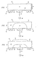
- FIG. 10 shows an implementation of a sensor device 100 in which an organic semiconductor layer 102 is mounted on a substrate 104 with a companion silicon chip 106 laterally spaced from the organic semiconductor layer 102.
- a support frame 108 is used to secure the peripheral edges of the organic semiconductor layer 102 to the substrate 104 and may include connection for the optional grounded surface grid discussed above with reference to FIGS. 4 and 5 .
- the substrate 104 includes an interconnect circuit (not shown) for interconnecting the organic semiconductor layer 102 with the companion silicon chip 106, and with contacts 110 at the periphery of the substrate 104 for communicating I/O signals with a system processor (not shown).
- Such interconnection techniques are well known in the packaging and PC board arts.
- the companion silicon chip 106 performs the complex control functions and communicates with the organic semiconductor layer 102, which includes an array of sensor cells, such as the 256-by-256 cell array of FIG. 7 .
- the structure of FIG. 10 may be packaged in a protective housing (not shown), which protects the silicon chip 106 from damage while leaving the upper surface of the organic semiconductor layer 102 exposed to perform its sensing function.
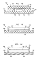
- FIGS. 11 through 15 show a sequence of steps for making a sensor device having an array of sensor cells formed in an organic semiconductor layer as previously described.
- a disposable, flexible polymer substrate 120 is provided with a peelable upper surface film 122.
- an organic semiconductor layer 124 is formed atop the peelable film 122, the layer 124 having a major surface contacting the peelable film and an exposed major surface opposite the peelable film.
- the layer 124 is preferably 20 to 25 microns thick.
- the peelable film 122 adheres more strongly to the disposable substrate 120 than to the organic semiconductor layer 124.
- a pattern of metal conductors 126 is created atop the organic semiconductor layer 124.
- a permanent substrate 128 with interconnect circuitry including upper surface contacts 130 for contacting the organic semiconductor layer conductors 126, and metal interconnect lines 132 that may be used to interconnect with a companion silicon chip or an external system processor (not shown).
- the structure of FIG. 13 has been inverted and mounted on the permanent substrate 128 so that conductors of the metal pattern 126 of the organic semiconductor layer 124 are contacted by the contacts 130 on the upper surface of the permanent substrate 128.
- FIG. 15 after the structure of FIG.
- the disposable substrate 120 with the peelable film 122 adhered thereto is peeled off of the organic semiconductor layer 124 to expose its sensing surface 134.
- the structure is then encapsulated or packaged to form the finished sensor device, leaving the sensing surface 134 exposed.
- FIG. 16 shows a device 140 in an alternative arrangement of the device 100 of FIG. 10 in which the silicon chip is housed beneath the organic semiconductor layer.
- an organic semiconductor layer 142 is mounted on an upper substrate 144, which in turn is mounted on an annular support 146 that includes an interior cavity that contains a companion silicon chip 148.
- These elements are mounted on a lower substrate 150, such as a PC board.
- the upper and lower substrates 144 and 150 include conventional interconnect circuitry (not shown).
- Conductors 152 may be arranged along the interior sidewalls of the annular support 146 to interconnect the upper substrate 144 with the lower substrate 150. Communications with a system processor (not shown) can be made through contacts 154 at the periphery of the lower substrate 150.
- the companion silicon chip 148 of the embodiment of FIG. 16 can include all of the addressing, control and sensing circuitry for communicating signals to and from the sensor array that is provided in the organic semiconductor layer 142.
- the column select circuitry, row select circuitry, load elements, input pulse generator, and control unit shown in FIG. 7 can be included in the silicon chip in either embodiment of FIGS. 10 or 16 : This simplifies the manufacturing process for making the organic semiconductor layer, which is much larger in area than the area needed for a companion silicon chip that is capable of performing the above-described functions.
- the use of a small silicon chip as a companion chip with a relatively large organic semiconductor layer that contains the sensor array achieves significant cost savings.
- the organic semiconductor layer is more durable than the relatively fragile silicon chips used in prior-art fingerprint detectors. It will be appreciated that the devices of FIGS. 10 and 16 can be repaired by replacing the organic semiconductor layers 102 and 142 in the event that they become damaged, salvaging the more expensive companion silicon chips for continued use.
- FIG. 17 shows a further alternative embodiment of the present invention in which the sensor device is generally designated by numeral 160.
- the sensor device is generally designated by numeral 160.
- two organic semiconductor layers 162 and 164 are included with one mounted atop the other to provide electrical communication therebetween.
- a sensor cell array as previously described is provided in the upper layer 162.
- Mounted immediately beneath the upper layer is the lower layer 164 that embodies all of the timing, control, sensing and processor logic of the previously described companion silicon chip.
- the fabrication of a more complex organic semiconductor layer is required for the embodiment of FIG. 17 and requires advanced processing techniques in which regions of both negative (n-type) and positive (p-type) charge carriers can be selectively formed in the organic semiconductor layer 164.
- metal interconnect conductors may be provided on the lower surface of the upper layer 162 and on both the upper and lower surfaces of the lower layer 164.
- the metal interconnect conductors of the lower layer 164 can be interconnected with contacts on the surface of a substrate 166, which also provides system I/O contacts 168 at its periphery.
- a frame 170 secures the organic semiconductor layers 162 and 164 to the substrate 166.
- FIG. 18 shows a further alternative embodiment 180 of the invention in which the embodiment 160 of FIG. 17 has been modified to include a reactive interface layer 182 on the upper surface of an upper organic semiconductor layer 184.
- a plurality of sensors such as the sixteen-cell sensor array of FIG. 6
- a control unit and select transistors similar to that as shown in FIG. 6 .
- a single sensor cell can be provided in the upper layer 184.
- the control unit and related functions for interacting with the sensor cell or sensor array in layer 184 can be provided in a lower organic semiconductor layer 186.
- Conductors on the bottom of the lower organic semiconductor layer 186 communicate with contacts on a substrate 188.
- the reactive interface layer 182 has an upper surface 190 that can be exposed to a test medium (gas or liquid) in contact therewith.
- the substrate 188 communicates with an external system processor (not shown) through contacts 192 at the periphery of the substrate 188.
- the reactive interface layer 182 comprises a polymer that may include a plurality of regions, each region located above a corresponding sensor cell in an array in the upper organic semiconductor layer 184.
- Each region in the reactive interface layer 182 includes a specific chemical that is contained within the polymer of the layer 182, the specific chemical being selectively reactive to a substance in the test medium contacting the upper surface 190 of the reactive interface layer 182.
- different enzymes can be provided in selected regions of the reactive interface layer 182. In operation, each enzyme catalyzes a reaction with a specific substance in the test medium. When this reaction occurs, a change in the charge potential at the isolated region of the reactive interface layer 182 occurs, which can be capacitively sensed by the sensor cell immediately below that particular region of the reactive interface layer. In this manner, the presence of various particular substances can be detected in the test medium.
- a single enzyme such as glucose oxidase
- a single enzyme can be provided in the reactive interface layer 182.
- a specific substance such as glucose
- a change in charge in the reactive interface layer is sensed by the sensor cell.
- a useful biochemical sensor device such as a blood glucose sensor, that can be disposed of after a single test procedure.
Landscapes
- Engineering & Computer Science (AREA)
- Physics & Mathematics (AREA)
- Health & Medical Sciences (AREA)
- General Physics & Mathematics (AREA)
- Life Sciences & Earth Sciences (AREA)
- Chemical & Material Sciences (AREA)
- Molecular Biology (AREA)
- Microelectronics & Electronic Packaging (AREA)
- Biochemistry (AREA)
- Pathology (AREA)
- Power Engineering (AREA)
- Immunology (AREA)
- Chemical Kinetics & Catalysis (AREA)
- Electrochemistry (AREA)
- Analytical Chemistry (AREA)
- General Health & Medical Sciences (AREA)
- Human Computer Interaction (AREA)
- Multimedia (AREA)
- Computer Hardware Design (AREA)
- Theoretical Computer Science (AREA)
- Spectroscopy & Molecular Physics (AREA)
- Measurement Of Length, Angles, Or The Like Using Electric Or Magnetic Means (AREA)
- Image Input (AREA)
Claims (20)
- Sensor (10), der Folgendes umfasst:eine organische Halbleiterschicht (12) mit einer oberen Fläche (18), die eine Erfassungsfläche definiert, und einer unteren Fläche (20), wobei die Schicht (12) ein Material mit beweglichen Majoritätsladungsträgern eines ersten Leitfähigkeitstyps umfasst, das überall in einer Zone unter der Erfassungsfläche verteilt ist;eine erste leitfähige Platte (P1), die von der Erfassungsfläche (18) beabstandet ist;eine zweite leitfähige Platte (P2), die von der Erfassungsfläche (18) und von der ersten leitfähigen Platte beabstandet ist; undeine Gate-Elektrode (G), wobei die Gate-Elektrode eine Raumladungszone (30) in die organische Halbleiterschicht unter der Erfassungsfläche als Reaktion auf eine Vorspannung, die an die Gate-Elektrode angelegt wird, einführen kann, wobei der Sensor dadurch gekennzeichnet ist, dass die Gate-Elektrode zwischen der ersten und der zweiten leitfähigen Platte eingeschoben ist und eine Abmessung der Raumladungszone sich als Reaktion auf das Vorliegen eines Objekts in der Nähe der Erfassungsfläche ändert, wobei das Ausmaß der Änderung der Abmessung erkannt werden kann, indem ein Signal erfasst wird, das von der ersten leitfähigen Platte durch die organische Halbleiterschicht (12) unter der Erfassungsfläche (18) an die zweite leitfähige Platte übermittelt wird, und wobei die erste leitfähige Platte (P1), die zweite leitfähige Platte (P2) und die Gate-Elektrode (G) an einer unteren Fläche (20) der organischen Halbleiterschicht (12) angebracht sind.
- Sensor (10) nach Anspruch 1, wobei der erste Leitfähigkeitstyp der p-Typ mit einer gleichmäßigen Verteilung von positiven beweglichen Majoritätsladungsträgern in einem Zustand ohne Vorspannung ist.
- Sensor (10) nach Anspruch 1, wobei die organische Halbleiterschicht (12) eine ungleichmäßige Verteilung des Materials mit p-Typ-Leitfähigkeit hat, wobei die Schicht einen verhältnismäßig dicken oberen Teil mit einer schwachen Konzentration des p-Typ-Materials, der sich von der Erfassungsfläche nach unten erstreckt, und einen verhältnismäßig dünnen unteren Teil (16) mit einer starken Konzentration des p-Typ-Materials aufweist, der sich von dem verhältnismäßig dicken oberen Teil nach unten zu der unteren Fläche (20) der Schicht entgegengesetzt zu der Erfassungsfläche erstreckt.
- Organisches Halbleitersensorbauelement (40), das Folgendes umfasst:eine organische Halbleiterschicht (42) mit einer oberen Fläche (44), die eine Erfassungsfläche definiert, und einer unteren Fläche (46), wobei die Schicht (42) ein Material mit beweglichen Majoritätsladungsträgern eines ersten Leitfähigkeitstyps umfasst, das überall in einer Zone unter der Erfassungsfläche verteilt ist; wobei die obere und die untere Fläche eben sind und in parallelen Ebenen voneinander beabstandet sind, wodurch die Dicke der Schicht definiert wird, und das Bauelement durch Folgendes gekennzeichnet ist:ein Muster von Leitern auf der unteren Fläche (46), das ein Array von Sensorzellen definiert, die in Zeilen und Spalten angeordnet sind, wobei die Leiter an jeder Zellenposition eine erste und eine zweite leitfähige Platte und eine Gate-Elektrode aufweisen, die zwischen den Platten eingeschoben ist;wobei die Gate-Elektrode jeder Zelle eine Raumladungszone in die organische Halbleiterschicht unter der Erfassungsfläche (44) als Reaktion auf eine Vorspannung, die an alle Gate-Elektroden einer ausgewählten Spalte angelegt wird, einführen kann, wobei die Raumladungszone sich von der unteren Fläche (46) nach oben erstreckt, wobei eine Abmessung der Raumladungszone in der Richtung senkrecht zu den parallelen Ebenen sich als Reaktion auf das Vorliegen eines Objekts in der Nähe der oberen Fläche ändert, wobei das Ausmaß der Änderung der Abmessung erkannt werden kann, indem ein Signal erfasst wird, das von der ersten leitfähigen Platte durch die organische Halbleiterschicht (42) unter der oberen Fläche (44) der Schicht an die zweite leitfähige Platte einer Zelle übermittelt wird, wobei das Signal durch die Zellen einer ausgewählten Zeile übermittelt wird, wobei nur eine Zelle des Arrays der ausgewählten Spalte und der ausgewählten Zeile entspricht, die jeweils erfasst werden; undwobei die ersten leitfähigen Platten, die zweiten leitfähigen Platten und die Gate-Elektroden an der unteren Fläche (46) der organischen Halbleiterschicht (42) angebracht sind.
- Organisches Halbleitersensorbauelement (40) nach Anspruch 4, wobei die organische Halbleiterschicht (42) ein Material mit p-Typ-Leitfähigkeit mit einer gleichmäßigen Verteilung von positiven beweglichen Majoritätsladungsträgern über den Platten jeder Sensorzelle umfasst, wenn die Schicht in einem Zustand ohne Vorspannung ist.
- Organisches Halbleitersensorbauelement (40) nach Anspruch 4 oder 5, das weiterhin Folgendes umfasst:eine Steuereinheit (62);Spaltenauswahlschaltkreise (76), die als Reaktion auf die Steuereinheit (62) zum Verbinden nur der Zellen der ausgewählten Spalte mit einer Spannungsquelle arbeiten, um Raumladungszonen über den Gates der Zellen der ausgewählten Spalte einzuführen; undZeilenauswahlschaltkreise (78), die als Reaktion auf die Steuereinheit (62) zum Verbinden nur der ausgewählten Zeile mit der Steuereinheit zum Erfassen des Signals, das durch die ausgewählte Zeile übermittelt wird, arbeiten.
- Organisches Halbleitersensorbauelement (40) nach Anspruch 6, das weiterhin Folgendes umfasst:einen Impulsgenerator, der mit den Zeilen verbunden ist, die unter der Steuerung der Steuereinheit (62, 72) arbeiten, zum Erzeugen des Signals, das durch die ausgewählte Zeile übermittelt wird; undein Lastelement (80) für jede Spalte, das die Spalte mit einem Masseanschluss verbindet, was bewirkt, dass die Gates der Zellen der nicht ausgewählten Spalten auf Masse entladen werden, während die Gates der Zellen der ausgewählten Spalte von der Spannungsquelle unter Spannung gesetzt werden.
- Organisches Halbleitersensorbauelement (40, 160) nach Anspruch 4, das Folgendes umfasst:ein Substrat (166) mit einer oberen Fläche mit Kontakten darauf;eine untere organische Halbleiterschicht (164), die auf die obere Fläche des Substrats (166) aufgebracht und damit elektrisch verbunden ist, wobei die untere organische Halbleiterschicht (164) Zonen mit n-Typ- und p-Typ-Leitfähigkeit darin aufweist, die Steuerschaltkreise definieren, wobei die organische Halbleiterschicht (162, 42) über der unteren organischen Halbleiterschicht (164) aufgebracht und damit elektrisch verbunden ist.
- Organisches Halbleitersensorbauelement (40, 160) nach Anspruch 8, wobei die organische Halbleiterschicht (42, 162) ein Material mit p-Typ-Leitfähigkeit überall in der organischen Halbleiterschicht hat.
- Organisches Halbleitersensorbauelement (40, 160) nach Anspruch 8 oder 9, wobei das Array von Sensorzellen dazu geeignet ist, das Vorliegen der Haut eines menschlichen Fingers in Kontakt mit der Erfassungsfläche (44) der organischen Halbleiterschicht zu erfassen, wobei die Sensorzellen dazu in der Lage sind, eine Fingerabdruckerhebung von einer Fingerabdruckvertiefung darauf unterscheiden können.
- Organisches Halbleitersensorbauelement (40, 160) nach Anspruch 8, 9 oder 10, wobei jede Sensorzelle dazu strukturiert ist, einen Sperrschicht-Feldeffekttransistor daselbst, den Transistor, bereitzustellen, wobei die Gate-Elektrode jeder Zelle selektiv mit Spannung versorgt werden kann, um zu bewirken, dass die Sensorzelle in einem Erfassungsmodus arbeitet, wenn die Gate-Elektrode mit Spannung versorgt wird, wobei jede Sensorzelle einen SFET-Kanal im Erfassungsmodus hat, wobei der SFET-Kanal eine elektrische Kapazität hat, die sich mit dem Vorliegen oder dem Fehlen eines Objekts in der Nähe der oberen Fläche (44) der oberen organischen Halbleiterschicht (42, 162) direkt über jeder Sensorzelle verändert.
- Organisches Halbleitersensorbauelement (40, 180) nach Anspruch 4, das weiterhin Folgendes umfasst:ein Substrat (188) mit einer oberen Fläche mit Kontakten darauf, wobei die organische Halbleiterschicht (42, 184) über dem Substrat getragen wird;eine reaktive Grenzflächenschicht (182), die auf der organischen Halbleiterschicht (42, 184) angeordnet ist, wobei die reaktive Grenzflächenschicht (182) eine freiliegende obere Fläche (190) hat, wobei die reaktive Grenzflächenschicht (190) ein Polymer umfasst, das eine Chemikalie enthält, die selektiv mit einer spezifischen Substanz in Kontakt mit der freiliegenden oberen Fläche (190) reaktiv ist;wobei eine Reaktion in der reaktiven Grenzflächenschicht (182) der Chemikalie darin mit der spezifischen Substanz von der Sensorzelle in der organischen Halbleiterschicht (42, 184) erfasst wird, wodurch das organische Halbleiterbauelement (40, 180) eine Aussetzung gegenüber der spezifischen Substanz erkennen kann.
- Organisches Halbleitersensorbauelement (180) nach Anspruch 12, wobei die Chemikalie ein Enzym ist.
- Organisches Halbleitersensorbauelement (180) nach Anspruch 13, wobei das Enzym Glukoseoxidase ist und die spezifische Substanz Glukose ist.
- Fingerabdruckdetektor, der Folgendes umfasst:das organische Halbleitersensorbauelement (40) nach Anspruch 4;ein Substrat (104), auf dem das organische Halbleiterbauelement (40) aufgebracht ist, wobei das Substrat (104) eine obere Fläche mit Kontakten darauf hat; undeinen Silizium-Halbleiterchip (106), der in der Nähe des organischen Halbleiterbauelements und in elektrischer Verbindung damit getragen wird;wobei ausgewählte Kontakte auf der oberen Fläche des Substrats (104) mit den Leitern auf der unteren Fläche des organischen Halbleiterbauelements verbunden sind.
- Fingerabdruckdetektor nach Anspruch 15, wobei das organische Halbleiterbauelement ein geerdetes Gitter aufweist, das darin an der Erfassungsfläche angeordnet ist.
- Fingerabdruckdetektor nach Anspruch 16, der weiterhin einen Rahmen (108) an den Umfangskanten des organischen Halbleiterbauelements zum Anbringen der Schicht an dem Substrat und Bereitstellen einer Verbindung zu dem Gitter umfasst.
- Fingerabdruckdetektor nach Anspruch 15, 16 oder 17, wobei der Silizium-Halbleiterchip (106) auf der oberen Fläche des Substrats (104) aufgebracht ist.
- Fingerabdruckdetektor nach einem der Ansprüche 15 bis 18, der weiterhin Folgendes umfasst:ein zweites Substrat (150), das unter dem Substrat (144) angeordnet ist, auf dem das organische Halbleiterbauelement aufgebracht ist; undeinen ringförmigen Träger (146), der auf dem zweiten Substrat (150) aufgebracht ist und die zwei Substrate aneinander anbringt, wobei der ringförmige Träger (146) eine innere Aussparung hat, die den Silizium-Halbleiterchip (148) enthält, wobei der Silizium-Halbleiterchip (148) auf dem zweiten Substrat (150) unter dem organischen Halbleiterbauelement aufgebracht ist.
- Verfahren zur Herstellung eines Sensorbauelements, wobei das Verfahren Folgendes umfasst:Bereitstellen eines flexiblen Polymersubstrats (120);Bilden eines abziehbaren Films (122) auf einer oberen Fläche des flexiblen Polymersubstrats (120);Bilden einer organischen Halbleiterschicht (124) auf dem abziehbaren Film (122), wobei die Schicht eine freiliegende Hauptfläche entgegengesetzt dem abziehbaren Film hat;wobei die organische Halbleiterschicht (124) eine obere ebene Fläche hat, die eine Erfassungsfläche definiert, und wobei die freiliegende Hauptfläche eine untere ebene Fläche ist, wobei die obere und die untere ebene Fläche in parallelen Ebenen voneinander beabstandet sind, wodurch die Dicke der Schicht definiert wird, wobei die Schicht ein Material mit beweglichen Majoritätsladungsträgern eines ersten Leitfähigkeitstyps umfasst, das überall in einer Zone unter der Erfassungsfläche verteilt ist;Erzeugen eines Musters von Leitern (126) auf der unteren ebenen Fläche der organischen Halbleiterschicht (124), wobei das Muster von Leitern ein Array von Sensorzellen definiert, die in Zeilen und Spalten angeordnet sind, wobei die Leiter an jeder Zellenposition eine erste und eine zweite leitfähige Platte und eine Gate-Elektrode aufweisen, die zwischen den Platten eingeschoben ist, wobei die ersten leitfähigen Platten, die zweiten leitfähigen Platten und die Gate-Elektroden an der unteren ebenen Fläche der Schicht angebracht sind;Bereitstellen eines permanenten Substrats (128) mit Kontakten (130) auf einer oberen Fläche dieses;Aufbringen der organischen Halbleiterschicht (124) mit dem flexiblen Polymersubstrat (120), das daran durch den abziehbaren Film (122) angebracht ist, auf dem permanenten Substrat (128) derart ausgerichtet, dass ausgewählte Leiter (126) des Musters von Leitern auf der organischen Halbleiterschicht mit den Kontakten (130) auf der oberen Fläche des permanenten Substrats in Kontakt kommen; undEntfernen des flexiblen Polymersubstrats (120) mit dem abziehbaren Film (122), der daran haftet, von der organischen Halbleiterschicht (124);wobei die Gate-Elektrode jeder Zelle eine Raumladungszone in die organische Halbleiterschicht unter der Erfassungsfläche als Reaktion auf eine Vorspannung, die an alle Gate-Elektroden einer ausgewählten Spalte angelegt wird, einführen kann, wobei die Raumladungszone sich von der unteren ebenen Fläche nach oben erstreckt, wobei eine Abmessung der Raumladungszone in der Richtung senkrecht zu den parallelen Ebenen sich als Reaktion auf das Vorliegen eines Objekts in der Nähe der oberen Fläche ändert, wobei das Ausmaß der Änderung der Abmessung erkannt werden kann, indem ein Signal erfasst wird, das von der ersten leitfähigen Platte durch die organische Halbleiterschicht unter der oberen Fläche der Schicht an die zweite leitfähige Platte einer Zelle übermittelt wird, wobei das Signal durch die Zellen einer ausgewählten Zeile übermittelt wird, wobei nur eine Zelle des Arrays der ausgewählten Spalte und der ausgewählten Zeile entspricht, die jeweils erfasst werden.
Applications Claiming Priority (2)
| Application Number | Priority Date | Filing Date | Title |
|---|---|---|---|
| US254311 | 2002-09-25 | ||
| US10/254,311 US6852996B2 (en) | 2002-09-25 | 2002-09-25 | Organic semiconductor sensor device |
Publications (3)
| Publication Number | Publication Date |
|---|---|
| EP1411552A2 EP1411552A2 (de) | 2004-04-21 |
| EP1411552A3 EP1411552A3 (de) | 2008-07-02 |
| EP1411552B1 true EP1411552B1 (de) | 2014-04-16 |
Family
ID=31993329
Family Applications (1)
| Application Number | Title | Priority Date | Filing Date |
|---|---|---|---|
| EP03255931.2A Expired - Lifetime EP1411552B1 (de) | 2002-09-25 | 2003-09-23 | Organischer Halbleitersensor |
Country Status (3)
| Country | Link |
|---|---|
| US (3) | US6852996B2 (de) |
| EP (1) | EP1411552B1 (de) |
| JP (1) | JP4426806B2 (de) |
Families Citing this family (37)
| Publication number | Priority date | Publication date | Assignee | Title |
|---|---|---|---|---|
| US7105462B2 (en) * | 2003-07-22 | 2006-09-12 | E. I. Du Pont De Nemours And Company | Lamination of organic semiconductor |
| KR100564915B1 (ko) * | 2004-02-10 | 2006-03-30 | 한국과학기술원 | 정전용량방식 지문센서 및 이를 이용한 지문 센싱방법 |
| US20070281362A1 (en) * | 2004-03-03 | 2007-12-06 | Koninklijke Philips Electronics, N.V. | Detection of No With a Semi-Conducting Compound and a Sensor and Device to Detect No |
| US20070241325A1 (en) * | 2004-06-10 | 2007-10-18 | Yamanashi University | Schottky Gate Organic Field Effect Transistor and Fabrication Method of the Same |
| AT413897B (de) * | 2004-09-08 | 2006-07-15 | Nanoident Technologies Ag | Vorrichtung zum erfassen eines fingerabdruckes |
| AT413896B (de) * | 2004-09-08 | 2006-07-15 | Nanoident Technologies Ag | Vorrichtung zum erfassen eines fingerabdruckes |
| US7710371B2 (en) * | 2004-12-16 | 2010-05-04 | Xerox Corporation | Variable volume between flexible structure and support surface |
| US8059102B2 (en) * | 2006-06-13 | 2011-11-15 | N-Trig Ltd. | Fingertip touch recognition for a digitizer |
| JP5324440B2 (ja) | 2006-07-12 | 2013-10-23 | エヌ−トリグ リミテッド | デジタイザのためのホバリングおよびタッチ検出 |
| US8686964B2 (en) * | 2006-07-13 | 2014-04-01 | N-Trig Ltd. | User specific recognition of intended user interaction with a digitizer |
| US20080121045A1 (en) * | 2006-11-29 | 2008-05-29 | Cole Matthew C | Multiplexed sensor array |
| US8542211B2 (en) * | 2007-01-03 | 2013-09-24 | Apple Inc. | Projection scan multi-touch sensor array |
| US8093689B2 (en) * | 2007-07-02 | 2012-01-10 | Infineon Technologies Ag | Attachment member for semiconductor sensor device |
| WO2010046904A2 (en) * | 2008-09-11 | 2010-04-29 | Indian Institute Of Technology Bombay | Method and device for determining ionizing radiation |
| JP2010122015A (ja) * | 2008-11-18 | 2010-06-03 | Fujitsu Ltd | センサユニット及び電子装置の製造方法 |
| CN101509888B (zh) * | 2009-03-20 | 2012-06-13 | 华东师范大学 | 硅基可集成微型葡萄糖传感器的制作方法 |
| US9494419B2 (en) * | 2009-07-31 | 2016-11-15 | Hewlett Packard Enterprise Development Lp | Beam direction sensor |
| TWI407561B (zh) * | 2009-11-10 | 2013-09-01 | Univ Nat Chiao Tung | 一種壓力感測元件及其陣列 |
| US9466382B2 (en) | 2012-11-14 | 2016-10-11 | Sandisk Technologies Llc | Compensation for sub-block erase |
| US8830717B2 (en) | 2012-11-29 | 2014-09-09 | Sandisk Technologies Inc. | Optimized configurable NAND parameters |
| US8988941B2 (en) | 2012-12-18 | 2015-03-24 | SanDisk Tehcnologies Inc. | Select transistor tuning |
| US9218890B2 (en) | 2013-06-03 | 2015-12-22 | Sandisk Technologies Inc. | Adaptive operation of three dimensional memory |
| US9142324B2 (en) | 2013-09-03 | 2015-09-22 | Sandisk Technologies Inc. | Bad block reconfiguration in nonvolatile memory |
| US9218886B2 (en) | 2013-12-10 | 2015-12-22 | SanDisk Technologies, Inc. | String dependent parameter setup |
| CN106407954A (zh) * | 2014-01-28 | 2017-02-15 | 深圳市汇顶科技股份有限公司 | 一种指纹识别模组、指纹识别装置及具有其的移动终端 |
| US9401216B1 (en) | 2015-09-22 | 2016-07-26 | Sandisk Technologies Llc | Adaptive operation of 3D NAND memory |
| US9691473B2 (en) | 2015-09-22 | 2017-06-27 | Sandisk Technologies Llc | Adaptive operation of 3D memory |
| GB2546995A (en) * | 2016-02-03 | 2017-08-09 | Cambridge Display Tech Ltd | A sensor for detection of a target species |
| JP6801370B2 (ja) * | 2016-10-28 | 2020-12-16 | 富士通株式会社 | センサ装置 |
| CN106897712B (zh) * | 2017-03-13 | 2020-01-14 | Oppo广东移动通信有限公司 | 指纹模组、显示屏和移动终端 |
| CN109308433B (zh) * | 2017-07-27 | 2022-09-20 | 中芯国际集成电路制造(上海)有限公司 | 一种半导体指纹传感器及其制作方法、电子装置 |
| US10781519B2 (en) * | 2018-06-18 | 2020-09-22 | Tokyo Electron Limited | Method and apparatus for processing substrate |
| CN109374023B (zh) * | 2018-10-25 | 2021-11-02 | 北京机械设备研究所 | 一种柔性可拉伸式传感器的制备方法 |
| CN110781804B (zh) * | 2019-10-23 | 2023-06-02 | 业泓科技(成都)有限公司 | 光学式影像辨识装置的制作方法 |
| US12033420B2 (en) * | 2020-06-23 | 2024-07-09 | Samsung Display Co., Ltd. | Display device |
| WO2022051152A1 (en) * | 2020-09-03 | 2022-03-10 | The Regents Of The University Of California | Pressure sensor device with organic electrochemical transistors |
| GB2602973B (en) * | 2021-01-20 | 2023-10-18 | Hyve Dynamics Holdings Ltd | A deformable sensing layer and methods |
Family Cites Families (32)
| Publication number | Priority date | Publication date | Assignee | Title |
|---|---|---|---|---|
| US3831432A (en) * | 1972-09-05 | 1974-08-27 | Texas Instruments Inc | Environment monitoring device and system |
| US4222903A (en) * | 1978-05-04 | 1980-09-16 | University Patents, Inc. | P-Type electrically conducting doped polyacetylene film and method of preparing same |
| US4353056A (en) * | 1980-06-05 | 1982-10-05 | Siemens Corporation | Capacitive fingerprint sensor |
| US4444892A (en) * | 1980-10-20 | 1984-04-24 | Malmros Mark K | Analytical device having semiconductive organic polymeric element associated with analyte-binding substance |
| GB2096825A (en) * | 1981-04-09 | 1982-10-20 | Sibbald Alastair | Chemical sensitive semiconductor field effect transducer |
| JPS5812370A (ja) * | 1981-07-15 | 1983-01-24 | Hitachi Ltd | 高分子半導体素子 |
| US4550221A (en) * | 1983-10-07 | 1985-10-29 | Scott Mabusth | Touch sensitive control device |
| US4717673A (en) * | 1984-11-23 | 1988-01-05 | Massachusetts Institute Of Technology | Microelectrochemical devices |
| JPS6283641A (ja) * | 1985-10-08 | 1987-04-17 | Sharp Corp | 電界効果型半導体センサ |
| US4894339A (en) * | 1985-12-18 | 1990-01-16 | Seitaikinouriyou Kagakuhin Sinseizogijutsu Kenkyu Kumiai | Immobilized enzyme membrane for a semiconductor sensor |
| JPS63131057A (ja) * | 1986-11-20 | 1988-06-03 | Terumo Corp | 酵素センサ |
| JP2609366B2 (ja) * | 1989-01-10 | 1997-05-14 | 三菱電機株式会社 | 電界効果型トランジスタ及びこれを用いた液晶表示装置 |
| GB9116360D0 (en) * | 1991-07-29 | 1991-09-11 | Neotronics Ltd | Device for sensing volatile materials |
| US6278127B1 (en) * | 1994-12-09 | 2001-08-21 | Agere Systems Guardian Corp. | Article comprising an organic thin film transistor adapted for biasing to form a N-type or a P-type transistor |
| US5719033A (en) * | 1995-06-28 | 1998-02-17 | Motorola, Inc. | Thin film transistor bio/chemical sensor |
| US5625199A (en) * | 1996-01-16 | 1997-04-29 | Lucent Technologies Inc. | Article comprising complementary circuit with inorganic n-channel and organic p-channel thin film transistors |
| US6326640B1 (en) * | 1996-01-29 | 2001-12-04 | Motorola, Inc. | Organic thin film transistor with enhanced carrier mobility |
| US5763943A (en) * | 1996-01-29 | 1998-06-09 | International Business Machines Corporation | Electronic modules with integral sensor arrays |
| US6114862A (en) * | 1996-02-14 | 2000-09-05 | Stmicroelectronics, Inc. | Capacitive distance sensor |
| GB9615605D0 (en) * | 1996-07-25 | 1996-09-04 | British Nuclear Fuels Plc | Polymer radiation sensors |
| GB9626217D0 (en) * | 1996-12-18 | 1997-02-05 | Aromascan Plc | Gas sensor |
| US5981970A (en) * | 1997-03-25 | 1999-11-09 | International Business Machines Corporation | Thin-film field-effect transistor with organic semiconductor requiring low operating voltages |
| KR100303934B1 (ko) * | 1997-03-25 | 2001-09-29 | 포만 제프리 엘 | 낮은작동전압을필요로하는유기반도체를갖는박막전장효과트랜지스터 |
| US6252245B1 (en) * | 1999-03-29 | 2001-06-26 | Howard Edan Katz | Device comprising n-channel semiconductor material |
| GB9922572D0 (en) * | 1999-09-24 | 1999-11-24 | Koninkl Philips Electronics Nv | Capacitive sensing array devices |
| US6344664B1 (en) | 1999-12-02 | 2002-02-05 | Tera Connect Inc. | Electro-optical transceiver system with controlled lateral leakage and method of making it |
| GB2370410A (en) * | 2000-12-22 | 2002-06-26 | Seiko Epson Corp | Thin film transistor sensor |
| US6575013B2 (en) * | 2001-02-26 | 2003-06-10 | Lucent Technologies Inc. | Electronic odor sensor |
| US6661299B2 (en) * | 2001-02-26 | 2003-12-09 | Lucent Technologies Inc. | Odor sensor with organic transistor circuitry |
| JP4087125B2 (ja) * | 2001-03-07 | 2008-05-21 | シャープ株式会社 | 凹凸パターン検出素子 |
| US6672174B2 (en) | 2001-07-23 | 2004-01-06 | Fidelica Microsystems, Inc. | Fingerprint image capture device with a passive sensor array |
| DE10211900A1 (de) * | 2002-03-18 | 2003-10-16 | Infineon Technologies Ag | Biosensor zum Erfassen von makromolekularen Biopolymeren und Verfahren zur Herstellung eines Biosensors zum Erfassen von makromolekularen Biopolymeren |
-
2002
- 2002-09-25 US US10/254,311 patent/US6852996B2/en not_active Expired - Lifetime
-
2003
- 2003-09-23 EP EP03255931.2A patent/EP1411552B1/de not_active Expired - Lifetime
- 2003-09-25 JP JP2003334020A patent/JP4426806B2/ja not_active Expired - Lifetime
-
2004
- 2004-12-22 US US11/021,063 patent/US7141839B2/en not_active Expired - Lifetime
-
2006
- 2006-10-13 US US11/580,582 patent/US8569809B2/en not_active Expired - Fee Related
Also Published As
| Publication number | Publication date |
|---|---|
| US20070029583A1 (en) | 2007-02-08 |
| US6852996B2 (en) | 2005-02-08 |
| US8569809B2 (en) | 2013-10-29 |
| US20050110055A1 (en) | 2005-05-26 |
| EP1411552A2 (de) | 2004-04-21 |
| JP2004125791A (ja) | 2004-04-22 |
| US20040056245A1 (en) | 2004-03-25 |
| JP4426806B2 (ja) | 2010-03-03 |
| US7141839B2 (en) | 2006-11-28 |
| EP1411552A3 (de) | 2008-07-02 |
Similar Documents
| Publication | Publication Date | Title |
|---|---|---|
| EP1411552B1 (de) | Organischer Halbleitersensor | |
| JP4169395B2 (ja) | ソリッドステート指紋センサーパッケージング装置及び方法 | |
| US8702921B2 (en) | Biosensors array and method for operating a biosensor array | |
| EP2589065B1 (de) | Chemisch empfindlicher sensor mit leicht dotierten abflüssen | |
| JP3969702B2 (ja) | センサ・セル、センサ、サンプルを同定する方法、化学センサ、指紋認識装置、バイオセンサの操作方法、及び指紋認識装置の操作方法 | |
| CA2259406C (en) | Multiplexed active biologic array | |
| US6111280A (en) | Gas-sensing semiconductor devices | |
| US6856161B2 (en) | Sensor array and method for detecting the condition of a transistor in a sensor array | |
| US4397714A (en) | System for measuring the concentration of chemical substances | |
| Milgrew et al. | The fabrication of scalable multi-sensor arrays using standard CMOS technology [chemical sensors] | |
| US20020114125A1 (en) | Capacitance type humidity sensor and manufacturing method of the same | |
| KR970003739A (ko) | 박막 트랜지스터를 이용한 생화학적 감지기 및 그 제조 방법 | |
| JP2021510196A (ja) | デジタルマイクロ流体デバイス、マイクロ流体装置、ラボオンチップデバイス、デジタルマイクロ流体方法、及びデジタルマイクロ流体デバイスの製造方法 | |
| CN115791908B (zh) | 一种基于1t1c结构的电化学传感器、电化学传感系统 | |
| US20160313282A1 (en) | Motft and array circuit for chemical/biochemical applications | |
| EP4191870A1 (de) | Sensorschwachsignalleseschaltung | |
| Fiaccabrino et al. | Array of individually addressable microelectrodes | |
| Al-Ahdal et al. | ISFET-based chemical switch | |
| CN115096965B (zh) | 薄膜晶体管型生化传感微阵列芯片及其制备方法 | |
| CN116635714B (zh) | 离子传感器及离子传感器的制造方法 | |
| CN118655204A (zh) | 气体传感器、传感器阵列及显示面板 | |
| JPH0682419A (ja) | ガスセンサ |
Legal Events
| Date | Code | Title | Description |
|---|---|---|---|
| PUAI | Public reference made under article 153(3) epc to a published international application that has entered the european phase |
Free format text: ORIGINAL CODE: 0009012 |
|
| AK | Designated contracting states |
Kind code of ref document: A2 Designated state(s): AT BE BG CH CY CZ DE DK EE ES FI FR GB GR HU IE IT LI LU MC NL PT RO SE SI SK TR |
|
| AX | Request for extension of the european patent |
Extension state: AL LT LV MK |
|
| RIC1 | Information provided on ipc code assigned before grant |
Ipc: G06K 9/00 20060101AFI20080229BHEP |
|
| PUAL | Search report despatched |
Free format text: ORIGINAL CODE: 0009013 |
|
| AK | Designated contracting states |
Kind code of ref document: A3 Designated state(s): AT BE BG CH CY CZ DE DK EE ES FI FR GB GR HU IE IT LI LU MC NL PT RO SE SI SK TR |
|
| AX | Request for extension of the european patent |
Extension state: AL LT LV MK |
|
| 17P | Request for examination filed |
Effective date: 20081222 |
|
| AKX | Designation fees paid |
Designated state(s): DE FR GB IT |
|
| 17Q | First examination report despatched |
Effective date: 20110428 |
|
| RAP1 | Party data changed (applicant data changed or rights of an application transferred) |
Owner name: STMICROELECTRONICS, INC. |
|
| REG | Reference to a national code |
Ref country code: DE Ref legal event code: R079 Ref document number: 60346009 Country of ref document: DE Free format text: PREVIOUS MAIN CLASS: G06K0009000000 Ipc: G01N0027327000 |
|
| RIC1 | Information provided on ipc code assigned before grant |
Ipc: G01L 1/14 20060101ALI20130710BHEP Ipc: G01N 27/414 20060101ALI20130710BHEP Ipc: G06K 9/00 20060101ALI20130710BHEP Ipc: H01L 27/30 20060101ALI20130710BHEP Ipc: H01L 51/05 20060101ALI20130710BHEP Ipc: G01N 27/327 20060101AFI20130710BHEP |
|
| GRAP | Despatch of communication of intention to grant a patent |
Free format text: ORIGINAL CODE: EPIDOSNIGR1 |
|
| INTG | Intention to grant announced |
Effective date: 20130926 |
|
| GRAS | Grant fee paid |
Free format text: ORIGINAL CODE: EPIDOSNIGR3 |
|
| GRAA | (expected) grant |
Free format text: ORIGINAL CODE: 0009210 |
|
| AK | Designated contracting states |
Kind code of ref document: B1 Designated state(s): DE FR GB IT |
|
| REG | Reference to a national code |
Ref country code: GB Ref legal event code: FG4D |
|
| REG | Reference to a national code |
Ref country code: DE Ref legal event code: R096 Ref document number: 60346009 Country of ref document: DE Effective date: 20140528 |
|
| REG | Reference to a national code |
Ref country code: DE Ref legal event code: R097 Ref document number: 60346009 Country of ref document: DE |
|
| PLBE | No opposition filed within time limit |
Free format text: ORIGINAL CODE: 0009261 |
|
| STAA | Information on the status of an ep patent application or granted ep patent |
Free format text: STATUS: NO OPPOSITION FILED WITHIN TIME LIMIT |
|
| 26N | No opposition filed |
Effective date: 20150119 |
|
| PG25 | Lapsed in a contracting state [announced via postgrant information from national office to epo] |
Ref country code: IT Free format text: LAPSE BECAUSE OF FAILURE TO SUBMIT A TRANSLATION OF THE DESCRIPTION OR TO PAY THE FEE WITHIN THE PRESCRIBED TIME-LIMIT Effective date: 20140416 |
|
| REG | Reference to a national code |
Ref country code: DE Ref legal event code: R097 Ref document number: 60346009 Country of ref document: DE Effective date: 20150119 |
|
| GBPC | Gb: european patent ceased through non-payment of renewal fee |
Effective date: 20140923 |
|
| REG | Reference to a national code |
Ref country code: FR Ref legal event code: ST Effective date: 20150529 |
|
| PG25 | Lapsed in a contracting state [announced via postgrant information from national office to epo] |
Ref country code: GB Free format text: LAPSE BECAUSE OF NON-PAYMENT OF DUE FEES Effective date: 20140923 |
|
| PG25 | Lapsed in a contracting state [announced via postgrant information from national office to epo] |
Ref country code: FR Free format text: LAPSE BECAUSE OF NON-PAYMENT OF DUE FEES Effective date: 20140930 |
|
| REG | Reference to a national code |
Ref country code: DE Ref legal event code: R082 Ref document number: 60346009 Country of ref document: DE Representative=s name: PAGE, WHITE & FARRER GERMANY LLP, DE |
|
| PGFP | Annual fee paid to national office [announced via postgrant information from national office to epo] |
Ref country code: DE Payment date: 20220818 Year of fee payment: 20 |
|
| REG | Reference to a national code |
Ref country code: DE Ref legal event code: R071 Ref document number: 60346009 Country of ref document: DE |