EP1401105A1 - Procédé pour la compensation de tension de décalage pour convertisseurs analogiques-numériques parallèles à entrelacement temporel et circuit pour celui-ci - Google Patents
Procédé pour la compensation de tension de décalage pour convertisseurs analogiques-numériques parallèles à entrelacement temporel et circuit pour celui-ci Download PDFInfo
- Publication number
- EP1401105A1 EP1401105A1 EP02425563A EP02425563A EP1401105A1 EP 1401105 A1 EP1401105 A1 EP 1401105A1 EP 02425563 A EP02425563 A EP 02425563A EP 02425563 A EP02425563 A EP 02425563A EP 1401105 A1 EP1401105 A1 EP 1401105A1
- Authority
- EP
- European Patent Office
- Prior art keywords
- digital
- analog
- digital converter
- cod
- adc
- Prior art date
- Legal status (The legal status is an assumption and is not a legal conclusion. Google has not performed a legal analysis and makes no representation as to the accuracy of the status listed.)
- Granted
Links
Images


Classifications
-
- H—ELECTRICITY
- H03—ELECTRONIC CIRCUITRY
- H03M—CODING; DECODING; CODE CONVERSION IN GENERAL
- H03M3/00—Conversion of analogue values to or from differential modulation
- H03M3/30—Delta-sigma modulation
- H03M3/38—Calibration
- H03M3/382—Calibration at one point of the transfer characteristic, i.e. by adjusting a single reference value, e.g. bias or gain error
- H03M3/384—Offset correction
-
- H—ELECTRICITY
- H03—ELECTRONIC CIRCUITRY
- H03M—CODING; DECODING; CODE CONVERSION IN GENERAL
- H03M3/00—Conversion of analogue values to or from differential modulation
- H03M3/30—Delta-sigma modulation
- H03M3/458—Analogue/digital converters using delta-sigma modulation as an intermediate step
- H03M3/466—Multiplexed conversion systems
- H03M3/468—Interleaved, i.e. using multiple converters or converter parts for one channel, e.g. using Hadamard codes, pi-delta-sigma converters
- H03M3/47—Interleaved, i.e. using multiple converters or converter parts for one channel, e.g. using Hadamard codes, pi-delta-sigma converters using time-division multiplexing
Definitions
- the present invention relates to the conversion of electrical signals into the digital form, and more precisely to a voltage offset compensation method for time-interleaved multi-path analog-to-digital sigma-delta converters and a respective circuit.
- ADC Analog-to-Digital Converters
- BTSs wide-band Base Transceiver Stations
- SFDR Spurious Free Dynamic Range
- sigma-delta converters are able to feature a "band-pass" transfer function, centred at the desired IF. Such a solution allows to digitise the only band around IF, thus reducing the in-band thermal noise requirements and to optimise the quantization noise and the linearity in the only band of interest.
- OSR F CK /2BW required to obtain the desired Signal-to-Noise Ratio (SNR) with a given signal bandwidth BW, so that the higher is OSR the better is the SNR.
- SNR Signal-to-Noise Ratio
- a significant work in the field of sigma-delta converters is the following: [Ref.1] - S. Norsworthy, R. Schreirer, G. Temes, "Delta-Sigma Data Converters - Theory, Design and Simulation", IEEE Press, NJ, USA, 1997.
- Fig.2 shows a general block diagram of a band-pass sigma-delta converter (or ⁇ or delta-sigma).
- a sampling stage 1 for sampling the analog input signal Vin at a sampling frequency F CK
- an analog 2-input adder (subtractor) 2 for sampling the analog input signal Vin at a sampling frequency F CK
- an analog 2-input adder (subtractor) 2 for sampling the analog input signal Vin at a sampling frequency F CK
- an analog 2-input adder (subtractor) 2 for sampling the analog input signal Vin at a sampling frequency F CK
- an analog 2-input adder (subtractor) 2 for sampling the analog input signal Vin at a sampling frequency F CK
- an analog 2-input adder (subtractor) 2 for sampling the analog input signal Vin at a sampling frequency F CK
- an analog 2-input adder (subtractor) 2 for sampling the analog input signal Vin at a sampling frequency F CK
- an analog 2-input adder (subtractor) 2 for sampling the analog
- the sampling frequency F CK is higher than the Nyquist limit and the sigma-delta is an oversampling converter consequently.
- the analog filter 3 has a band-pass transfer function of the first order, suitably centred at the desired IF.
- the comparator 4 together with latch 5 constitutes a quantizer operating as 1-bit ADC.
- the switch 6 and the two thresholds +V R and V R constitute a feedback de-quantizer operating as 1-bit DAC. As it is well known, the same structure can be extended also to multi-bit solutions.
- the feedback structure of the sigma-delta converter makes it intrinsically less sensitive to component matching with respect to conventional ADC and allows the quantization noise, introduced by the comparator 4, to be shifted out of the signal band.
- This last effect called noise shaping, makes the Signal Transfer Function (STF) different from that of the quantization Noise Transfer Function (NTF); the filter 3 provides the necessary transfer function to obtain the desired STF and NTF functions.
- STF Signal Transfer Function
- NTF quantization Noise Transfer Function
- the combined effect of over-sampling and noise shaping enables to obtain high resolutions with reasonable clock frequencies.
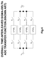
- Fig.3 illustrates in outline a time-interleaved ADC of the known art including an analog demultiplexer 7 operated at F CK clock for distributing the input signal V in in turn to M identical ADC 1 , ADC 2 , ...., ADC M converters.
- the outputs of ADC 1 toM converters are connected to respective inputs of a digital demultiplexer 8 operated at F CK clock which in turn forwards the ADC 1 to M output signals to the unique V out port, thus forming a high-speed digitally converted signal V out .
- the converters ADC 1 to M can be of any type and are operated at F CK /M where F CK is the total sampling frequency of the time-interleaved ADC and M is the number of channels (or paths). The speed requirements on each converter are relaxed by a factor M. Obviously, the number of converters is at the same time increased by the same factor, resulting in a large chip area and high power consumption.
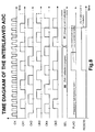
- Fig.4 shows an example of implementation of a time-interleaved ADC like the one of the preceding Fig.3 based on a 4-path band-pass sigma-delta ADC.
- the detail of the ADC of fig.4 is disclosed in the following [Ref.5]: A. Centuori, U. Gatti, P. Malcovati, F. Maloberti, "A 320-MHz Four-Paths Bandpass Sigma-Delta Modulator", Proc. IEEE Instrum. and Meas. Techn. Conference, Anchorage, AK, USA, pp. 497-500, incorporated by reference.
- each channel LP-SD 1 to 4 features a low-pass signal transfer function STF (and high-pass NTF) at a clock frequency F CK /4 of a respective timing signal ⁇ 1 to ⁇ 4 .
- T ck is the sampling period at the modulator output (not visible in the Figure)
- H P (z) has low-pass shape, its attenuation spectrum is replicated every F ck /4, as shown in fig.5 for the H TOT (f) frequency spectrum, thus leading to the desired band-pass signal transfer function around IF (and consequently notch transfer function for the quantization noise).
- the main advantage of this solution is that every channel operates at a frequency that is a quarter of the equivalent converter speed.
- the low-pass transfer function is inherently less sensitive to capacitance mismatches than the band-pass transfer function.
- the multi-path topology allows achieving the same SNR performance than single-path topologies with a higher-order filtering, with benefits in the stability and in the complexity design.
- any mismatch between the time-interleaved channels gives rise to degradation in the linearity performances.
- the mismatch of the voltage offset value in the different paths is the most critical one and is a priori unpredictable.
- the voltage offset mismatch can generate severe limitation in the maximum Spurious-Free Dynamic Range (SFDR) and SNR performance. For example a mismatch of 10 mV RMS of the offsets introduces a degradation of 60 dB in the converter SNR and SFDR parameters.
- the performance of the time-interleaved converter is of course limited by the accuracy of the ADCs in every path, but there are additional errors caused by mismatches between the channels.
- There are three main sources of error in the time-interleaved systems, phase skew errors, gain errors and voltage offset. The latter is the most critical one for the receiver application since it causes the raising of signal independent tones located at (F ck /M) ⁇ N (N 0, 1, ... M-1), exactly where the wanted input signal is present.
- This drawback is pointed out in the following [Ref.6]: M. Gustavsson, J. J. Wikner, N. N. Tan, "CMOS Data Converters for Communications", Kluwer Academic Publishers, Boston, USA, 2000).
- on-line calibration techniques are more difficult to implement, since they operate in background while the ADC is working normally.
- Several solutions for achieving on-line calibration has been presented before: they can be analog or digital. Usually it is preferred to operate in the digital domain, since the digital world it less prone to inaccuracy and digital data are easier to be processed.
- Unfortunately most popular on-line calibration techniques are only suitable for deterministic interleaved ADC and cannot be applied to sigma-delta modulators in view of their stochastic behaviour making the output signals obtained with the same input signal at different times each other different depending on the previous history.
- the main object of the present invention is that to overcome the above-mentioned limits in time-interleaved multi-path ADCs, in particular by providing an on-line digital calibration technique that allows to reduce the amplitude of the undesired tones caused by mismatches between the offsets of the different paths and that is easy to use in any type of analog-to-digital converters, especially sigma-delta.
- the subject of the present invention is a method for compensating the voltage offset of the various paths in a multi-path time-interleaved analog-to-digital converter exploiting an additional reference path cyclically connected in parallel to each of the M paths to be calibrated for calculating the differences between successive digital outputs of the two paths, and accumulating the differences over a given time slot, thus producing a digital word which is added to the output of the path under calibration, preventively multiplied by a scale factor which depends on the length of the given time slot, making the offset of each path depending on the offset of the only reference path, as disclosed in claim 1.
- object of the method invention is an embodiment in which the accumulation of the differences between successive digital outputs of the reference and the calibrating paths is completed with the average over the number of samples considered in the given time slot, and the multiplication by a scale factor is unnecessary, as disclosed in the independent claim 2.
- the two embodiments are substantially equivalent as far as concern the offset compensation, but hardware implementation of first embodiment is simpler because in the second as many digital divisions as the M paths are needed.
- the method of the invention allows continuously running background calibration since it does not affect the normal operation of the ADC under calibration. Moreover since the M paths are never disconnected from the input signal, no discontinuity is produced and this method can be applied to any kind of analog-to-digital converter, in particular time-interleaved sigma-delta ADC, to whom conventional calibration methods cannot be applied because of their stochastic behaviour.
- a preferred embodiment of the invention is a circuit that performs the operations foreseen by the on-line voltage offset compensation method, as disclosed in a relative independent claim.
- This digital circuit can be implemented with an external FPGA (Field Programmable Gate Arrays) or integrated on the same chip together with the time-interleaved ADC and occupies a moderate silicon area.
- the last solution constitutes a time-interleaved ADC having high operating frequency together with satisfactory SNR and SFDR, as required by recent BTS standards, without using particular manufacturing technologies.
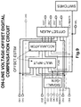
- Block ADC-BANK includes four Analog-to-Digital Converters ADC1 to ADC4 plus an additional reference ADC5 one.
- the A/D converters ADC1 to ADC5 can be of any type, in particular sigma-delta.
- Block OFFSET-ALIGN includes a SCALER, four two-input digital adders, and a DE-SCALER.
- the SIGNAL-GEN block receives a system clock CK and an external RESET and generates the following timing signals: CK1 to CK5, SEL, FLAG, and RESET5 directed to the other blocks as shown in the Figure to control their operation.
- the analog input signal V in which has to be digitally converted reaches the input of the analog demultiplexer ANALOG-DEMUX, whose four outputs are connected to the input of the four converters ADC1 to ADC4 inside the ADC-BANK and to the four inputs of the analog block SWITCHES.
- At the outputs of the converters ADC1 to ADC4 are in turn present four digital signals CH1 to CH4 directed to the inputs (-) of the digital OFFSET-ESTIM block.
- the unique output of the analog block SWITCHES is connected to the input of the fifth ADC5 converter whose digital output signal CH5 reaches the input (+) of the OFFSET-ESTIM block.
- the four outputs of the last block are connected to first inputs of four respective two-inputs digital adders included in the OFFSET-ALIGN block, while second inputs of the adders are connected to the outputs of the block SCALER which receives the CH1 to CH4 signals from the outputs of the ADC-BANK.
- the outputs of the four digital adders are connected to the inputs of the block DE-SCALER, whose outputs are connected to the inputs of the digital multiplexer DIGITAL-MUX that outputs the high-speed digitally converted signal V out .
- Both ANALOG-DEMUX and DIGITAL-MUX are controlled by means of the CK clock.
- the block SIGNAL-GEN is implemented by means of a Finite-State-Machine (FSM) that generates the timing waveshapes visible in fig.8 .
- FSM Finite-State-Machine
- the analog demultiplexer ANALOG-DEMUX distributes with frequency F CK the analog input signal V in in turn to the ADC1 to ADC4 converters for the normal time-interleaved A/D conversion.
- the analog block SWITCHES is controlled by signal SEL to connect the one of the ADC1 to 4 converters to be calibrated in parallel to the additional ADC5 converter.
- the four outputs of the OFFSET-ESTIM block are all zero and at the four outputs of the OFFSET-ALIGN block there are the four uncalibrated time-interleaved digitally converted signals; these signals are multiplexed by DIGITAL-MUX block with frequency F CK to constitute the overall high-speed digitally converted signal V out .
- the calibration procedure is started by the reset signal RESET5 directed to the ADC5 reference ADC.
- the reference path operates with a proper clock CK5 at a frequency F CK /M, which is phase aligned to the clock signal of the path to be calibrated, as shown in fig.8.
- Block OFFSET-ALIGN adds up this word to the ADC output of the path under calibration opportunely multiplied by a scale factor which depends on the length of the given time slot, thus making the offset of the path under calibration dependent on the offset of the only reference path ADC5, as will be better described with reference to fig.10a.
- the words at the output of the relevant digital adder inside the block OFFSET-ALIGN are de-scaled by the same scale factor restoring the original converted value in which the contribute of the original voltage offset is replaced with the voltage offset of the reference path, as will be better described with reference to fig.10b.
- the procedure is indefinitely repeated for the M paths ADC1 to ADC4 of the ADC-BANK selected by a modulo-2 counting of the two bits SEL signal. After a reasonably time the voltage offset of each of the M paths is the same and is equally dependent on the offset of the reference path ADC5 (not necessarily zero), thus the high-speed digital signal V out can benefit of the advantages of calibration.
- the offset of the reference path ADC5 can be periodically calibrated in order to make the offsets of all the paths equal to zero.
- the SNR degradation in time-interleaved ADC is directly proportional to the variance ⁇ off of the offset mismatch.
- the duration of time slot TS influences the precision with which the offset correction is performed: the higher is TS the better is the SNR obtained with the same offset mismatch between the two paths. If the variance ⁇ off increases the time slot TS has to be increased. Depending on the variance ⁇ off and on the required offset compensation, an optimum value for TS and for the number of bit in the digital offset estimation is determined. In principle, the offset to be compensated can be allowed to be large without effect on the SNR of the output signal V out .
- the input signal V in can have any frequency components, including those located around F CK /M, thus overcoming the limits of the method reported in [REF.12].
- the calibration signal does not interfere with the wanted signal the full-scale range of the various ADCs is available for the input signal.
- the proposed calibration technique is purely digital, it does not operate on any analog section of the ADCs and is essentially applied at the output. Therefore, it is intrinsically robust and does not exhibit the critical issues of the method reported in [REF.15] .
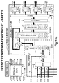
- FIG.9 a block diagram of the only voltage offset compensation circuit belonging to the multi-path ADC of the previous fig.7 is shown. Elements and signals equal in the two Figures are equally labelled.
- the voltage offset compensation circuit visible in the previous fig.7 included the following blocks: SWITCHES, OFFSET-ESTIM, and OFFSET-ALIGN; block SIGNAL-GEN reasonably belongs both to the multi-path ADC for the generation of CK1 to CK4 clocks (which time the normal operation even without compensation) and to the compensation circuit for the generation of the remaining timing signals: SEL, CK5, RESET5, and FLAG.
- the compensation circuit of fig.9 is more detailed than the one coarsely indicated in fig.7 and two new blocks MULT-INPUT and ACCUMULATOR replace the previous blocks OFFSET-ESTIM.
- Block MULT-INPUT receives the signal CH1 to CH4 from the ADC1 to 4 to be calibrated and signal CH5 from the reference ADC5.
- the digital output of block MULT-INPUT is connected to the input of the cascaded block ACCUMULATOR for delivering the calculated differences.
- Block ACCUMULATOR receives the difference values and integrates them over a given time slot TS, obtaining integration data forwarded to the four inputs of the cascaded block OFFSET-ALIGN.
- This last block compensates the estimated voltage offset of the four CH1 to 4 digital signals, as already said, and outputs four compensated words CH1", CH2", CH3", and CH4" directed to the cascaded block DIGITAL-MUX belonging to the multi-path ADC (fig.7).
- An external signal RESET is directed to all the blocks visible in fig.9 (SIGNAL-GEN included) for the correct initialisation of the operation.
- the timing signals SEL, RESET5 and CK5 are addressed both to the MULT-INPUT and ACCUMULATOR blocks, while FLAG is directed to the only ACCUMULATOR block.
- block SWITCHES implements the connection of the additional reference ADC5 in parallel to the one of the ADC1 to 4 converters to be calibrated selected by signal SEL.
- Block MULT-INPUT performs the difference between the outputs of these two paths and delivers it to the block ACCUMULATOR.
- Block ACCUMULATOR receives the differences between the output signal of the reference path ADC5 and of the path under calibration and integrates them over a given time slot TS.
- Signal FLAG directed to the block ACCUMULATOR detects when the averaging phase is terminated and the result can be delivered to an internal output buffer (not visible in fig.8).
- signal SEL performs the multiplexing of the outputs, which are the offset estimation of the four interleaved ADCs, to the proper channel.
- Figures 10a and 10b show with greater detail the device of the preceding fig.9 in order to point out the internal structure of the various registers and the dimension of the relevant buses.
- the block MULT-INPUT is implemented by means of a digital multiplexer MUX 9 driven by the 2-bit SEL signal, which sequentially selects one of the N-bit (including the sign) digital signals CH1 to 4 of the paths to be calibrated.
- MUX 9 driven by the 2-bit SEL signal, which sequentially selects one of the N-bit (including the sign) digital signals CH1 to 4 of the paths to be calibrated.
- it includes a subtractor 10 that calculates the algebraic difference between the N-bit reference signal CH5 and the selected signal.
- a register K-BIT-REG 11 transforms the word at the output of the subtractor 10 into a K-bit word (K > N) to be sent to the block ACCUMULATOR.
- the block ACCUMULATOR includes the following blocks: a digital adder 12, a register K-BIT-ACCUMULATOR 13, a buffer register K-BIT-BUFFER 14, a three state buffer THREE-STATE 15, a digital demultiplexer DEMUX 16, and four K-bit registers 17, 18, 19, and 20.
- the output of block 13 is fed into the K-BIT-BUFFER 14, which is isolated from the input of demultiplexer DEMUX 16 by the THREE-STATE interface 15 placed in-between.
- Three-state 15 is put in high impedance state when the accumulator 13 is working.
- the assertion of the signal FLAG enable the three-state to forward the result of the offset accumulation to the input of the demultiplexer DEMUX 16 which transfers it, depending on the signal SEL, to the proper output connected to one of the four K-bit registers 17 to 20. While circuits preceding the demultiplexer DEMUX 16 is shared among the various channels CH1 to CH4, the successive circuits are dedicated; these last include registers 17 to 20, whose K-bit outputs are indicated with DH1, DH2, DH3, and DH4. The value in turn stored in the selected register at the output of DEMUX 16 remains stable until the next value is overwritten (at the begin of TS+4 integration time slot) to allow voltage offset compensation with an updated offset value.
- the OFFSET-ALIGN block includes: the block SCALER, in its turn comprising four registers K-BIT-REG 21 to 24, four digital adders 25 to 28, and the block DE-SCALER 29.
- the N-bit signals CH1 to CH4 reach the input of the K-BIT-REG 21 to 24 at whose outputs are present corresponding K-bit signals CH1', CH2', CH3', and CH4'.
- K-bit signals reach first inputs of digital adders 25 to 28, whose second inputs are reached by the K-bit differences DH1 to DH4 (fig.10a).
- signal SEL 00
- the clocks CK1 and CK5 in phase.
- a K-bit word from the K-BIT-REG 11 reaches at the actual time T a first input of the digital adder 12, whose second input is fed with a T-1 output word sent back from the output of the block 13; the result of the sum at time T is introduced again into the accumulator 13, and so on for all the duration of the integration time slot TS relevant to the current calibration path.
- the assertion of the signal FLAG determines the end of the actual integration time slot TS and the transfer of the accumulated word DH1 from buffer 14 to the register 17 which stores it.
- the signal RESET5 is also asserted for resetting the reference path, namely the K-bit register 11 and the accumulator 13.
- the signal SEL changes from the previous configuration 00 to 01 for the selection of the second path CH2 at the input of the digital MUX 9 (and DEMUX 16).
- the clock CK5 is synchronized with clock CK2, and when also the signal RESET5 is negated, the calibration of path2 is started. The calibration is started by signal RESET that zeroes the output of the addressed blocks.
- Registers K-BIT-REG 11 and K-BIT-REG 21 to 24 accept N-bit input words and output K-bit words with K > N.
- the number of bits K has to be large enough to allow the correction of the offset with the required degree of precision and over a defined time slot TS.
- the conversion from N to K bits takes place with known methods, for example with the repetition of the sign bit in K-BIT-REG 11 and filling up with zeros the K - N least significant positions in K-BIT-REG registers 21 to 24.
- the same filling rule valid for K-BIT-REG 11 is also valid for the K-bit registers 14, 17, 18, 19, and 20.
- Block DE-SCALER includes four K-bit registers (not shown for brevity) which receive the COD_OUT1 to COD_OUT4 words and perform a shift right of K - N positions discarding the most significant K - N bits, as known this is equivalent to divide the number by 2 ( K - N ) .
- ACC_IN(i) offset 5 (i) + signal 5 (i) - offset 1 (i) - signal 1 (i) where i is the i-th sample ranging from 1 to Y, being Y the total number of samples, which is a power of two, considered in the time slot TS.
- the accumulator 13 carries out the following offset difference estimate DH1: The accumulator is K-bit long and is filled starting from LSB (Least Significant Bit).
- the offset is assumed constant during the accumulation time slot TS, while the signal is varying, it can be held:
- the expression: would be identically null for a conventional ADC without memory, such as a pipelined, considering that the same signal is applied contemporarily to both the reference ADC5 and the calibrated ADC1 converters, while for a sigma-delta could be not because an output sample at time T depends on the previous samples at time T-1, T-2,..., etc.
- the difference (E8) would be absolutely zero for the low frequency components (including DC), while it should be slightly different from zero for the high frequency components, where the majority of the quantization noise is shifted.
- block DE-SCALER for dividing COD_OUT1 by the scale factor Y is optional; in fact the word COD_OUT1 can be used directly by the downstream microprocessor, provided that it considers the scaling operation as done, and gives to the various bits the right weight.
- MSB Most Significant Bit
- the output of digital adder 25 there is the following signal COD_OUT1:
- the voltage offset of path ADC1 is forced to be equal to the voltage offset of the reference path ADC5.
- Word COD_OUT1 is still K bits and contains the wanted signal plus the offset of the reference path.
- the hardware implementation of a compensation circuit based on the average is slight more complicated than the one based on the accumulation and subsequent use of the scale factor, but the skill in compensation is the same.
- the dimension of the K-bit accumulator 13 avails of the following considerations.
- the number Y of the samples taken in a time slot TS is a power of 2.
- the accumulator register 13 will contain a digital word representing the value (that is also true for DH2, DH3 and DH4).
- a K-bit register with sign containing 1 in all positions is able to represent at most(2 K -1) values.
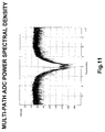
- the utility to have: to compensate the strict requirements on the voltage offset. That is true for all types of ADCs. Furthermore for the only sigma-delta converter the in-band punctual quantization noise is very low, as shown in fig.11, much less than the wished resolution, which instead depends on the integration of the quantization noise over the useful band.
- Fig.11 shows a plot of the Power Spectral Density (PSD) of a multi-path ADC of the two embodiments of the invention.
- PSD Power Spectral Density
- SNR Signal-to-Noise Ratio
- the offsets taken for the various paths are: CH1 Voffset ⁇ -0.00250974 V CH2 Voffset ⁇ -0.0122784 V CH3 Voffset ⁇ 0.00250588 V CH4 Voffset ⁇ 0.00301679 V CH5 Voffset ⁇ 0.00199551 V
- the initial offset mismatch among the various paths is taken sufficiently high.
- the various offsets have been made coincide to the offset of the reference channel CH5 for less than the allowed 22 bit precision.
- the use of the on-line digital calibration technique in any type of ADC, especially sigma-delta converters represents an improvement compared to previous implementations, since it enables to increase the performance of these circuits in terms of speed, while maintaining or improving accuracy.
Landscapes
- Engineering & Computer Science (AREA)
- Theoretical Computer Science (AREA)
- Analogue/Digital Conversion (AREA)
- Compression, Expansion, Code Conversion, And Decoders (AREA)
Priority Applications (3)
| Application Number | Priority Date | Filing Date | Title |
|---|---|---|---|
| EP02425563A EP1401105B1 (fr) | 2002-09-17 | 2002-09-17 | Procédé pour la compensation de tension de décalage pour convertisseurs analogiques-numériques parallèles à entrelacement temporel et circuit pour celui-ci |
| AT02425563T ATE330367T1 (de) | 2002-09-17 | 2002-09-17 | Offsetspannungskompensationsverfahren für parallele zeitverschachtelte analog- digitalwandler sowie schaltung dafür |
| DE60212389T DE60212389T2 (de) | 2002-09-17 | 2002-09-17 | Offsetspannungskompensationsverfahren für parallele zeitverschachtelte Analog-Digitalwandler sowie Schaltung dafür |
Applications Claiming Priority (1)
| Application Number | Priority Date | Filing Date | Title |
|---|---|---|---|
| EP02425563A EP1401105B1 (fr) | 2002-09-17 | 2002-09-17 | Procédé pour la compensation de tension de décalage pour convertisseurs analogiques-numériques parallèles à entrelacement temporel et circuit pour celui-ci |
Publications (2)
| Publication Number | Publication Date |
|---|---|
| EP1401105A1 true EP1401105A1 (fr) | 2004-03-24 |
| EP1401105B1 EP1401105B1 (fr) | 2006-06-14 |
Family
ID=31897011
Family Applications (1)
| Application Number | Title | Priority Date | Filing Date |
|---|---|---|---|
| EP02425563A Expired - Lifetime EP1401105B1 (fr) | 2002-09-17 | 2002-09-17 | Procédé pour la compensation de tension de décalage pour convertisseurs analogiques-numériques parallèles à entrelacement temporel et circuit pour celui-ci |
Country Status (3)
| Country | Link |
|---|---|
| EP (1) | EP1401105B1 (fr) |
| AT (1) | ATE330367T1 (fr) |
| DE (1) | DE60212389T2 (fr) |
Cited By (14)
| Publication number | Priority date | Publication date | Assignee | Title |
|---|---|---|---|---|
| FR2896109A1 (fr) * | 2006-01-06 | 2007-07-13 | Thales Sa | Dispositif de conversion analogique numerique a entrelacement temporel et a egalisation auto adaptative. |
| EP1821413A1 (fr) * | 2006-02-17 | 2007-08-22 | Sicon Semiconductor AB | Convertisseur analogique-numerique a entrelacement temporel |
| WO2008002214A1 (fr) * | 2006-06-30 | 2008-01-03 | Signal Processing Devices Sweden Ab | Système convertisseur analogique-numérique à entrelacement temporel |
| WO2011012812A2 (fr) | 2009-07-30 | 2011-02-03 | Groupe Des Ecoles Des Telecommunications - Ecole Nationale Superieure Des Telecommunications | Correction des défauts analogiques dans des convertisseurs analogiques/numériques parallèles, notamment pour des applications multistandards, radio logicielle et/ou radio-cognitive |
| US8102289B2 (en) * | 2009-02-19 | 2012-01-24 | Hitachi, Ltd. | Analog/digital converter and semiconductor integrated circuit device |
| CN102739252A (zh) * | 2011-04-12 | 2012-10-17 | 美信集成产品公司 | 用于时间交织模数转换器的后台校准的系统和方法 |
| CN102891681A (zh) * | 2012-09-24 | 2013-01-23 | 北京华力创通科技股份有限公司 | 一种多片高速adc芯片的同步方法及装置 |
| CN107636971A (zh) * | 2015-05-29 | 2018-01-26 | 瑞典爱立信有限公司 | 模拟到数字转换器系统 |
| CN108923784A (zh) * | 2018-06-12 | 2018-11-30 | 电子科技大学 | 一种tiadc采集系统的幅频响应误差估计及校正方法 |
| WO2020177646A1 (fr) | 2019-03-01 | 2020-09-10 | Huawei Technologies Co., Ltd. | Architecture de récepteur faisant appel au sous-échantillonnage pour systèmes de communication sans fil |
| WO2021128700A1 (fr) * | 2019-12-26 | 2021-07-01 | 普源精电科技股份有限公司 | Procédé et système d'identification de données échantillonnées par can, circuit intégré et dispositif de décodage |
| CN113574803A (zh) * | 2019-03-29 | 2021-10-29 | 苹果公司 | 校准时间交错模数转换器 |
| US20230318612A1 (en) * | 2022-03-31 | 2023-10-05 | Global Unichip Corporation | Analog-to-digital converting device and method of offset calibration |
| CN113574803B (zh) * | 2019-03-29 | 2024-05-28 | 苹果公司 | 校准时间交错模数转换器 |
Citations (2)
| Publication number | Priority date | Publication date | Assignee | Title |
|---|---|---|---|---|
| US5239299A (en) * | 1991-08-06 | 1993-08-24 | Trw Inc. | Digital equalization of time interleaved analog to digital converters |
| US6414612B1 (en) * | 2000-09-14 | 2002-07-02 | Scientific-Atlanta, Inc. | Enhanced bandwidth digitizer using multiple analog-to digital converters and self calibration |
-
2002
- 2002-09-17 DE DE60212389T patent/DE60212389T2/de not_active Expired - Lifetime
- 2002-09-17 AT AT02425563T patent/ATE330367T1/de not_active IP Right Cessation
- 2002-09-17 EP EP02425563A patent/EP1401105B1/fr not_active Expired - Lifetime
Patent Citations (2)
| Publication number | Priority date | Publication date | Assignee | Title |
|---|---|---|---|---|
| US5239299A (en) * | 1991-08-06 | 1993-08-24 | Trw Inc. | Digital equalization of time interleaved analog to digital converters |
| US6414612B1 (en) * | 2000-09-14 | 2002-07-02 | Scientific-Atlanta, Inc. | Enhanced bandwidth digitizer using multiple analog-to digital converters and self calibration |
Non-Patent Citations (3)
| Title |
|---|
| DYER K ET AL: "Analog background calibration of a 10 b 40 Msample/s parallel pipelined ADC", SOLID-STATE CIRCUITS CONFERENCE, 1998. DIGEST OF TECHNICAL PAPERS. 1998 IEEE INTERNATIONAL SAN FRANCISCO, CA, USA 5-7 FEB. 1998, NEW YORK, NY, USA,IEEE, US, 5 February 1998 (1998-02-05), pages 142 - 143,427, XP010278598, ISBN: 0-7803-4344-1 * |
| FU D ET AL: "DIGITAL BACKGROUND CALIBRATION TECHNIQUE FOR TIME-INTERLEAVED ANALOG-TO-DIGITAL CONVERTERS", IEEE JOURNAL OF SOLID-STATE CIRCUITS, IEEE INC. NEW YORK, US, vol. 33, no. 12, December 1998 (1998-12-01), pages 1904 - 1911, XP000880492, ISSN: 0018-9200 * |
| SONKUSALE S R ET AL: "Background digital error correction technique for pipelined analog-digital converters", ISCAS 2001. PROCEEDINGS OF THE 2001 IEEE INTERNATIONAL SYMPOSIUM ON CIRCUITS AND SYSTEMS. SYDNEY, AUSTRALIA, MAY 6 - 9, 2001, IEEE INTERNATIONAL SYMPOSIUM ON CIRCUITS AND SYSTEMS, NEW YORK, NY: IEEE, US, vol. 1 OF 5, 6 May 2001 (2001-05-06), pages 408 - 411, XP010541453, ISBN: 0-7803-6685-9 * |
Cited By (32)
| Publication number | Priority date | Publication date | Assignee | Title |
|---|---|---|---|---|
| US7466250B2 (en) | 2006-01-06 | 2008-12-16 | Thales | Time interleaved analogue/digital conversion device with self adaptive equalisation |
| EP1811673A1 (fr) * | 2006-01-06 | 2007-07-25 | Thales | Dispositif de conversion analogique numérique à entrelacement temporel et à égalisation auto adaptative |
| FR2896109A1 (fr) * | 2006-01-06 | 2007-07-13 | Thales Sa | Dispositif de conversion analogique numerique a entrelacement temporel et a egalisation auto adaptative. |
| JP2009527167A (ja) * | 2006-02-17 | 2009-07-23 | サイコン セミコンダクター アクティエボラーグ | 時間インターリーブ型アナログ/デジタルコンバータ |
| WO2007093478A1 (fr) * | 2006-02-17 | 2007-08-23 | Sicon Semiconductor Ab | Convertisseur analogique-numérique à entrelacement temporel |
| US7724173B2 (en) | 2006-02-17 | 2010-05-25 | Zoran Corporation | Time-interleaved analog-to-digital-converter |
| EP1821413A1 (fr) * | 2006-02-17 | 2007-08-22 | Sicon Semiconductor AB | Convertisseur analogique-numerique a entrelacement temporel |
| JP4741681B2 (ja) * | 2006-02-17 | 2011-08-03 | ゾラン コーポレイション | 時間インターリーブ型アナログ/デジタルコンバータ |
| WO2008002214A1 (fr) * | 2006-06-30 | 2008-01-03 | Signal Processing Devices Sweden Ab | Système convertisseur analogique-numérique à entrelacement temporel |
| US8307248B2 (en) | 2006-06-30 | 2012-11-06 | Signal Processing Devices Sweden Ab | Method and a system for estimating errors introduced in a time-interleaved analog-to-digital converter system |
| US8736470B2 (en) | 2009-02-19 | 2014-05-27 | Hitachi, Ltd. | Analog/digital converter and semiconductor integrated circuit device |
| US8102289B2 (en) * | 2009-02-19 | 2012-01-24 | Hitachi, Ltd. | Analog/digital converter and semiconductor integrated circuit device |
| US8922407B2 (en) | 2009-02-19 | 2014-12-30 | Hitachi, Ltd. | Analog/digital converter and semiconductor integrated circuit device |
| WO2011012812A2 (fr) | 2009-07-30 | 2011-02-03 | Groupe Des Ecoles Des Telecommunications - Ecole Nationale Superieure Des Telecommunications | Correction des défauts analogiques dans des convertisseurs analogiques/numériques parallèles, notamment pour des applications multistandards, radio logicielle et/ou radio-cognitive |
| JP2013500662A (ja) * | 2009-07-30 | 2013-01-07 | グループ・デ・エコール・デ・テレコミュニカシオン−エコール・ナショナル・シュペリュール・デ・テレコミュニカシオン | 特にマルチスタンダードなソフトウェア無線、および/またはコグニティブ無線の使用のための並列アナログ−デジタル変換器中のアナログ欠陥の訂正方法 |
| CN102739252A (zh) * | 2011-04-12 | 2012-10-17 | 美信集成产品公司 | 用于时间交织模数转换器的后台校准的系统和方法 |
| CN102739252B (zh) * | 2011-04-12 | 2017-03-01 | 马克西姆综合产品公司 | 用于时间交织模数转换器的后台校准的系统和方法 |
| CN102891681A (zh) * | 2012-09-24 | 2013-01-23 | 北京华力创通科技股份有限公司 | 一种多片高速adc芯片的同步方法及装置 |
| CN107636971B (zh) * | 2015-05-29 | 2022-03-01 | 瑞典爱立信有限公司 | 模拟到数字转换器系统 |
| CN107636971A (zh) * | 2015-05-29 | 2018-01-26 | 瑞典爱立信有限公司 | 模拟到数字转换器系统 |
| US10833693B2 (en) | 2015-05-29 | 2020-11-10 | Telefonaktiebolaget Lm Ericsson (Publ) | Time-interleaved analog-to-digital converter system |
| CN108923784A (zh) * | 2018-06-12 | 2018-11-30 | 电子科技大学 | 一种tiadc采集系统的幅频响应误差估计及校正方法 |
| EP3921944A4 (fr) * | 2019-03-01 | 2022-03-30 | Huawei Technologies Co., Ltd. | Architecture de récepteur faisant appel au sous-échantillonnage pour systèmes de communication sans fil |
| CN113498581A (zh) * | 2019-03-01 | 2021-10-12 | 华为技术有限公司 | 用于无线通信系统的基于欠采样的接收器架构 |
| WO2020177646A1 (fr) | 2019-03-01 | 2020-09-10 | Huawei Technologies Co., Ltd. | Architecture de récepteur faisant appel au sous-échantillonnage pour systèmes de communication sans fil |
| CN113498581B (zh) * | 2019-03-01 | 2022-10-11 | 华为技术有限公司 | 用于无线通信系统的基于欠采样的接收器架构 |
| CN113574803A (zh) * | 2019-03-29 | 2021-10-29 | 苹果公司 | 校准时间交错模数转换器 |
| CN113574803B (zh) * | 2019-03-29 | 2024-05-28 | 苹果公司 | 校准时间交错模数转换器 |
| WO2021128700A1 (fr) * | 2019-12-26 | 2021-07-01 | 普源精电科技股份有限公司 | Procédé et système d'identification de données échantillonnées par can, circuit intégré et dispositif de décodage |
| US11438003B2 (en) | 2019-12-26 | 2022-09-06 | Rigol Technologies Co., Ltd. | ADC sampling data identification method and system, integrated circuit and decoding device |
| US20230318612A1 (en) * | 2022-03-31 | 2023-10-05 | Global Unichip Corporation | Analog-to-digital converting device and method of offset calibration |
| US11973511B2 (en) * | 2022-03-31 | 2024-04-30 | Global Unichip Corporation | Analog-to-digital converting device and method of offset calibration |
Also Published As
| Publication number | Publication date |
|---|---|
| ATE330367T1 (de) | 2006-07-15 |
| EP1401105B1 (fr) | 2006-06-14 |
| DE60212389D1 (de) | 2006-07-27 |
| DE60212389T2 (de) | 2007-06-14 |
Similar Documents
| Publication | Publication Date | Title |
|---|---|---|
| CN106888018B (zh) | Dac时序失配误差的数字测量 | |
| US9838031B2 (en) | Dither injection for continuous-time MASH ADCS | |
| CN106888020B (zh) | Dac开关失配误差的数字测量 | |
| EP3182599B1 (fr) | Filtres de suppression du bruit de quantification numérique adaptatif pour convertisseurs analogiques-numériques | |
| Kwak et al. | A 15-b, 5-Msample/s low-spurious CMOS ADC | |
| US7006028B2 (en) | Digital background cancellation of digital to analog converter mismatch noise in analog to digital converters | |
| KR101933575B1 (ko) | 파이프라인형 아날로그 디지털 변환기에서 지연 시간 감소를 위해 수정된 동적 요소 정합 | |
| US20170126239A1 (en) | Noise-shaping successive-approximation-register analog-to-digital converter | |
| EP2719082B1 (fr) | Mise en correspondance d'un élément dynamique modifié afin de réduire le temps d'attente dans un convertisseur analogique-numérique en pipeline | |
| US11329660B2 (en) | VCO-based continuous-time pipelined ADC | |
| EP1401105B1 (fr) | Procédé pour la compensation de tension de décalage pour convertisseurs analogiques-numériques parallèles à entrelacement temporel et circuit pour celui-ci | |
| US6100834A (en) | Recursive multi-bit ADC with predictor | |
| CN108900195B (zh) | 过采样模数转换器及其反馈数模转换器动态误差校准方法 | |
| EP3043478A1 (fr) | Étalonnage assisté par microprocesseur pour convertisseur analogique-numérique | |
| Ferragina et al. | Gain and offset mismatch calibration in time-interleaved multipath A/D sigma-delta modulators | |
| EP3675364A1 (fr) | Compensation de non-concordance dans un convertisseur analogique-numérique à l'aide d'une reconfiguration de trajets de référence | |
| Ferragina et al. | Gain and offset mismatch calibration in multi-path sigma-delta modulators | |
| Loumeau et al. | Analysis of time-interleaved delta-sigma analog to digital converter | |
| Harikumar et al. | A study on switched-capacitor blocks for reconfigurable ADCs | |
| MODULATORS | GAIN AND OFFSET MISMATCH CALIBRATION IN MULTI-PATH SIGMA-DELTA MODULATORS |
Legal Events
| Date | Code | Title | Description |
|---|---|---|---|
| PUAI | Public reference made under article 153(3) epc to a published international application that has entered the european phase |
Free format text: ORIGINAL CODE: 0009012 |
|
| AK | Designated contracting states |
Kind code of ref document: A1 Designated state(s): AT BE BG CH CY CZ DE DK EE ES FI FR GB GR IE IT LI LU MC NL PT SE SK TR |
|
| AX | Request for extension of the european patent |
Extension state: AL LT LV MK RO SI |
|
| 17P | Request for examination filed |
Effective date: 20040920 |
|
| AKX | Designation fees paid |
Designated state(s): AT BE BG CH CY CZ DE DK EE ES FI FR GB GR IE IT LI LU MC NL PT SE SK TR |
|
| GRAP | Despatch of communication of intention to grant a patent |
Free format text: ORIGINAL CODE: EPIDOSNIGR1 |
|
| GRAS | Grant fee paid |
Free format text: ORIGINAL CODE: EPIDOSNIGR3 |
|
| GRAA | (expected) grant |
Free format text: ORIGINAL CODE: 0009210 |
|
| AK | Designated contracting states |
Kind code of ref document: B1 Designated state(s): AT BE BG CH CY CZ DE DK EE ES FI FR GB GR IE IT LI LU MC NL PT SE SK TR |
|
| PG25 | Lapsed in a contracting state [announced via postgrant information from national office to epo] |
Ref country code: AT Free format text: LAPSE BECAUSE OF FAILURE TO SUBMIT A TRANSLATION OF THE DESCRIPTION OR TO PAY THE FEE WITHIN THE PRESCRIBED TIME-LIMIT Effective date: 20060614 Ref country code: IT Free format text: LAPSE BECAUSE OF FAILURE TO SUBMIT A TRANSLATION OF THE DESCRIPTION OR TO PAY THE FEE WITHIN THE PRESCRIBED TIME-LIMIT;WARNING: LAPSES OF ITALIAN PATENTS WITH EFFECTIVE DATE BEFORE 2007 MAY HAVE OCCURRED AT ANY TIME BEFORE 2007. THE CORRECT EFFECTIVE DATE MAY BE DIFFERENT FROM THE ONE RECORDED. Effective date: 20060614 Ref country code: SK Free format text: LAPSE BECAUSE OF FAILURE TO SUBMIT A TRANSLATION OF THE DESCRIPTION OR TO PAY THE FEE WITHIN THE PRESCRIBED TIME-LIMIT Effective date: 20060614 Ref country code: FI Free format text: LAPSE BECAUSE OF FAILURE TO SUBMIT A TRANSLATION OF THE DESCRIPTION OR TO PAY THE FEE WITHIN THE PRESCRIBED TIME-LIMIT Effective date: 20060614 Ref country code: LI Free format text: LAPSE BECAUSE OF FAILURE TO SUBMIT A TRANSLATION OF THE DESCRIPTION OR TO PAY THE FEE WITHIN THE PRESCRIBED TIME-LIMIT Effective date: 20060614 Ref country code: CH Free format text: LAPSE BECAUSE OF FAILURE TO SUBMIT A TRANSLATION OF THE DESCRIPTION OR TO PAY THE FEE WITHIN THE PRESCRIBED TIME-LIMIT Effective date: 20060614 Ref country code: NL Free format text: LAPSE BECAUSE OF FAILURE TO SUBMIT A TRANSLATION OF THE DESCRIPTION OR TO PAY THE FEE WITHIN THE PRESCRIBED TIME-LIMIT Effective date: 20060614 Ref country code: BE Free format text: LAPSE BECAUSE OF FAILURE TO SUBMIT A TRANSLATION OF THE DESCRIPTION OR TO PAY THE FEE WITHIN THE PRESCRIBED TIME-LIMIT Effective date: 20060614 |
|
| REG | Reference to a national code |
Ref country code: GB Ref legal event code: FG4D |
|
| REG | Reference to a national code |
Ref country code: CH Ref legal event code: EP |
|
| RAP2 | Party data changed (patent owner data changed or rights of a patent transferred) |
Owner name: SIEMENS S.P.A. |
|
| REG | Reference to a national code |
Ref country code: IE Ref legal event code: FG4D |
|
| REF | Corresponds to: |
Ref document number: 60212389 Country of ref document: DE Date of ref document: 20060727 Kind code of ref document: P |
|
| NLT2 | Nl: modifications (of names), taken from the european patent patent bulletin |
Owner name: SIEMENS S.P.A. Effective date: 20060621 |
|
| PG25 | Lapsed in a contracting state [announced via postgrant information from national office to epo] |
Ref country code: SE Free format text: LAPSE BECAUSE OF FAILURE TO SUBMIT A TRANSLATION OF THE DESCRIPTION OR TO PAY THE FEE WITHIN THE PRESCRIBED TIME-LIMIT Effective date: 20060914 Ref country code: DK Free format text: LAPSE BECAUSE OF FAILURE TO SUBMIT A TRANSLATION OF THE DESCRIPTION OR TO PAY THE FEE WITHIN THE PRESCRIBED TIME-LIMIT Effective date: 20060914 |
|
| PG25 | Lapsed in a contracting state [announced via postgrant information from national office to epo] |
Ref country code: IE Free format text: LAPSE BECAUSE OF NON-PAYMENT OF DUE FEES Effective date: 20060918 |
|
| PG25 | Lapsed in a contracting state [announced via postgrant information from national office to epo] |
Ref country code: ES Free format text: LAPSE BECAUSE OF FAILURE TO SUBMIT A TRANSLATION OF THE DESCRIPTION OR TO PAY THE FEE WITHIN THE PRESCRIBED TIME-LIMIT Effective date: 20060925 |
|
| PG25 | Lapsed in a contracting state [announced via postgrant information from national office to epo] |
Ref country code: MC Free format text: LAPSE BECAUSE OF NON-PAYMENT OF DUE FEES Effective date: 20060930 |
|
| PG25 | Lapsed in a contracting state [announced via postgrant information from national office to epo] |
Ref country code: PT Free format text: LAPSE BECAUSE OF FAILURE TO SUBMIT A TRANSLATION OF THE DESCRIPTION OR TO PAY THE FEE WITHIN THE PRESCRIBED TIME-LIMIT Effective date: 20061114 |
|
| NLV1 | Nl: lapsed or annulled due to failure to fulfill the requirements of art. 29p and 29m of the patents act | ||
| REG | Reference to a national code |
Ref country code: CH Ref legal event code: PL |
|
| PLBE | No opposition filed within time limit |
Free format text: ORIGINAL CODE: 0009261 |
|
| STAA | Information on the status of an ep patent application or granted ep patent |
Free format text: STATUS: NO OPPOSITION FILED WITHIN TIME LIMIT |
|
| EN | Fr: translation not filed | ||
| 26N | No opposition filed |
Effective date: 20070315 |
|
| PGFP | Annual fee paid to national office [announced via postgrant information from national office to epo] |
Ref country code: CZ Payment date: 20070913 Year of fee payment: 6 |
|
| PGFP | Annual fee paid to national office [announced via postgrant information from national office to epo] |
Ref country code: BG Payment date: 20070917 Year of fee payment: 6 |
|
| PG25 | Lapsed in a contracting state [announced via postgrant information from national office to epo] |
Ref country code: GR Free format text: LAPSE BECAUSE OF FAILURE TO SUBMIT A TRANSLATION OF THE DESCRIPTION OR TO PAY THE FEE WITHIN THE PRESCRIBED TIME-LIMIT Effective date: 20060915 Ref country code: FR Free format text: LAPSE BECAUSE OF FAILURE TO SUBMIT A TRANSLATION OF THE DESCRIPTION OR TO PAY THE FEE WITHIN THE PRESCRIBED TIME-LIMIT Effective date: 20070309 |
|
| PG25 | Lapsed in a contracting state [announced via postgrant information from national office to epo] |
Ref country code: EE Free format text: LAPSE BECAUSE OF FAILURE TO SUBMIT A TRANSLATION OF THE DESCRIPTION OR TO PAY THE FEE WITHIN THE PRESCRIBED TIME-LIMIT Effective date: 20060614 |
|
| PG25 | Lapsed in a contracting state [announced via postgrant information from national office to epo] |
Ref country code: LU Free format text: LAPSE BECAUSE OF NON-PAYMENT OF DUE FEES Effective date: 20060917 Ref country code: TR Free format text: LAPSE BECAUSE OF FAILURE TO SUBMIT A TRANSLATION OF THE DESCRIPTION OR TO PAY THE FEE WITHIN THE PRESCRIBED TIME-LIMIT Effective date: 20060614 |
|
| PG25 | Lapsed in a contracting state [announced via postgrant information from national office to epo] |
Ref country code: FR Free format text: LAPSE BECAUSE OF FAILURE TO SUBMIT A TRANSLATION OF THE DESCRIPTION OR TO PAY THE FEE WITHIN THE PRESCRIBED TIME-LIMIT Effective date: 20060614 Ref country code: CY Free format text: LAPSE BECAUSE OF FAILURE TO SUBMIT A TRANSLATION OF THE DESCRIPTION OR TO PAY THE FEE WITHIN THE PRESCRIBED TIME-LIMIT Effective date: 20060614 |
|
| PGFP | Annual fee paid to national office [announced via postgrant information from national office to epo] |
Ref country code: GB Payment date: 20080918 Year of fee payment: 7 |
|
| PG25 | Lapsed in a contracting state [announced via postgrant information from national office to epo] |
Ref country code: CZ Free format text: LAPSE BECAUSE OF NON-PAYMENT OF DUE FEES Effective date: 20080917 |
|
| GBPC | Gb: european patent ceased through non-payment of renewal fee |
Effective date: 20090917 |
|
| PG25 | Lapsed in a contracting state [announced via postgrant information from national office to epo] |
Ref country code: BG Free format text: LAPSE BECAUSE OF NON-PAYMENT OF DUE FEES Effective date: 20080930 Ref country code: GB Free format text: LAPSE BECAUSE OF NON-PAYMENT OF DUE FEES Effective date: 20090917 |
|
| PGFP | Annual fee paid to national office [announced via postgrant information from national office to epo] |
Ref country code: DE Payment date: 20120921 Year of fee payment: 11 |
|
| REG | Reference to a national code |
Ref country code: DE Ref legal event code: R082 Ref document number: 60212389 Country of ref document: DE |
|
| REG | Reference to a national code |
Ref country code: DE Ref legal event code: R081 Ref document number: 60212389 Country of ref document: DE Owner name: NOKIA SIEMENS NETWORKS ITALIA S.P.A., IT Free format text: FORMER OWNER: SIEMENS MOBILE COMMUNICATIONS S.P.A., MAILAND/MILANO, IT Effective date: 20130620 |
|
| REG | Reference to a national code |
Ref country code: DE Ref legal event code: R119 Ref document number: 60212389 Country of ref document: DE Effective date: 20140401 |
|
| PG25 | Lapsed in a contracting state [announced via postgrant information from national office to epo] |
Ref country code: DE Free format text: LAPSE BECAUSE OF NON-PAYMENT OF DUE FEES Effective date: 20140401 |