EP1383176A1 - Iii group nitride compound semiconductor luminescent element - Google Patents

Iii group nitride compound semiconductor luminescent element Download PDF

Info

Publication number
EP1383176A1
EP1383176A1 EP02720559A EP02720559A EP1383176A1 EP 1383176 A1 EP1383176 A1 EP 1383176A1 EP 02720559 A EP02720559 A EP 02720559A EP 02720559 A EP02720559 A EP 02720559A EP 1383176 A1 EP1383176 A1 EP 1383176A1
Authority
EP
European Patent Office
Prior art keywords
layer
intermediate layer
emitting device
ingan
compound semiconductor
Prior art date
Legal status (The legal status is an assumption and is not a legal conclusion. Google has not performed a legal analysis and makes no representation as to the accuracy of the status listed.)
Granted
Application number
EP02720559A
Other languages
German (de)
French (fr)
Other versions
EP1383176B1 (en
EP1383176A4 (en
Inventor
Shinya c/o Toyoda Gosei Co. Ltd. ASAMI
Hiroshi c/o Toyoda Gosei Co. Ltd. Watanabe
Jun c/o Toyoda Gosei Co. Ltd. ITO
Naoki c/o Toyoda Gosei Co. Ltd. SHIBATA
Current Assignee (The listed assignees may be inaccurate. Google has not performed a legal analysis and makes no representation or warranty as to the accuracy of the list.)
Toyoda Gosei Co Ltd
Original Assignee
Toyoda Gosei Co Ltd
Priority date (The priority date is an assumption and is not a legal conclusion. Google has not performed a legal analysis and makes no representation as to the accuracy of the date listed.)
Filing date
Publication date
Application filed by Toyoda Gosei Co Ltd filed Critical Toyoda Gosei Co Ltd
Publication of EP1383176A1 publication Critical patent/EP1383176A1/en
Publication of EP1383176A4 publication Critical patent/EP1383176A4/en
Application granted granted Critical
Publication of EP1383176B1 publication Critical patent/EP1383176B1/en
Anticipated expiration legal-status Critical
Expired - Lifetime legal-status Critical Current

Links

Images

Classifications

    • HELECTRICITY
    • H10SEMICONDUCTOR DEVICES; ELECTRIC SOLID-STATE DEVICES NOT OTHERWISE PROVIDED FOR
    • H10HINORGANIC LIGHT-EMITTING SEMICONDUCTOR DEVICES HAVING POTENTIAL BARRIERS
    • H10H20/00Individual inorganic light-emitting semiconductor devices having potential barriers, e.g. light-emitting diodes [LED]
    • H10H20/80Constructional details
    • H10H20/81Bodies
    • H10H20/822Materials of the light-emitting regions
    • H10H20/824Materials of the light-emitting regions comprising only Group III-V materials, e.g. GaP
    • H10H20/825Materials of the light-emitting regions comprising only Group III-V materials, e.g. GaP containing nitrogen, e.g. GaN
    • BPERFORMING OPERATIONS; TRANSPORTING
    • B82NANOTECHNOLOGY
    • B82YSPECIFIC USES OR APPLICATIONS OF NANOSTRUCTURES; MEASUREMENT OR ANALYSIS OF NANOSTRUCTURES; MANUFACTURE OR TREATMENT OF NANOSTRUCTURES
    • B82Y20/00Nanooptics, e.g. quantum optics or photonic crystals
    • HELECTRICITY
    • H10SEMICONDUCTOR DEVICES; ELECTRIC SOLID-STATE DEVICES NOT OTHERWISE PROVIDED FOR
    • H10HINORGANIC LIGHT-EMITTING SEMICONDUCTOR DEVICES HAVING POTENTIAL BARRIERS
    • H10H20/00Individual inorganic light-emitting semiconductor devices having potential barriers, e.g. light-emitting diodes [LED]
    • H10H20/01Manufacture or treatment
    • H10H20/011Manufacture or treatment of bodies, e.g. forming semiconductor layers
    • H10H20/013Manufacture or treatment of bodies, e.g. forming semiconductor layers having light-emitting regions comprising only Group III-V materials
    • H10H20/0133Manufacture or treatment of bodies, e.g. forming semiconductor layers having light-emitting regions comprising only Group III-V materials with a substrate not being Group III-V materials
    • H10H20/01335Manufacture or treatment of bodies, e.g. forming semiconductor layers having light-emitting regions comprising only Group III-V materials with a substrate not being Group III-V materials the light-emitting regions comprising nitride materials
    • HELECTRICITY
    • H10SEMICONDUCTOR DEVICES; ELECTRIC SOLID-STATE DEVICES NOT OTHERWISE PROVIDED FOR
    • H10HINORGANIC LIGHT-EMITTING SEMICONDUCTOR DEVICES HAVING POTENTIAL BARRIERS
    • H10H20/00Individual inorganic light-emitting semiconductor devices having potential barriers, e.g. light-emitting diodes [LED]
    • H10H20/80Constructional details
    • H10H20/81Bodies
    • H10H20/811Bodies having quantum effect structures or superlattices, e.g. tunnel junctions
    • H10H20/812Bodies having quantum effect structures or superlattices, e.g. tunnel junctions within the light-emitting regions, e.g. having quantum confinement structures
    • YGENERAL TAGGING OF NEW TECHNOLOGICAL DEVELOPMENTS; GENERAL TAGGING OF CROSS-SECTIONAL TECHNOLOGIES SPANNING OVER SEVERAL SECTIONS OF THE IPC; TECHNICAL SUBJECTS COVERED BY FORMER USPC CROSS-REFERENCE ART COLLECTIONS [XRACs] AND DIGESTS
    • Y10TECHNICAL SUBJECTS COVERED BY FORMER USPC
    • Y10STECHNICAL SUBJECTS COVERED BY FORMER USPC CROSS-REFERENCE ART COLLECTIONS [XRACs] AND DIGESTS
    • Y10S257/00Active solid-state devices, e.g. transistors, solid-state diodes
    • Y10S257/918Light emitting regenerative switching device, e.g. light emitting scr arrays, circuitry

Definitions

  • the present invention relates to a Group III nitride compound semiconductor light-emitting device. Particularly, it relates to a Group III nitride compound semiconductor light-emitting device for emitting light at a relatively short wavelength.
  • a Group III nitride compound semiconductor light-emitting device is known as a light-emitting diode for emitting light in a color ranging from blue to green.
  • the Group III nitride compound semiconductor light-emitting device is also used as a light-emitting diode for emitting light at a shorter wavelength (in a range of from near-ultraviolet to ultraviolet) than the wavelength of visible light.
  • Group III nitride compound semiconductor light-emitting device emitting light at such a short wavelength is heretofore known, higher light-emitting efficiency and output have been requiredof the light-emitting device recently.
  • a light-emitting device having the following configuration has been conceived. That is, there is provided a Group III nitride compound semiconductor light-emitting device including: a multilayer containing a quantum well structure having an InGaN well layer and an AlGaN barrier layer; and an intermediate layer of InGaN thicker than the InGaN well layer and disposed below the multilayer.
  • Group III nitride compound semiconductor light-emitting device configured as described above; light at a short wavelength, e.g., a wavelength of 360-550 nm can be emitted with a high output compared with the conventional device.
  • a multilayer containing a quantum well structure having an InGaN well layer and an AlGaN barrier layer is employed, and the film thickness, growth rate and growth temperature of each of the InGaN layers as the well layers and the film thickness of each of the AlGaN layers as the barrier layers are controlled to be optimized. Accordingly, the output of the Group IIInitride compound semiconductor light-emitting device is improved.
  • the intermediate layer which serves as an undercoat layer for the multilayer is also optimized. Also from this point of view, improvement in output of the Group III nitride compound semiconductor light-emitting device is attained.
  • the wavelength range aiming at improving the light-emitting output is 360-550 nm but the wavelength range is not particularly limited.
  • the wavelength range aiming at improving the light-emitting output in the invention is more preferably 360-520 nm, more and more preferably 360-490 nm, more andmore andmore preferably 360-460 nm, most preferably 360-430 nm.
  • each Group III nitride compound semiconductor is represented by the general formula Al X Ga Y In 1-X-Y N (0 ⁇ X ⁇ 1, 0 ⁇ Y ⁇ 1, 0 ⁇ X+Y ⁇ 1) which includes so-called binary compounds such as AlN, GaN and InN, and so-called ternary compounds such as Al x Ga 1-x N, Al x In 1-x N and Ga X In 1-x N (0 ⁇ x ⁇ 1 in the above).
  • the group III elements may be at least partially replaced by boron (B), thallium (Tl), or the like.
  • the nitrogen (N) may be at least partially replaced by phosphorus (P), arsenic (As), antimony (Sb), bismuth (Bi), or the like.
  • Each Group III nitride compound semiconductor layer may contain an optional dopant.
  • Si, Ge, Se, Te, C, or the like can be used as n-type impurities.
  • Mg, Zn, Be, Ca, Sr, Ba, or the like can be used as p-type impurities.
  • the Group III nitride compound semiconductor may be subjected to electron beam irradiation, plasma irradiation or heating due to a furnace but this process is not essential.
  • Amethod for forming the Group III nitride compound semiconductor layer is not particularly limited.
  • the Group III nitride compound semiconductor layer can be formed by a known method such as a molecular beam epitaxy method (MBE method) , a halide vapor phase epitaxy method (HVPE method), a sputtering method, an ion-plating method, an electron showering method, or the like.
  • MBE method molecular beam epitaxy method
  • HVPE method halide vapor phase epitaxy method
  • sputtering method an ion-plating method
  • an electron showering method or the like.
  • the multilayer contains an InGaN well layer and anAlGaNbarrier layer which is a light-emitting layer.
  • the multilayer has a laminated structure in which each of the InGaN well layers is sandwiched between AlGaN layers.
  • the multilayer is configured so that a unit pair made of a laminate of an AlGaN layer and an InGaN well layer is laminated or two or more unit pairs are laminated, and an AlGaN layer or a GaN layer is finally laminated.
  • the p-type layer side uppermost layer is an AlGaN layer or a GaN layer.
  • the intermediate layer side lowermost layer is also an AlGaN layer or a GaN layer.
  • a combination of the uppermost layer of AlGaN and the lowermost layer of AlGaN, a combination of the uppermost layer of AlGaN and the lowermost layer of GaN or a combination of the uppermost layer of GaN and the lowermost layer of GaN is preferable.
  • the number of unit pairs is selected to be preferably 1-10, more preferably 2-8, more and more preferably 3-7, more and more and more preferably 3-6, most preferably 3.5.
  • the wavelength of emitted light entirely depends on the compositional ratio of In and Ga in the InGaN well layer.
  • the compositional ratio of In is selected to be preferably 1-20 %, more preferably 1-15 %, more and more preferably 1-10 %, most preferably 1-8 %.
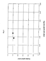
  • Fig. 1 shows the relation between the film thickness of each InGaN layer as a well layer and the light-emitting intensity of the light-emitting device at 20 mA (hereinafter, the light-emitting intensity of the light-emitting device expresses light-emitting intensity at the time of application of 20 mA if no special notice is given).
  • a result of Fig. 1 is obtained when the thickness of each of InGaN well layers forming the multilayer is changed as shown in the horizontal axis in the light-emitting device 1 shown in Embodiments (see Figs. and 7).
  • each InGaN well layer is selected to be preferably 90-200 ⁇ (9.0-20.0 nm), more preferably 100-175 ⁇ (10.0-17.5 nm).
  • Fig. 2 shows the relation between the growth rate of each InGaN well layer and the light-emitting intensity of the light-emitting device.
  • FIG. 2 A result of Fig. 2 is obtained when the growth rate of .each of InGaN well layers forming the multilayer is changed as shown in the horizontal axis in the light-emitting device shown in Embodiments.
  • each InGaN well layer is selected to be preferably 0.25-0.35 ⁇ /s (0.025-0.035 nm/s).
  • the flow rate of material gas (TMG, TMI, ammonia) is changed to control the growth rate.
  • Fig. 3 shows the relation between the growth temperature of each InGaN well layer and the light-emitting intensity of the light-emitting device.
  • FIG. 3 A result of Fig. 3 is obtained when the growth temperature of each of InGaN well layers forming the multilayer is changed as shown in the horizontal axis in the light-emitting device shown in Embodiments.
  • the growth temperature of each InGaN well layer is selected to be preferably 770-790°C, more preferably 777-783°C.
  • Fig. 4 shows the relation between the film thickness of each AlGaN layer as a barrier layer and the light-emitting intensity of the light-emitting device.
  • a result of Fig. 4 is obtained when the thickness of each AlGaN layer is changed as shown in the horizontal axis in the light-emitting device shown in Embodiments.
  • each AlGaN layer is selected to be preferably 50-125 ⁇ (5.0-12.5 nm).
  • the uppermost layer in the multilayer is preferably formed to be thicker by 10-30 % than any other barrier layers because the uppermost layer serves as a cap layer.
  • an intermediate layer under the multilayer is obtained by laminating a first intermediate layer of InGaN, a second intermediate layer of GaN and a third intermediate layer of AlGaN successively.
  • each of the first, second and third intermediate layers is not doped.
  • the third intermediate layer of AlGaN may.be omitted. If the second intermediate layer of GaN is omitted, the third intermediate layer of AlGaNbecomes the second intermediate layer.
  • the second intermediate layer may be also regarded as a laminate of a GaN layer and an AlGaN layer.
  • Fig. 5 shows the relation between the growth temperature of the first intermediate layer of InGaN and the light-emitting intensity of the light-emitting device.
  • FIG. 5 A result of Fig. 5 is obtained when the growth temperature of the first intermediate layer of InGaN is changed as shown in the horizontal axis in the light-emitting device shown in Embodiments.
  • the growth temperature of the first intermediate layer of InGaN is selected to be preferably 770-875°C, more preferably 800-850°C.
  • a preferred light-emitting output is obtained also when the InGaN well layers and the AlGaN barrier layers are provided in the following conditions. That is, in the conditions shown in Figs. 10, 11 and 12, a preferred light-emitting output is obtained particularly at a wavelength of 360-430 nm.
  • FIG. 10 A result of Fig. 10 is obtained when the thickness of each of InGaN well layers forming the multilayer is changed as shown in the horizontal axis in the light-emitting device 1 shown in Embodiments (see Figs. 6 and 7). It is obvious from the result of Fig. 10 that the film thickness of each InGaN well layer is selected to be preferably 20-60 ⁇ (2.0-6.0 nm), more preferably 35-50 ⁇ (3.5-5.0 nm).
  • a result of Fig. 11 is obtained when the growth rate of each of InGaN well layers forming the multilayer is changed as shown in the horizontal axis in the light-emitting device shown in Embodiments. It is obvious from the result of Fig. 11 that the growth rate of each InGaN well layer is selected to be preferably 0.08-0.18 ⁇ /s (0.008-0.018 nm/s). For obtaining the result of Fig. 11, the flow rate of material gas (TMG, TMI, ammonia) is changed to control the growth rate.
  • TMG material gas
  • each barrier layer is preferably formed to be thicker than each well layer.
  • Fig. 6 shows a semiconductor laminated structure of a light-emitting diode 1 according to this embodiment.
  • carrier concentration is as follows.
  • the carrier concentration in the second p-type layer 17 is not lower than 1 X 10 17 /cm 3 .
  • the carrier concentration in the first p-type layer 16 is 0.5-2.0 X 10 17 /cm 3 .
  • the intermediate layers 14a to 14c are substantially not doped.
  • the carrier concentration in the n-type layer 13 is not lower than 1.0 X 10 18 /cm 3 .
  • the substrate temperature (growth temperature) of the n-type layer 13, the first p-type layer 16 and the second p-type layer 17 is selected to be not lower than 1000°C.
  • a so-called low-temperature buffer layer can be used as the buffer layer
  • a high-temperature buffer layer is employed in this embodiment (see Unexamined Japanese Patent Publication No. 2001-015443).
  • the light-emitting diode configured as described above is produced as follows.
  • the sapphire substrate 11 is heated to 1130°C so that a surface (face a ) is cleaned.
  • TMA and NH 3 are introduced and the buffer layer 12 of AlN is grown by an MOCVD method.
  • the n-type layer 13 is formed and Group III nitride compound semiconductor layers 14 to 17 following the n-type layer 13 are formed according to an ordinarymethod (MOCVD method).
  • an ammonia gas and gases of Group III element alkyl compounds such as trimethylgallium (TMG), trimethylaluminum (TMA) andtrimethylindium (TMI) are supplied onto the substrate heated to an appropriate temperature and are subjected to a heat decomposition reaction to thereby grow a desired crystal on the substrate.
  • Group III element alkyl compounds such as trimethylgallium (TMG), trimethylaluminum (TMA) andtrimethylindium (TMI) are supplied onto the substrate heated to an appropriate temperature and are subjected to a heat decomposition reaction to thereby grow a desired crystal on the substrate.
  • Silane or disilane is used for introducing silicon (Si) as impurities.
  • (RC 5 H 4 ) 2 Mg is used for introducing magnesium (Mg) as impurities.
  • the substrate temperature for growing the first intermediate 14a is preferably selected to be 770-875°C (see Fig. 5). In this embodiment, the substrate temperature is selected to be 800°C.
  • the substrate temperature for growing each InGaN well layer 15b in the multilayer 15 is preferably selected to be 770-790°C as shown in Fig. 3. In this embodiment; the substrate temperature is selected to be 780°C.
  • the growth temperature of the AlGaN layer 15a in the multilayer 15 is not particularly limited if the well layer containing indium (In) is not eliminated at this temperature.
  • the substrate temperature is selected to be 885°C.
  • the substrate temperature of the first p-type layer 16 and the second p-type layer 17 is kept at 1000°C.
  • the semiconductor layers are partially removed by reactive ion etching to thereby reveal the n-type layer 13 on which an n-electrode pad 21 will be formed (see Fig. 7).
  • a photo resist is applied on a semiconductor surface uniformly.
  • the photo resist is removed from an electrode-forming portion on the second p-type layer 17 by photolithography to thereby reveal the portion of the second p-type layer 17.
  • An Au-Co translucent electrode layer 19 is formed on the revealed second p-type layer 17 by an evaporation apparatus.
  • a p-electrode pad 20 and an n-electrode pad 21 are vapor-deposited in the same manner as described above.
  • Short-wavelength light having a peak wavelength of 382 nm is emitted efficiently from the light-emitting diode configured as described above.
  • This embodiment is configured in the same manner as in the first embodiment except that the lowermost layer 15a' o.f the multilayer 15 in the device according to the first embodiment is made of GaN as shown in Fig. 8.
  • short-wavelength light having a peak wavelength of 382 nm is emitted efficiently.
  • This embodiment is configured in the same manner as in the first embodiment except that the lowermost layer 15a' of the multilayer 15 in the device according to the first embodiment is made of GaN and the upper most layer 15d' thereof is made of GaN as shown in Fig. 9.
  • short-wavelength light having a peak wavelength of 382 nm is emitted efficiently.
  • the semiconductor configuration of a light-emitting diode according to this embodiment is the same as shown in Fig. 6. Specifications of respective layers are as follows. Layer Composition:Dopant (Thickness) Second p-type layer 17 p-Al 0.02 Ga 0.98 N:Mg (75 nm) First p-type layer 16 p-Al 0.10-0.45 Ga 0.90-0.55 N:Mg (smaller than 70 nm) Multilayer 15 Uppermost layer 15d Al 0.04-0.20 Ga 0.96-0.80 N (5-18.0 nm) Barrier layer 15c Al 0.04-0.20 Ga 0.96-0.80 N (5-13.5 nm) Well layer 15b In 0.01-0.20 Ga 0.99-0.80 N (2-6 nm) Lowermost layer 15a Al 0.04-0.20 Ga 0.96-0.80 N (5-13.5 nm) Third intermediate layer 14c Al 0.10-0.45 Ga 0.90-0.55 N (10 nm) Second intermediate layer 14b GaN (10 nm) First intermediate layer 14a In
  • carrier concentration is as follows.
  • the carrier concentration in the second p-type layer 17 is not lower than 5 X 10 16 /cm 3 .
  • the carrier concentration in the first p-type layer 16 is 0.5-2.0 X 10 17 /cm 3 .
  • the intermediate layers 14a to 14c are substantially not doped.
  • the carrier concentration in the n-type layer 13 is not lower than 1.0 X 10 18 /cm 3 .

Landscapes

  • Chemical & Material Sciences (AREA)
  • Engineering & Computer Science (AREA)
  • Nanotechnology (AREA)
  • Physics & Mathematics (AREA)
  • Life Sciences & Earth Sciences (AREA)
  • Biophysics (AREA)
  • Optics & Photonics (AREA)
  • Crystallography & Structural Chemistry (AREA)
  • Led Devices (AREA)
  • Semiconductor Lasers (AREA)

Abstract

A Group III nitride compound semiconductor light-emitting device includes a multilayer having a quantum well structure containing an InGaN well layer and an AlGaN barrier layer. The film thickness, growth rate and growth temperature of the InGaN layer as the well layer and the film thickness of the AlGaN layer as the barrier layer are controlled to be optimized to thereby improve an output of the light-emitting device.

Description

Technical Field
The present invention relates to a Group III nitride compound semiconductor light-emitting device. Particularly, it relates to a Group III nitride compound semiconductor light-emitting device for emitting light at a relatively short wavelength.
Background Art
A Group III nitride compound semiconductor light-emitting device is known as a light-emitting diode for emitting light in a color ranging from blue to green. The Group III nitride compound semiconductor light-emitting device is also used as a light-emitting diode for emitting light at a shorter wavelength (in a range of from near-ultraviolet to ultraviolet) than the wavelength of visible light.
Although the Group III nitride compound semiconductor light-emitting device emitting light at such a short wavelength is heretofore known, higher light-emitting efficiency and output have been requiredof the light-emitting device recently.
Disclosure of the Invention
The present inventors have made eager examination to improve the Group III nitride compound semiconductor light-emitting device emitting light at a short wavelength. As a result, a light-emitting device having the following configuration has been conceived. That is, there is provided a Group III nitride compound semiconductor light-emitting device including: a multilayer containing a quantum well structure having an InGaN well layer and an AlGaN barrier layer; and an intermediate layer of InGaN thicker than the InGaN well layer and disposed below the multilayer.
According to the Group III nitride compound semiconductor light-emitting device configured as described above; light at a short wavelength, e.g., a wavelength of 360-550 nm can be emitted with a high output compared with the conventional device.
Moreover, a multilayer containing a quantum well structure having an InGaN well layer and an AlGaN barrier layer is employed, and the film thickness, growth rate and growth temperature of each of the InGaN layers as the well layers and the film thickness of each of the AlGaN layers as the barrier layers are controlled to be optimized. Accordingly, the output of the Group IIInitride compound semiconductor light-emitting device is improved.
In addition, the intermediate layer which serves as an undercoat layer for the multilayer is also optimized. Also from this point of view, improvement in output of the Group III nitride compound semiconductor light-emitting device is attained.
Brief Description of the Drawings
  • Fig. 1 shows the relation between the film thickness of each InGaN layer as a well layer and the light-emitting intensity of a light-emitting device;
  • Fig. 2 shows the relation between the growth rate of each InGaN well layer and the light-emitting intensity of the light-emitting device;
  • Fig. 3 shows the relation between the growth temperature of each InGaN well layer and the light-emitting intensity of the light-emitting device;
  • Fig. 4 shows the relation between the film thickness of each AlGaN layer as a barrier layer and the light-emitting intensity of the light-emitting device;
  • Fig. 5 shows the relation between the growth temperature of a first intermediate layer of InGaN and the light-emitting intensity of the light-emitting device;
  • Fig. 6 shows Group III nitride compound semiconductor layers in a light-emitting device according to.an embodiment of the invention;
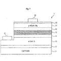
  • Fig. 7 shows a configuration of the light-emitting device according to this embodiment of the invention;
  • Fig. 8 shows Group III nitride compound semiconductor layers in a light-emitting device according to another embodiment;
  • Fig. 9 shows Group III nitride compound semiconductor layers in a light-emitting device according to a further embodiment;
  • Fig. 10 shows the relation between the film thickness of each InGaN layer as a well layer and the light-emitting intensity of a light-emitting device;
  • Fig: 11 shows the relation between the growth rate of each InGaN well layer and the light-emitting intensity of the light-emitting device; and
  • Fig. 12 shows the relation between the film thickness of each AlGaN layer as a barrier layer and the light-emitting intensity of the light-emitting device.
  • Best Mode for Carrying Out the Invention
    The present invention will be described below in detail.
    According to an aspect of the invention, the wavelength range aiming at improving the light-emitting output is 360-550 nm but the wavelength range is not particularly limited. The wavelength range aiming at improving the light-emitting output in the invention is more preferably 360-520 nm, more and more preferably 360-490 nm, more andmore andmore preferably 360-460 nm, most preferably 360-430 nm.
    In this description, each Group III nitride compound semiconductor is represented by the general formula AlXGaYIn1-X-YN (0≤X≤1, 0≤Y≤1, 0≤X+Y≤1) which includes so-called binary compounds such as AlN, GaN and InN, and so-called ternary compounds such as AlxGa1-xN, AlxIn1-xN and GaXIn1-xN (0<x<1 in the above). The group III elements may be at least partially replaced by boron (B), thallium (Tl), or the like. The nitrogen (N) may be at least partially replaced by phosphorus (P), arsenic (As), antimony (Sb), bismuth (Bi), or the like. Each Group III nitride compound semiconductor layer may contain an optional dopant. Si, Ge, Se, Te, C, or the like, can be used as n-type impurities. Mg, Zn, Be, Ca, Sr, Ba, or the like, can be used as p-type impurities. Incidentally, after doped with p-type impurities, the Group III nitride compound semiconductor may be subjected to electron beam irradiation, plasma irradiation or heating due to a furnace but this process is not essential. Amethod for forming the Group III nitride compound semiconductor layer is not particularly limited. Besides a metal organic chemical vapor deposition method (MOCVD method), the Group III nitride compound semiconductor layer can be formed by a known method such as a molecular beam epitaxy method (MBE method) , a halide vapor phase epitaxy method (HVPE method), a sputtering method, an ion-plating method, an electron showering method, or the like.
    In this invention, specific Group III nitride compound semiconductors are used for forming specific layers respectively.
    In the invention, the multilayer contains an InGaN well layer and anAlGaNbarrier layer which is a light-emitting layer. The multilayer has a laminated structure in which each of the InGaN well layers is sandwiched between AlGaN layers.
    In another aspect, the multilayer is configured so that a unit pair made of a laminate of an AlGaN layer and an InGaN well layer is laminated or two or more unit pairs are laminated, and an AlGaN layer or a GaN layer is finally laminated. That is, the p-type layer side uppermost layer is an AlGaN layer or a GaN layer. On the other hand, the intermediate layer side lowermost layer is also an AlGaN layer or a GaN layer. A combination of the uppermost layer of AlGaN and the lowermost layer of AlGaN, a combination of the uppermost layer of AlGaN and the lowermost layer of GaN or a combination of the uppermost layer of GaN and the lowermost layer of GaN is preferable.
    The number of unit pairs is selected to be preferably 1-10, more preferably 2-8, more and more preferably 3-7, more and more and more preferably 3-6, most preferably 3.5.
    The wavelength of emitted light entirely depends on the compositional ratio of In and Ga in the InGaN well layer.
    In order to emit short-wavelength light, the compositional ratio of In is selected to be preferably 1-20 %, more preferably 1-15 %, more and more preferably 1-10 %, most preferably 1-8 %.
    Fig. 1 shows the relation between the film thickness of each InGaN layer as a well layer and the light-emitting intensity of the light-emitting device at 20 mA (hereinafter, the light-emitting intensity of the light-emitting device expresses light-emitting intensity at the time of application of 20 mA if no special notice is given). A result of Fig. 1 is obtained when the thickness of each of InGaN well layers forming the multilayer is changed as shown in the horizontal axis in the light-emitting device 1 shown in Embodiments (see Figs. and 7).
    It is obvious from the result of Fig. 1 that the film thickness of each InGaN well layer is selected to be preferably 90-200 Å (9.0-20.0 nm), more preferably 100-175 Å (10.0-17.5 nm).
    Fig. 2 shows the relation between the growth rate of each InGaN well layer and the light-emitting intensity of the light-emitting device.
    A result of Fig. 2 is obtained when the growth rate of .each of InGaN well layers forming the multilayer is changed as shown in the horizontal axis in the light-emitting device shown in Embodiments.
    It is obvious from the result of Fig. 2 that the growth rate of each InGaN well layer is selected to be preferably 0.25-0.35 Å/s (0.025-0.035 nm/s).
    For obtaining the result of Fig. 2, the flow rate of material gas (TMG, TMI, ammonia) is changed to control the growth rate.
    Fig. 3 shows the relation between the growth temperature of each InGaN well layer and the light-emitting intensity of the light-emitting device.
    A result of Fig. 3 is obtained when the growth temperature of each of InGaN well layers forming the multilayer is changed as shown in the horizontal axis in the light-emitting device shown in Embodiments.
    From the result of Fig. 3, the growth temperature of each InGaN well layer is selected to be preferably 770-790°C, more preferably 777-783°C.
    Fig. 4 shows the relation between the film thickness of each AlGaN layer as a barrier layer and the light-emitting intensity of the light-emitting device. A result of Fig. 4 is obtained when the thickness of each AlGaN layer is changed as shown in the horizontal axis in the light-emitting device shown in Embodiments.
    It is obvious from the result of Fig. 4 that the film thickness of each AlGaN layer is selected to be preferably 50-125 Å (5.0-12.5 nm).
    Incidentally, the uppermost layer in the multilayer is preferably formed to be thicker by 10-30 % than any other barrier layers because the uppermost layer serves as a cap layer.
    In a further aspect of the invention, attention is paid to an intermediate layer under the multilayer. The intermediate layer is obtained by laminating a first intermediate layer of InGaN, a second intermediate layer of GaN and a third intermediate layer of AlGaN successively. Preferably, each of the first, second and third intermediate layers is not doped. The third intermediate layer of AlGaN may.be omitted. If the second intermediate layer of GaN is omitted, the third intermediate layer of AlGaNbecomes the second intermediate layer. The second intermediate layer may be also regarded as a laminate of a GaN layer and an AlGaN layer.
    Fig. 5 shows the relation between the growth temperature of the first intermediate layer of InGaN and the light-emitting intensity of the light-emitting device.
    A result of Fig. 5 is obtained when the growth temperature of the first intermediate layer of InGaN is changed as shown in the horizontal axis in the light-emitting device shown in Embodiments.
    From the result of Fig. 5, the growth temperature of the first intermediate layer of InGaN is selected to be preferably 770-875°C, more preferably 800-850°C.
    According to the inventors' more examination, it has been found that a preferred light-emitting output is obtained also when the InGaN well layers and the AlGaN barrier layers are provided in the following conditions. That is, in the conditions shown in Figs. 10, 11 and 12, a preferred light-emitting output is obtained particularly at a wavelength of 360-430 nm.
    A result of Fig. 10 is obtained when the thickness of each of InGaN well layers forming the multilayer is changed as shown in the horizontal axis in the light-emitting device 1 shown in Embodiments (see Figs. 6 and 7). It is obvious from the result of Fig. 10 that the film thickness of each InGaN well layer is selected to be preferably 20-60 Å (2.0-6.0 nm), more preferably 35-50 Å (3.5-5.0 nm).
    A result of Fig. 11 is obtained when the growth rate of each of InGaN well layers forming the multilayer is changed as shown in the horizontal axis in the light-emitting device shown in Embodiments. It is obvious from the result of Fig. 11 that the growth rate of each InGaN well layer is selected to be preferably 0.08-0.18 Å/s (0.008-0.018 nm/s). For obtaining the result of Fig. 11, the flow rate of material gas (TMG, TMI, ammonia) is changed to control the growth rate.
    A result of Fig. 12 is obtained when the. thickness of each of AlGaN layers is changed as shown in the horizontal axis in the light-emitting device shown in Embodiments. It is obvious from the result of Fig. 12 that the film thickness of each AlGaN layer is selected to be preferably 75-135 Å (7.5-13.5 nm). In an aspect of the invention, each barrier layer is preferably formed to be thicker than each well layer. Embodiments
    Embodiments of the invention will be described below.
    First Embodiment
    Fig. 6 shows a semiconductor laminated structure of a light-emitting diode 1 according to this embodiment.
    Specifications of respective layers are as follows.
    Layer Composition:Dopant (Thickness)
    Second p-type layer 17 p-Al0.02Ga0.98N:Mg (75 nm)
    First p-type layer 16 p-Al0.10-0.45Ga0.90-0.55N:M g (smaller than 70 nm)
    Multilayer 15
    Uppermost layer 15d Al0.04-0.10Ga0.96-0.90N (5-10.5 nm)
    Barrier layer 15c Al0.04-0.10Ga0.96-0.90N (5-10.5 nm)
    Well layer 15b In0.01-0.07Ga0.99-0.93N (3.5-5 nm)
    Lowermost layer 15a Al0.04-0.10Ga0.96-0.90N (5-10.5 nm)
    Third intermediate layer 14c Al0.10-0.45Ga0.90-0.55N (10 nm)
    Second intermediate layer 14b GaN (10 nm)
    First intermediate layer 14a In0.01-0.10Ga0.99-0.90N (200 nm)
    n-type later 13 n-GaN:Si (4 µm)
    Buffer layer 12 AlN (20 nm)
    Substrate 11 sapphire (face a) (350 µm)
    Incidentally, carrier concentration is as follows.
    The carrier concentration in the second p-type layer 17 is not lower than 1 X 10¹⁷ /cm3.
    The carrier concentration in the first p-type layer 16 is 0.5-2.0 X 10¹⁷ /cm3.
    The intermediate layers 14a to 14c are substantially not doped.
    The carrier concentration in the n-type layer 13 is not lower than 1.0 X 10¹⁸ /cm3.
    The substrate temperature (growth temperature) of the n-type layer 13, the first p-type layer 16 and the second p-type layer 17 is selected to be not lower than 1000°C. Although a so-called low-temperature buffer layer can be used as the buffer layer, a high-temperature buffer layer is employed in this embodiment (see Unexamined Japanese Patent Publication No. 2001-015443).
    The light-emitting diode configured as described above is produced as follows.
    First, while hydrogen gas is circulated into a reactor of an MOCVD apparatus, the sapphire substrate 11 is heated to 1130°C so that a surface (face a) is cleaned.
    Then, at the substrate temperature, TMA and NH3 are introduced and the buffer layer 12 of AlN is grown by an MOCVD method.
    Then, in the condition that the substrate temperature is kept at 1130°C, the n-type layer 13 is formed and Group III nitride compound semiconductor layers 14 to 17 following the n-type layer 13 are formed according to an ordinarymethod (MOCVD method).
    In the MOCVD method, an ammonia gas and gases of Group III element alkyl compounds such as trimethylgallium (TMG), trimethylaluminum (TMA) andtrimethylindium (TMI) are supplied onto the substrate heated to an appropriate temperature and are subjected to a heat decomposition reaction to thereby grow a desired crystal on the substrate. Silane or disilane is used for introducing silicon (Si) as impurities. (RC5H4)2Mg is used for introducing magnesium (Mg) as impurities.
    As described above, the substrate temperature for growing the first intermediate 14a is preferably selected to be 770-875°C (see Fig. 5). In this embodiment, the substrate temperature is selected to be 800°C.
    The substrate temperature for growing each InGaN well layer 15b in the multilayer 15 is preferably selected to be 770-790°C as shown in Fig. 3. In this embodiment; the substrate temperature is selected to be 780°C.
    The growth temperature of the AlGaN layer 15a in the multilayer 15 is not particularly limited if the well layer containing indium (In) is not eliminated at this temperature. In this embodiment, the substrate temperature is selected to be 885°C.
    The substrate temperature of the first p-type layer 16 and the second p-type layer 17 is kept at 1000°C.
    Then, while Ti/Ni is used as a mask, the semiconductor layers are partially removed by reactive ion etching to thereby reveal the n-type layer 13 on which an n-electrode pad 21 will be formed (see Fig. 7).
    A photo resist is applied on a semiconductor surface uniformly. The photo resist is removed from an electrode-forming portion on the second p-type layer 17 by photolithography to thereby reveal the portion of the second p-type layer 17. An Au-Co translucent electrode layer 19 is formed on the revealed second p-type layer 17 by an evaporation apparatus.
    Then, a p-electrode pad 20 and an n-electrode pad 21 are vapor-deposited in the same manner as described above.
    Short-wavelength light having a peak wavelength of 382 nm is emitted efficiently from the light-emitting diode configured as described above.
    Second Embodiment
    This embodiment is configured in the same manner as in the first embodiment except that the lowermost layer 15a' o.f the multilayer 15 in the device according to the first embodiment is made of GaN as shown in Fig. 8.
    Also in this embodiment, short-wavelength light having a peak wavelength of 382 nm is emitted efficiently.
    Third Embodiment
    This embodiment is configured in the same manner as in the first embodiment except that the lowermost layer 15a' of the multilayer 15 in the device according to the first embodiment is made of GaN and the upper most layer 15d' thereof is made of GaN as shown in Fig. 9.
    Also in this embodiment, short-wavelength light having a peak wavelength of 382 nm is emitted efficiently.
    Fourth Embodiment
    The semiconductor configuration of a light-emitting diode according to this embodiment is the same as shown in Fig. 6. Specifications of respective layers are as follows.
    Layer Composition:Dopant (Thickness)
    Second p-type layer 17 p-Al0.02Ga0.98N:Mg (75 nm)
    First p-type layer 16 p-Al0.10-0.45Ga0.90-0.55N:Mg (smaller than 70 nm)
    Multilayer 15
    Uppermost layer 15d Al0.04-0.20Ga0.96-0.80N (5-18.0 nm)
    Barrier layer 15c Al0.04-0.20Ga0.96-0.80N (5-13.5 nm)
    Well layer 15b In0.01-0.20Ga0.99-0.80N (2-6 nm)
    Lowermost layer 15a Al0.04-0.20Ga0.96-0.80N (5-13.5 nm)
    Third intermediate layer 14c Al0.10-0.45Ga0.90-0.55N (10 nm)
    Second intermediate layer 14b GaN (10 nm)
    First intermediate layer 14a In0.01-0.10Ga0.99-0.90N (200 nm)
    n-type later 13 n-GaN:Si (4 µm)
    Buffer layer 12 AlN (20 nm)
    Substrate 11 sapphire (face a) (350 µm)
    Incidentally, carrier concentration is as follows.
    The carrier concentration in the second p-type layer 17 is not lower than 5 X 10¹⁶ /cm3.
    The carrier concentration in the first p-type layer 16 is 0.5-2.0 X 10¹⁷ /cm3.
    The intermediate layers 14a to 14c are substantially not doped.
    The carrier concentration in the n-type layer 13 is not lower than 1.0 X 10¹⁸ /cm3.
    Industrial Applicability
    The invention is not limited to the description of the mode for carrying out the invention and the embodiments thereof at all, but includes various modifications that can be conceived easily by those skilled in the art, without departing from the scope of claim for a patent.
    This application is based on Japanese Patent Application (Patent Application No. 2001-128507) filed on April 25, 2001 and Japanese Patent Application (Patent Application No. 2001-167589) filed on June 4, 2001, the entirety of which is incorporated herein by reference.
    The following items are disclosed below.
  • 1. A Group III nitride compound semiconductor light-emitting device for emitting light at a wavelength of 360-550 nm, including: a multilayer containing a quantum well structure having an InGaN well layer and an AlGaN barrier layer; and an intermediate layer of InGaN thicker than the InGaN well layer and disposed below the multilayer, wherein the Group III nitride compound semiconductor light-emitting device satisfies at least one of the following requirements (2) to (5):
  • (2) the film thickness of the InGaN well layer is 9. 0-20. 0 nm;
  • (3) the growth rate of the InGaNwell layer is 0.025-0.035 nm/s;
  • (4) the growth temperature of the InGaN well layer is 770-790°C; and
  • (5) the film thickness of the AlGaN layer is 5.0-12.5 nm.
  • 2. A Group III nitride compound semiconductor light-emitting device according to the item 1, wherein the InGaN well layer is thicker than the AlGaN layer.
  • 2-1. A Group III nitride compound semiconductor light-emitting device according to the item 1 or 2, further including a second intermediate layer formed between the quantum well structure and the InGaN intermediate layer and made of GaN.
  • 2-2. A Group III nitride compound semiconductor light-emitting device according to the item 1 or 2, further including a second intermediate layer formedbetween the quantum well structure and the InGaN intermediate layer and made of GaN and AlGaN.
  • 2-3. A Group III nitride compound semiconductor light-emitting device according to the item 1 or 2, further including a second intermediate layer formed between the quantum well structure and the InGaN intermediate layer and made of AlGaN.
  • 3. A Group III nitride compound semiconductor light-emitting device according to the item 1 or 2, wherein an intermediate layer obtained by laminating a first intermediate layer of InGaN, a second intermediate layer of GaN and a third intermediate layer of AlGaN successively is formed under the multilayer.
  • 4. A Group III nitride compound semiconductor light-emitting device according to the item 3, wherein the intermediate layer substantially contains no impurities.
  • 5. A Group III nitride compound semiconductor light-emitting device according to the item 3 or 4, wherein: the lowermost layer of the multilayer being in contact with the third intermediate layer is made of AlGaN or GaN; and the uppermost layer of the multilayer being in contact with a p-type layer is made of AlGaN or GaN.
  • 6. A Group III nitride compound semiconductor light-emitting device according to the item 5, wherein: the lowermost layer is made of AlGaN; and the uppermost layer is made of AlGaN.
  • 7. A Group III nitride compound semiconductor light-emitting device according to the item 5, wherein: the lowermost layer is made of GaN; and the uppermost layer is made of GaN.
  • 8. A Group III nitride compound semiconductor light-emitting device according to the item 5, wherein: the lowermost layer is made of GaN; and the uppermost layer is made of AlGaN.
  • 9. A Group III nitride compound semiconductor light-emitting device according to any one of the items 3 through 8, wherein the growth temperature of the first intermediate layer of InGaN is 770-875°C.
  • 11. A method of producing a Group III nitride compound semiconductor light-emitting device having a multilayer having a quantum well structure having an InGaN well layer and AlGaN barrier layers as layers for emitting light at a wavelength .of 360-550 nm, the method of producing a Group III nitride compound semiconductor light-emitting device executing at least any one of the following requirements (3) and (4) :
  • (3) the growth rate of the InGaN well layer is 0. 025-0. 035 nm/s; and
  • (4) the growth temperature of each of the InGaN well layer is 770-790°C.
  • 12. A method of producing a Group III nitride compound semiconductor light-emitting device according to the item 11, wherein an intermediate layer obtained by laminating a first intermediate layer of InGaN, a second intermediate layer of GaN and a third intermediate layer of AlGaN successively is formed under the multilayer in the Group III nitride compound semiconductor light-emitting device in the condition that the first intermediate layer of InGaN is formed at a growth temperature of 770-875°C.
  • 21. A Group III nitride compound semiconductor light-emitting device including: a multilayer containing a quantum well structure having an InGaN well layer and AlGaN barrier layers; and an intermediate layer of InGaN thicker than the InGaN well layer and disposed below the multilayer, wherein the Group III nitride compound semiconductor light-emitting device satisfies at least one of the following requirements (2) to (5):
  • (2) the film thickness of the InGaN well layer is 9.0-20.0 nm;
  • (3) the growth rate of the InGaN well layer is 0. 025-0. 035 nm/s;
  • (4) the growth temperature of the InGaN well layer is 770-790°C; and
  • (5) the film thickness of the AlGaN layer is 5.0-12.5 nm.
  • 22. A Group III nitride compound semiconductor light-emitting device according to the item 21, wherein the InGaN well layer is thicker than the AlGaN layer.
  • 22-1. A Group III nitride compound semiconductor light-emitting device according to the item 21 or 22, further including a second intermediate layer formed between the quantum well structure and the InGaN intermediate layer and made of GaN.
  • 22-2. A Group III nitride compound semiconductor light-emitting device according to the item 21 or 22, further including a second intermediate layer formed between the quantum well structure and the InGaN intermediate layer and made of GaN and AlGaN.
  • 22-3. A Group III nitride compound semiconductor light-emitting device according to the item 21 or 22, further including a second intermediate layer formed between the quantum well structure and the InGaN intermediate layer and made of AlGaN.
  • 23. A Group III nitride compound semiconductor light-emitting device according to the item 21 or 22, wherein an intermediate layer obtained by laminating a first intermediate layer of InGaN, a second intermediate layer of GaN and a third intermediate layer of AlGaN successively is formed under the multilayer.
  • 24. A Group III nitride compound semiconductor light-emitting device according to the. item 23, wherein the intermediate:layer substantially contains no impurities.
  • 25. A Group III nitride compound semiconductor light-emitting device according to the item 23 or 24, wherein: the lowermost layer of the multilayer being in contact with the third intermediate layer is made of AlGaN or GaN; and the uppermost layer of the multilayer being in contact with a p-type layer is made of AlGaN or GaN.
  • 26. A Group III nitride compound semiconductor light-emitting device according to the item 25, wherein: the lowermost layer is made of AlGaN; and the uppermost layer is made of AlGaN.
  • 27. A Group III nitride compound semiconductor light-emitting device according to the item 25, wherein: the lowermost layer is made of GaN; and the uppermost layer is made of GaN.
  • 28. A Group III nitride compound semiconductor light-emitting device according to the item 25, wherein: the lowermost layer is made of GaN; and the uppermost layer is made of AlGaN.
  • 29. A Group III nitride compound semiconductor light-emitting device according to any one of the items 23 through 28, wherein the growth temperature of the first intermediate layer of InGaN is 770-875°C.
  • 31. A laminate including a quantum well structure having an InGaN well layer and AlGaN barrier layers, wherein the laminate satisfies at least one of the following requirements (2) to (5) :
  • (2) the film thickness of the InGaN well layer is 9.0-20.0 nm;
  • (3) the growth rate of the InGaN well layer is 0.025-0. 035 nm/s;
  • (4) the growth temperature of the InGaN well layer is 770-990°C; and
  • (5) the film thickness of the AlGaN layer is 5.0-12.5 nm.
  • 32. A laminate according to the item 31, wherein the InGaN well layer is thicker than the AlGaN layer.
  • 32-1. A laminate according to the item 31 or 32, further including a second intermediate layer formed between the quantum well structure and the InGaN intermediate layer and made of GaN.
  • 32-2. A laminate according to the item 31 or 32, further including a second intermediate layer formedbetween the quantum well structure and the InGaN intermediate layer and made of GaN and AlGaN.
  • 32-3. A laminate according to the item 31 or 32, further including a second intermediate layer formed between the quantum well structure and the InGaN intermediate layer and made of AlGaN.
  • 33. A laminate according to the item 31 or 32, wherein an intermediate layer obtained by laminating a first intermediate layer of InGaN, a second intermediate layer of GaN and a third intermediate layer of AlGaN successively is formed under the multilayer.
  • 34. A laminate according to the item 33, wherein the intermediate layer substantially contains no impurities.
  • 35. A laminate according to the item 33 or 34, wherein: the lowermost layer of the multilayer being in contact with the third intermediate layer is made of AlGaN or GaN; and the uppermost layer of the multilayer being in contact with a p-type layer is made of AlGaN or GaN.
  • 36. A laminate according to the item 35, wherein: the lowermost layer is made of AlGaN; and the uppermost layer is made of AlGaN.
  • 37. A laminate according to the item 35, wherein: the lowermost layer is made of GaN; and the uppermost layer is made of GaN.
  • 38. Alaminate according to the item 35, wherein: the lowermost layer is made of GaN; and the uppermost layer is made of AlGaN.
  • 39. A laminate according to any one of the items 33 through 38, wherein the growth temperature of the first intermediate layer of InGaN is 770-875°C.
  • 40. A laminate according to any one of the items 31 through 39, wherein the multilayer contains light-emitting layers.
  • 41. A method of producing a Group III nitride compound semiconductor light-emitting device having a multilayer containing a quantum well structure having an InGaN well layer and an AlGaN barrier layer, the method of producing a Group III nitride compound semiconductor light-emitting device executing at least any one of the following requirements (3) and (4):
  • (3) the growth rate of the InGaN well layer is 0.025-0.035 nm/s; and
  • (4) the growth temperature of the InGaN well layer is 770-790°C.
  • 42. A method of producing a Group III nitride compound semiconductor light-emitting device according to the item 41, wherein an intermediate layer obtained by laminating a first intermediate layer of InGaN, a second intermediate layer of GaN and a third intermediate layer of AlGaN successively is formed under the multilayer in the Group III nitride compound semiconductor light-emitting device in the condition that the first intermediate layer of InGaN is formed at a growth temperature of 770-875°C.
  • 51. A method of producing a laminate having a multilayer containing a quantum well structure having an InGaN well layer and AlGaN barrier layers, the method of producing a laminate executing at least any one of the following requirements (3) and (4):
  • (3) the growth rate of the InGaN well layer is 0.025-0.035 nm/s; and
  • (4) the growth temperature of the InGaN well layer is 7.70-7.90°C.
  • 52. A method of producing a laminate according to the item 51, wherein an intermediate layer obtained by laminating a first intermediate layer of InGaN, a second intermediate layer of GaN and a third intermediate layer of AlGaN successively is formed under the multilayer in the condition that the first intermediate layer of InGaN is formed at a growth temperature of 770-875°C.
  • 101. A Group III nitride compound semiconductor light-emitting device for emitting light at a wavelength of 360-430 nm, including: a multilayer containing a quantum well structure having an InGaN well layer and an AlGaN barrier layer; and an intermediate layer of InGaN thicker than the InGaN well layer and disposed below the multilayer, wherein the Group III nitride compoundsemiconductorlight-emitting device satisfies at least one of the following requirements (2) to (5):
  • (2) the film thickness of the InGaN well layer is 2.0-6.0 nm;
  • (3) the growth rate of the InGaN well layer is 0.008-0.018 nm/s;
  • (4) the growth temperature of the InGaN well layer is 770-790°C; and
  • (5) the film thickness of the AlGaN layer is 7.5-13.5 nm.
  • 102. A Group III nitride compound semiconductor light-emitting device according to the item 101, wherein the AlGaN layer is thicker than the InGaN well layer.
  • 102-1. A Group III nitride compound semiconductor light-emitting device according to the item 101 or 102, further including a second intermediate layer formedbetween the quantum well structure and the InGaN intermediate layer and made of GaN.
  • 102-2. A Group III nitride compound semiconductor light-emitting device according to the item 101 or 102, further including a second intermediate layer formedbetween the quantum well structure and the InGaN intermediate layer and made of GaN and AlGaN.
  • 102-3. A Group III nitride compound semiconductor light-emitting device according to the item 101 or 102, further including a second intermediate layer formed between the quantum well structure and the InGaN intermediate layer and made of AlGaN.
  • 103. A Group III nitride compound semiconductor light-emitting device according to the item 101 or 102, wherein an intermediate layer obtained by laminating a first intermediate layer of InGaN, a second intermediate layer of GaN and a third intermediate layer of AlGaN successively is formed under the multilayer.
  • 104. A Group III nitride compound semiconductor light-emitting device according to the item 103, wherein the intermediate layer substantially contains no impurities.
  • 105. A Group III nitride compound semiconductor light-emitting device according to the item 103 or 104, wherein: the lowermost layer of the multilayer being in contact with the third intermediate layer is made of AlGaN or GaN; and the uppermost layer of the multilayer being in contact with a p-type layer is made of AlGaN or GaN.
  • 106. A Group III nitride compound semiconductor light-emitting device according to the item 105, wherein: the lowermost layer is made of AlGaN; and the uppermost layer is made of AlGaN.
  • 107. A Group III nitride compound semiconductor light-emitting device according to the item 105, wherein: the lowermost layer is made of GaN; and the uppermost layer is made of GaN.
  • 108. A Group III nitride compound semiconductor light-emitting device according to the item 105, wherein: the lowermost layer is made of GaN; and the uppermost layer is made of AlGaN.
  • 109. A Group III nitride compound semiconductor light-emitting device according to any one of the items 103 through 108, wherein the growth temperature of the first intermediate layer of InGaN is 770-875°C.
  • 111. A method of producing a Group III nitride compound semiconductor light-emitting device having a multilayer having a quantum well structure having an InGaN well layer and AlGaN barrier layers as layers for emitting light at a wavelength of 360-430 nm, the method of producing a Group III nitride compound semiconductor light-emitting device executing at least any one of the following requirements (3) and (4):
  • (3) the growth rate of the InGaN well layer is 0.008-0.018 nm/s; and
  • (4) the growth temperature of the InGaN well layer is 770-790°C.
  • 112. A method of producing a Group III nitride compound semiconductor light-emitting device according to the item 111, wherein an intermediate layer obtained by laminating a first intermediate layer of InGaN, a second intermediate layer of GaN and a third intermediate layer of AlGaN successively is formed under the multilayer in the Group III nitride compound semiconductor light-emitting device in the condition that the first intermediate layer of InGaN is formed at a growth temperature of 7.70-875°C.
  • 121. A Group III nitride compound semiconductor light-emitting device including: a multilayer containing a quantum well structure having an InGaN well layer and AlGaN barrier layers; and an intermediate layer of InGaN thicker than the InGaN well layer and disposed below the multilayer, wherein the Group III nitride compound semiconductor light-emitting device satisfies at least one of the following requirements (2) to (5):
  • (2) the film thickness of the InGaN well layer is 2.0-6.0 nm;
  • (3) the growth rate of the InGaN well layer is 0.008-0.018 nm/s;
  • (4) the growth temperature of the InGaN well layer is 770-790°C; and
  • (5) the film thickness of the AlGaN layer is 7.5-13.5 nm.
  • 122. A Group III nitride compound semiconductor light-emitting device according to the item 121, wherein the AlGaN layer is thicker than the InGaN well layer.
  • 122-1. A Group III nitride compound semiconductor light-emitting device according to the item 121 or 122, further including a second intermediate layer formedbetween the quantum well structure and the InGaN intermediate layer and made of GaN.
  • 122-2. A Group III nitride compound semiconductor light-emitting device according to the item 121 or 122, further includinga second intermediate layer formed between the quantum well structure and the InGaN intermediate layer and made of GaN and AlGaN.
  • 122-3. A Group III nitride compound semiconductor light-emitting device according to the item 121 or 122, further including a second intermediate layer formed between the quantum well structure and the InGaN intermediate layer and made of AlGaN.
  • 123. A Group III nitride compound semiconductor light-emitting device according to the item 121 or 122, wherein an intermediate layer obtained by laminating a first intermediate layer of InGaN, a second intermediate layer of GaN and a third intermediate layer of AlGaN successively is formed under the multilayer.
  • 124. A Group III nitride compound semiconductor light-emitting device according to the item 123, wherein the intermediate layer substantially contains no impurities.
  • 125. A Group III nitride compound semiconductor light-emitting device according to the item 123 or 124, wherein: the lowermost layer of the multilayer being in contact with the third intermediate layer is made of AlGaN or GaN; and the uppermost layer of the multilayer being in contact with a p-type layer is made of AlGaN or GaN.
  • 126. A Group III nitride compound semiconductor light-emitting device according to the item 125, wherein: the lowermost layer is:made of AlGaN; and the uppermost layer is made of AlGaN.
  • 127. A Group III nitride compound semiconductor light-emitting device according to the item 125, wherein: the lowermost layer is made of GaN; and the uppermost layer is made of GaN.
  • 128. A Group III nitride compound semiconductor light-emitting device according to the item 125, wherein: the lowermost layer is made of GaN; and the uppermost layer is made of AlGaN.
  • 129. A Group III nitride compound semiconductor light-emitting device according to any one of the items 123 through 128, wherein the growth temperature of the first intermediate layer of InGaN is 770-875°C.
  • 131. A laminate including a quantum well structure having an InGaN well layer and AlGaN barrier layers, wherein the laminate satisfies at least one of the following requirements (2) to (5):
  • (2) the film thickness of the InGaN well layer is 2.0-6. 0 nm;
  • (3) the growth rate of the InGaN well layer is 0.008-0.018 nm/s;
  • (4) the growth temperature of the InGaN well layer is 770-790°C; and
  • (5) the film thickness of the AlGaN layer is 7.5-13.5 nm.
  • 132. A laminate according to the item 131, wherein the AlGaN layer is thicker than the InGaN well layer.
  • 132-1. A laminate according to the item 131 or 132, further including a second intermediate layer formedbetween the quantum well structure and the InGaN intermediate layer and made of GaN.
  • 132-2. A laminate according to the item 131 or 132, further including a second intermediate layer formedbetween the quantum well structure and the InGaN intermediate layer and made of GaN and AlGaN.
  • 132-3. A laminate according to the item 131 or 132, further including a second intermediate layer formedbetween the quantum well structure and the InGaN intermediate layer and made of AlGaN.
  • 133. A laminate according to the item 131 or 132, wherein an intermediate layer obtained by laminating a first intermediate layer of InGaN, a second intermediate layer of GaN and a third intermediate layer of AlGaN successively is formed under the multilayer.
  • 134. A laminate according to the item 133, wherein the intermediate layer substantially contains no impurities.
  • 135. A laminate according to the item 133 or 134, wherein: the lowermost layer of the multilayer being in contact with the third intermediate layer is made of AlGaN or GaN; and the uppermost layer of the multilayer being in contact with a p-type layer is made of AlGaN or GaN.
  • 136. A laminate according to the item 135, wherein: the lowermost layer is made of AlGaN; and the uppermost layer is made of AlGaN.
  • 137. A laminate according to the item 135, wherein: the lowermost layer is made of GaN; and the uppermost layer is made of GaN.
  • 138. A laminate according to the item 135, wherein: the lowermost layer is made of GaN; and the uppermost layer is made of AlGaN.
  • 139. A laminate according to any one of the items 133 through 138, wherein the growth temperature of the first intermediate layer of InGaN is 770-875°C.
  • 140. A laminate according to any one of the items 131 through 139, wherein the multilayer contains light-emitting layers.
  • 141. A method of producing a Group III nitride compound semiconductor light-emitting device having a multilayer containing a quantum well structure having an InGaN well layer and an AlGaN barrier layer, the method of producing a Group III nitride compound semiconductor light-emitting device executing at least any one of the following requirements (3) and (4):
  • (3) the growth rate of the InGaN well layer is 0.008-0.018 nm/s; and
  • (4) the growth temperature of the InGaN well layer is 770-790°C.
  • 142. A method of producing a Group III nitride compound semiconductor light-emitting device according to the item 141, wherein an intermediate layer obtained by laminating a first intermediate layer of InGaN, a second intermediate layer of GaN and a third intermediate layer of AlGaN successively is formed under the multilayer in the Group III nitride compound semiconductor light-emitting device in the condition that the first intermediate layer of InGaN is formed at a growth temperature of 770-875°C.
  • 151. A method of producing a laminate having a multilayer containing a quantum well structure having an InGaN well layer and AlGaN barrier layers, the method for producing a laminate executing at least any one of the following requirements (3) and (4):
  • (3) the growth rate of the InGaNwell layer is 0.008-0.018 nm/s; and
  • (4) the growth temperature of the InGaN well layer is 770-790°C.
  • 152. A method of producing a laminate according to the item 151, wherein an intermediate layer obtained by laminating a first intermediate layer of InGaN, a second intermediate layer of GaN and a third intermediate layer of AlGaN successively is formed under the multilayer in the condition that the first intermediate layer of InGaN is formed at a growth temperature of 770°C-875°C.
  • Claims (14)

    1. A Group III nitride compound semiconductor light-emitting device comprising:
      a multilayer having a quantum well structure containing an InGaN well layer and an AlGaN barrier layer; and
      a first intermediate layer of InGaN thicker than said InGaN well layer and disposed below said multilayer.
    2. A Group III nitride compound semiconductor light-emitting device according to claim 1, further comprising a second intermediate layer formed between said multilayer and said first intermediate layer of InGaN and made of GaN.
    3. A Group III nitride compound semiconductor light-emitting device according to claim 1, further comprising a second intermediate layer formed between said multilayer and said first intermediate layer of InGaN and made of AlGaN.
    4. A Group III nitride compound semiconductor light-emitting device according to claim 1, further comprising a second intermediate layer formed between said multilayer and said first intermediate layer of InGaN and made of GaN andAlGaN.
    5. A Group III nitride compound semiconductor light-emitting device according to claim 1, further comprising an intermediate layer obtained by laminating said first intermediate layer of InGaN, a second intermediate layer of GaN and a third intermediate layer of AlGaN successively and formed under said multilayer.
    6. A Group III nitride compound semiconductor light-emitting device according to claim 1, wherein said first intermediate layer substantially contains no impurities.
    7. A Group III nitride compound semiconductor light-emitting device according to claim 2, wherein each of said first and second intermediate layers substantially contains no impurities.
    8. A Group III nitride compound semiconductor light-emitting device according to claim 3, wherein each of said first and second intermediate layers substantially contains no impurities.
    9. A Group III nitride compound semiconductor light-emitting device according to claim 4, wherein each of said first and second intermediate layers substantially contains no impurities.
    10. A Group III nitride compound semiconductor light-emitting device according to claim 5, wherein each of said first, second and third intermediate layers substantially contains no impurities.
    11. A Group III nitride compound semiconductor light-emitting device according to claim 5, wherein: a lowermost layer of said multilayer being in contact with said third intermediate layer is made of one of AlGaN and GaN; and an uppermost layer of said multilayer being in contact with a p-type layer is made of one of AlGaN and GaN.
    12. A Group III nitride compound semiconductor light-emitting device according to claim 1, wherein growth temperature of said first intermediate layer of InGaN is 770-875°C.
    13. A method of producing a Group III nitride compound semiconductor light-emitting device including a multilayer layer having a quantum well structure containing an InGaN well layer and an AlGaN barrier layer, said method of producing a Group III nitride compound semiconductor light-emitting device comprising the step of forming a first intermediate layer of InGaN below said multilayer in a condition that said first intermediate layer of InGaN is formed at a growth temperature of 770-875°C.
    14. A method of producing a Group III nitride compound semiconductor light-emitting device including a multilayer layer having a quantum well structure containing an InGaN well layer and an AlGaN barrier layer, said method of producing a GroupIIInitride compound semiconductor light-emitting device comprising the step of laminating a first intermediate layer of InGaN, a second intermediate layer of GaN and a third intermediate layer of AlGaN successively as an intermediate layer under said multilayer in a condition that said first intermediate layer of InGaN is formed at a growth temperature of 770-875°C.
    EP02720559A 2001-04-25 2002-04-22 Group iii nitride compound semiconductor light-emitting device and method of producing the same Expired - Lifetime EP1383176B1 (en)

    Applications Claiming Priority (5)

    Application Number Priority Date Filing Date Title
    JP2001128507 2001-04-25
    JP2001128507 2001-04-25
    JP2001167589A JP3912043B2 (en) 2001-04-25 2001-06-04 Group III nitride compound semiconductor light emitting device
    JP2001167589 2001-06-04
    PCT/JP2002/003996 WO2002089220A1 (en) 2001-04-25 2002-04-22 Iii group nitride compound semiconductor luminescent element

    Publications (3)

    Publication Number Publication Date
    EP1383176A1 true EP1383176A1 (en) 2004-01-21
    EP1383176A4 EP1383176A4 (en) 2007-05-23
    EP1383176B1 EP1383176B1 (en) 2009-08-26

    Family

    ID=26614235

    Family Applications (1)

    Application Number Title Priority Date Filing Date
    EP02720559A Expired - Lifetime EP1383176B1 (en) 2001-04-25 2002-04-22 Group iii nitride compound semiconductor light-emitting device and method of producing the same

    Country Status (8)

    Country Link
    US (1) US7030414B2 (en)
    EP (1) EP1383176B1 (en)
    JP (1) JP3912043B2 (en)
    KR (1) KR100583334B1 (en)
    CN (1) CN1315199C (en)
    DE (1) DE60233478D1 (en)
    TW (1) TWI270989B (en)
    WO (1) WO2002089220A1 (en)

    Cited By (1)

    * Cited by examiner, † Cited by third party
    Publication number Priority date Publication date Assignee Title
    WO2015008871A1 (en) * 2013-07-17 2015-01-22 Kabushiki Kaisha Toshiba Semiconductor light emitting element with quantum well active layer and method for manufacturing the same

    Families Citing this family (19)

    * Cited by examiner, † Cited by third party
    Publication number Priority date Publication date Assignee Title
    GB2407701A (en) * 2003-10-28 2005-05-04 Sharp Kk Manufacture of a semiconductor light-emitting device
    US20060267043A1 (en) * 2005-05-27 2006-11-30 Emerson David T Deep ultraviolet light emitting devices and methods of fabricating deep ultraviolet light emitting devices
    KR100837404B1 (en) * 2006-10-18 2008-06-12 삼성전자주식회사 Semiconductor photoelectric device
    KR100920915B1 (en) * 2006-12-28 2009-10-12 서울옵토디바이스주식회사 Light Emitting Diodes with Barrier Layers of Superlattice Structure
    EP1976031A3 (en) * 2007-03-29 2010-09-08 Seoul Opto Device Co., Ltd. Light emitting diode having well and/or barrier layers with superlattice structure
    KR100835116B1 (en) * 2007-04-16 2008-06-05 삼성전기주식회사 Nitride semiconductor light emitting device
    KR101283233B1 (en) * 2007-06-25 2013-07-11 엘지이노텍 주식회사 Light emitting device and method for manufacturing the same
    KR100877774B1 (en) * 2007-09-10 2009-01-16 서울옵토디바이스주식회사 Improved Light Emitting Diode
    CN102318039B (en) * 2009-03-03 2014-04-02 松下电器产业株式会社 Method for manufacturing gallium nitride compound semiconductor, and semiconductor light emitting element
    US8669128B2 (en) * 2010-07-29 2014-03-11 National Tsing Hua University Method of producing III-nitride light-emitting diode
    US8723189B1 (en) * 2012-01-06 2014-05-13 Trustees Of Boston University Ultraviolet light emitting diode structures and methods of manufacturing the same
    CN103545406A (en) * 2012-07-16 2014-01-29 展晶科技(深圳)有限公司 Multiple Quantum Well Structure and Light Emitting Diode
    CN103681830B (en) * 2012-09-11 2019-01-29 中国科学院微电子研究所 Dual-channel transistor and method of making the same
    CN103904173A (en) * 2014-03-24 2014-07-02 同辉电子科技股份有限公司 Epitaxial wafer growing method capable of reducing direct working voltage of chip
    US9985168B1 (en) 2014-11-18 2018-05-29 Cree, Inc. Group III nitride based LED structures including multiple quantum wells with barrier-well unit interface layers
    CN106410005B (en) * 2016-10-18 2018-09-04 华灿光电(浙江)有限公司 gallium nitride based L ED epitaxial wafer and growth method thereof
    US11393948B2 (en) 2018-08-31 2022-07-19 Creeled, Inc. Group III nitride LED structures with improved electrical performance
    JP7469677B2 (en) * 2019-11-26 2024-04-17 日亜化学工業株式会社 Nitride semiconductor devices
    US20240395966A1 (en) * 2023-05-24 2024-11-28 Wisconsin Alumni Research Foundation Light-emitters with group iii-nitride-based quantum well active regions having gan interlayers

    Family Cites Families (21)

    * Cited by examiner, † Cited by third party
    Publication number Priority date Publication date Assignee Title
    JP2875437B2 (en) 1992-07-30 1999-03-31 シャープ株式会社 Semiconductor light emitting device and method of manufacturing the same
    JP2910023B2 (en) 1993-12-24 1999-06-23 日亜化学工業株式会社 Gallium nitride based compound semiconductor light emitting device
    US5777350A (en) * 1994-12-02 1998-07-07 Nichia Chemical Industries, Ltd. Nitride semiconductor light-emitting device
    EP0772249B1 (en) 1995-11-06 2006-05-03 Nichia Corporation Nitride semiconductor device
    JPH09139543A (en) * 1995-11-15 1997-05-27 Hitachi Ltd Semiconductor laser device
    US6057565A (en) * 1996-09-26 2000-05-02 Kabushiki Kaisha Toshiba Semiconductor light emitting device including a non-stoichiometric compound layer and manufacturing method thereof
    JPH10150219A (en) 1996-11-15 1998-06-02 Toyoda Gosei Co Ltd Group III nitride semiconductor laser device
    JPH10163523A (en) 1996-12-03 1998-06-19 Sumitomo Chem Co Ltd Method for manufacturing group 3-5 compound semiconductor and light emitting device
    EP1014455B1 (en) 1997-07-25 2006-07-12 Nichia Corporation Nitride semiconductor device
    JPH1168158A (en) * 1997-08-20 1999-03-09 Sanyo Electric Co Ltd Gallium nitride based compound semiconductor device
    JP3836245B2 (en) 1998-02-09 2006-10-25 豊田合成株式会社 Gallium nitride compound semiconductor device
    JPH11243251A (en) * 1998-02-26 1999-09-07 Toshiba Corp Semiconductor laser device
    JPH11251685A (en) * 1998-03-05 1999-09-17 Toshiba Corp Semiconductor laser
    JP3703975B2 (en) 1998-09-10 2005-10-05 豊田合成株式会社 Gallium nitride compound semiconductor light emitting device
    JP3712870B2 (en) * 1998-09-10 2005-11-02 豊田合成株式会社 Gallium nitride compound semiconductor light emitting device
    JP2000261106A (en) 1999-01-07 2000-09-22 Matsushita Electric Ind Co Ltd Semiconductor light emitting device, method of manufacturing the same, and optical disk device
    JP3594826B2 (en) * 1999-02-09 2004-12-02 パイオニア株式会社 Nitride semiconductor light emitting device and method of manufacturing the same
    JP4465748B2 (en) 1999-06-30 2010-05-19 豊田合成株式会社 Method for producing group III nitride compound semiconductor device
    JP2001053339A (en) 1999-08-11 2001-02-23 Toshiba Corp Semiconductor light emitting device and method of manufacturing the same
    JP3609661B2 (en) * 1999-08-19 2005-01-12 株式会社東芝 Semiconductor light emitting device
    TW419837B (en) 1999-10-13 2001-01-21 Lite On Electronics Inc Fabrication method and structure of light emitting diode

    Cited By (2)

    * Cited by examiner, † Cited by third party
    Publication number Priority date Publication date Assignee Title
    WO2015008871A1 (en) * 2013-07-17 2015-01-22 Kabushiki Kaisha Toshiba Semiconductor light emitting element with quantum well active layer and method for manufacturing the same
    US9865770B2 (en) 2013-07-17 2018-01-09 Kabushiki Kaisha Toshiba Semiconductor light emitting element and method for manufacturing the same

    Also Published As

    Publication number Publication date
    EP1383176B1 (en) 2009-08-26
    KR20040004605A (en) 2004-01-13
    TWI270989B (en) 2007-01-11
    US20040113169A1 (en) 2004-06-17
    DE60233478D1 (en) 2009-10-08
    JP3912043B2 (en) 2007-05-09
    US7030414B2 (en) 2006-04-18
    CN1315199C (en) 2007-05-09
    WO2002089220A1 (en) 2002-11-07
    CN1528022A (en) 2004-09-08
    EP1383176A4 (en) 2007-05-23
    KR100583334B1 (en) 2006-05-25
    JP2003017743A (en) 2003-01-17

    Similar Documents

    Publication Publication Date Title
    EP1383176A1 (en) Iii group nitride compound semiconductor luminescent element
    US7576363B2 (en) Group III nitride compound semiconductor light emitting device
    JP3963068B2 (en) Method for producing group III nitride compound semiconductor device
    US7018915B2 (en) Group III nitride compound semiconductor device and method for forming an electrode
    US6762070B2 (en) Method of manufacturing group III nitride compound semiconductor light emitting device having a light emission output of high light intensity
    US6838706B2 (en) Group III nitride compound semiconductor light-emitting device which emits light having a wavelength in a range from 360 to 550 NM
    US7759694B2 (en) Nitride semiconductor light-emitting device
    EP1049178A2 (en) Group III nitride compound semiconductor light-emitting device
    US9064996B2 (en) Group III nitride-based compound semiconductor light-emitting device and production method therefor
    JP3602856B2 (en) Semiconductor light emitting device and method of manufacturing the same
    US6864502B2 (en) III group nitride system compound semiconductor light emitting element
    JP2001135854A (en) Iii nitride compound semiconductor element
    TWI807552B (en) Nitride semiconductor light emitting element and method of manufacturing same
    JP7260807B2 (en) Nitride semiconductor light emitting device and manufacturing method thereof
    JP2002185043A (en) Method for manufacturing group 3-5 compound semiconductor light emitting device
    JP2007036113A (en) Manufacturing method for gallium nitride-based compound semiconductor laminate
    JP2005183780A (en) Manufacturing method of nitride-based iii group compound semiconductor light emitting element
    JP2004096133A (en) Group-iii nitride based compound semiconductor device
    JP2004146499A (en) Method for manufacturing group iii nitride compound semiconductor element

    Legal Events

    Date Code Title Description
    PUAI Public reference made under article 153(3) epc to a published international application that has entered the european phase

    Free format text: ORIGINAL CODE: 0009012

    17P Request for examination filed

    Effective date: 20030821

    AK Designated contracting states

    Kind code of ref document: A1

    Designated state(s): AT BE CH CY DE DK ES FI FR GB GR IE IT LI LU MC NL PT SE TR

    AX Request for extension of the european patent

    Extension state: AL LT LV MK RO SI

    A4 Supplementary search report drawn up and despatched

    Effective date: 20070424

    17Q First examination report despatched

    Effective date: 20070928

    GRAP Despatch of communication of intention to grant a patent

    Free format text: ORIGINAL CODE: EPIDOSNIGR1

    RTI1 Title (correction)

    Free format text: GROUP III NITRIDE COMPOUND SEMICONDUCTOR LIGHT-EMITTING DEVICE AND METHOD OF PRODUCING THE SAME

    GRAS Grant fee paid

    Free format text: ORIGINAL CODE: EPIDOSNIGR3

    GRAA (expected) grant

    Free format text: ORIGINAL CODE: 0009210

    AK Designated contracting states

    Kind code of ref document: B1

    Designated state(s): DE FR GB

    REG Reference to a national code

    Ref country code: GB

    Ref legal event code: FG4D

    RAP2 Party data changed (patent owner data changed or rights of a patent transferred)

    Owner name: TOYODA GOSEI CO., LTD.

    REF Corresponds to:

    Ref document number: 60233478

    Country of ref document: DE

    Date of ref document: 20091008

    Kind code of ref document: P

    PLBE No opposition filed within time limit

    Free format text: ORIGINAL CODE: 0009261

    STAA Information on the status of an ep patent application or granted ep patent

    Free format text: STATUS: NO OPPOSITION FILED WITHIN TIME LIMIT

    26N No opposition filed

    Effective date: 20100527

    GBPC Gb: european patent ceased through non-payment of renewal fee

    Effective date: 20100422

    REG Reference to a national code

    Ref country code: FR

    Ref legal event code: ST

    Effective date: 20101230

    PG25 Lapsed in a contracting state [announced via postgrant information from national office to epo]

    Ref country code: GB

    Free format text: LAPSE BECAUSE OF NON-PAYMENT OF DUE FEES

    Effective date: 20100422

    PG25 Lapsed in a contracting state [announced via postgrant information from national office to epo]

    Ref country code: FR

    Free format text: LAPSE BECAUSE OF NON-PAYMENT OF DUE FEES

    Effective date: 20100430

    PGFP Annual fee paid to national office [announced via postgrant information from national office to epo]

    Ref country code: DE

    Payment date: 20160419

    Year of fee payment: 15

    REG Reference to a national code

    Ref country code: DE

    Ref legal event code: R119

    Ref document number: 60233478

    Country of ref document: DE

    PG25 Lapsed in a contracting state [announced via postgrant information from national office to epo]

    Ref country code: DE

    Free format text: LAPSE BECAUSE OF NON-PAYMENT OF DUE FEES

    Effective date: 20171103