EP1382713A2 - Source for thermal physical vapour deposition of organic electroluminescent layers - Google Patents
Source for thermal physical vapour deposition of organic electroluminescent layers Download PDFInfo
- Publication number
- EP1382713A2 EP1382713A2 EP03016305A EP03016305A EP1382713A2 EP 1382713 A2 EP1382713 A2 EP 1382713A2 EP 03016305 A EP03016305 A EP 03016305A EP 03016305 A EP03016305 A EP 03016305A EP 1382713 A2 EP1382713 A2 EP 1382713A2
- Authority
- EP
- European Patent Office
- Prior art keywords
- deposition
- deposition material
- deposition source
- top plate
- substrate
- Prior art date
- Legal status (The legal status is an assumption and is not a legal conclusion. Google has not performed a legal analysis and makes no representation as to the accuracy of the status listed.)
- Granted
Links
Images


Classifications
-
- C—CHEMISTRY; METALLURGY
- C23—COATING METALLIC MATERIAL; COATING MATERIAL WITH METALLIC MATERIAL; CHEMICAL SURFACE TREATMENT; DIFFUSION TREATMENT OF METALLIC MATERIAL; COATING BY VACUUM EVAPORATION, BY SPUTTERING, BY ION IMPLANTATION OR BY CHEMICAL VAPOUR DEPOSITION, IN GENERAL; INHIBITING CORROSION OF METALLIC MATERIAL OR INCRUSTATION IN GENERAL
- C23C—COATING METALLIC MATERIAL; COATING MATERIAL WITH METALLIC MATERIAL; SURFACE TREATMENT OF METALLIC MATERIAL BY DIFFUSION INTO THE SURFACE, BY CHEMICAL CONVERSION OR SUBSTITUTION; COATING BY VACUUM EVAPORATION, BY SPUTTERING, BY ION IMPLANTATION OR BY CHEMICAL VAPOUR DEPOSITION, IN GENERAL
- C23C14/00—Coating by vacuum evaporation, by sputtering or by ion implantation of the coating forming material
- C23C14/06—Coating by vacuum evaporation, by sputtering or by ion implantation of the coating forming material characterised by the coating material
- C23C14/12—Organic material
-
- C—CHEMISTRY; METALLURGY
- C23—COATING METALLIC MATERIAL; COATING MATERIAL WITH METALLIC MATERIAL; CHEMICAL SURFACE TREATMENT; DIFFUSION TREATMENT OF METALLIC MATERIAL; COATING BY VACUUM EVAPORATION, BY SPUTTERING, BY ION IMPLANTATION OR BY CHEMICAL VAPOUR DEPOSITION, IN GENERAL; INHIBITING CORROSION OF METALLIC MATERIAL OR INCRUSTATION IN GENERAL
- C23C—COATING METALLIC MATERIAL; COATING MATERIAL WITH METALLIC MATERIAL; SURFACE TREATMENT OF METALLIC MATERIAL BY DIFFUSION INTO THE SURFACE, BY CHEMICAL CONVERSION OR SUBSTITUTION; COATING BY VACUUM EVAPORATION, BY SPUTTERING, BY ION IMPLANTATION OR BY CHEMICAL VAPOUR DEPOSITION, IN GENERAL
- C23C14/00—Coating by vacuum evaporation, by sputtering or by ion implantation of the coating forming material
- C23C14/22—Coating by vacuum evaporation, by sputtering or by ion implantation of the coating forming material characterised by the process of coating
- C23C14/24—Vacuum evaporation
- C23C14/243—Crucibles for source material
-
- C—CHEMISTRY; METALLURGY
- C23—COATING METALLIC MATERIAL; COATING MATERIAL WITH METALLIC MATERIAL; CHEMICAL SURFACE TREATMENT; DIFFUSION TREATMENT OF METALLIC MATERIAL; COATING BY VACUUM EVAPORATION, BY SPUTTERING, BY ION IMPLANTATION OR BY CHEMICAL VAPOUR DEPOSITION, IN GENERAL; INHIBITING CORROSION OF METALLIC MATERIAL OR INCRUSTATION IN GENERAL
- C23C—COATING METALLIC MATERIAL; COATING MATERIAL WITH METALLIC MATERIAL; SURFACE TREATMENT OF METALLIC MATERIAL BY DIFFUSION INTO THE SURFACE, BY CHEMICAL CONVERSION OR SUBSTITUTION; COATING BY VACUUM EVAPORATION, BY SPUTTERING, BY ION IMPLANTATION OR BY CHEMICAL VAPOUR DEPOSITION, IN GENERAL
- C23C14/00—Coating by vacuum evaporation, by sputtering or by ion implantation of the coating forming material
- C23C14/22—Coating by vacuum evaporation, by sputtering or by ion implantation of the coating forming material characterised by the process of coating
- C23C14/54—Controlling or regulating the coating process
- C23C14/542—Controlling the film thickness or evaporation rate
- C23C14/543—Controlling the film thickness or evaporation rate using measurement on the vapor source
-
- H—ELECTRICITY
- H10—SEMICONDUCTOR DEVICES; ELECTRIC SOLID-STATE DEVICES NOT OTHERWISE PROVIDED FOR
- H10K—ORGANIC ELECTRIC SOLID-STATE DEVICES
- H10K71/00—Manufacture or treatment specially adapted for the organic devices covered by this subclass
- H10K71/40—Thermal treatment, e.g. annealing in the presence of a solvent vapour
-
- H—ELECTRICITY
- H10—SEMICONDUCTOR DEVICES; ELECTRIC SOLID-STATE DEVICES NOT OTHERWISE PROVIDED FOR
- H10K—ORGANIC ELECTRIC SOLID-STATE DEVICES
- H10K71/00—Manufacture or treatment specially adapted for the organic devices covered by this subclass
Definitions
- the present invention relates to a deposition source for thermal physical vapor deposition of organic electroluminescent layers, and particularly to a deposition source capable of forming a uniform electroluminescent layer on the entire surface of a substrate by compensating increase of the distance between a deposition material and a heating means (or the substrate ) from change of the thickness of the deposition material.
- Thermal physical vapor deposition process which is one of the processes for depositing an organic electroluminescent device, is a technique to coat an electroluminescent layer on a substrate in a housing with vaporized deposition material.
- the deposition material is heated to the point of vaporization and the vapor of the deposition material is condensed on the substrate to be coated after the deposition material is moved out of the deposition source. This process is carried out with both deposition source holding the material to be vaporized and substrate to be coated in a vessel with the pressure range of 10 -7 to 10 -2 Torr.
- the deposition source to hold the deposition material is made from electrically resistant materials whose temperature is increased when electrical current is passed through walls (member).
- the deposition material inside is heated by radiation heat from the walls and conduction heat from contact with the walls.
- the deposition source is in the shape of box with aperture to allow vapor efflux toward the direction of the substrate.
- Thermal physical vapor deposition source has been used to vaporize and deposit onto the substrate layers comprised of a wide range of materials, for example, organics of low temperature, metals, or inorganic compounds of high temperature.
- the starting material is generally powder.
- Organic powder has been recognized as giving a number of disadvantages for this type of thermal vaporization coating.
- First, many organics are relatively complex compounds (high molecular weight) with relatively weak bonding, and so intensive care must be taken to avoid decomposition during the vaporization process.
- the powder form can give rise to particles of non-vaporized electroluminescent materials. The particles leave the deposition source with vapor and are deposited as undesirable lumps on the substrate. Such lumps are also commonly referred to as particulate. or particulate inclusion in the layers formed on the substrate.
- the powder form has a very large surface area enough to support water sucked in or absorbed or volatile organics, and the volatile organics can be released during heating and can cause gas and particulates to be thrown outward from the deposition source toward the substrate. Similar considerations pertain to materials which are melted before vaporization and form droplets erupted to the substrate surface.
- Organic deposition apparatuses have been proposed to heat the organic powder more uniformly and to prevent the bursts of particulates or droplets from reaching the substrate.
- Many designs for complicated baffling structures between the source material and the vapor efflux aperture have been suggested to ensure vapor exits.
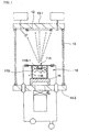
- FIG. 1 is a schematic sectional view showing the inner structure of a conventional apparatus for depositing an organic electroluminescent layer, and shows a deposition source 10 mounted in a vacuum chamber 13 of the deposition apparatus and a substrate 12 located above the deposition source 10 .
- the substrate 12 to be coated with the organic electroluminescent layers is mounted to an upper plate 13-1 of the chamber 13
- the deposition source 10 to have a deposition material 20 is mounted on a thermally insulating structure 14 fixed to a bottom wall 13-2 of the chamber 13.
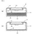
- FIG 2a is a sectional view showing the inner structure of the deposition source shown in FIG 1, and shows that a baffle 11B is provided in the deposition source 10 to prevent particulates or droplets contained in the vapor of the deposition material 20 from directly exiting through a vapor efflux aperture 11C formed on the top plate 11A of the deposition source 10.
- the baffle 11B corresponds to the vapor efflux aperture 11C and is fixed to a number of support rods 11B-1 fixed to the top plate 11A of the deposition source 10 to maintain certain space from the top plate 11A .
- the deposition apparatus using the deposition source 10 with the above structure has a heater or a heating means on (or under) the top plate 11A, or is constructed for the top plate 11A to have a heater in order to transfer heat to the deposition material 20 located around the center away from the side wall 11D .
- the heat generated at the side wall 11D as well as from the top plate 11A is transferred directly to the deposition material 20 so that the deposition material 20 is heated and vaporized.
- the vapor of vaporized deposition material 20 is moved along the surface of the baffle 11B and deposited on the substrate 12 (in FIG. 1) after exit through the vapor efflux aperture 11C .
- FIG. 2b is a sectional view showing the change of distance between the top plate of the deposition source in FIG. 1 and the deposition material after the deposition is processed for a certain amount of time.
- FIG. 2b shows a state that the distance between the top plate 11A and the surface of the deposition material 20 is increased.
- the quantity of the deposition material 20 received in the deposition source 10 is decreased gradually by heating and vaporizing reactions in progressing the deposition process also the thickness of the deposition material 20 is decreased.
- the initial distance (A in FIG. 2a) between the top plate 11A and the surface of the deposition material 20 in the deposition source is remarkably increased (a in FIG. 2b).
- the heat transfer path is increased so that the deposition rate (that is, vaporization rate of the deposition material) set at the initial stage is decreased.
- the temperature of the top plate 11A acting as the heater heating the deposition material 20 is needed.
- the distance between the top plate 11A and the surface of the deposition material 20 is increased. Under this situation, the sufficient heat generated at the top plate 11A cannot reach the deposition material 20 , and so the deposition material located on the center is not vaporized though the heat generated from the side wall 11D is supplied. Consequently, if the input amount of the deposition material 20 is high (that is, the thickness of the deposition material 20 is high), it is difficult to expect that all the deposition material is vaporized.
- the distance between the substrate 12 and the deposition material 20 which is directly related to the uniformity of deposition layer, is increased to result in change of the deposition characteristics in time.
- Low molecule organic electroluminescent material contains a large amount of organic material unstable to heat, and causes a problem of lowering the characteristics of the organic electroluminescent material by inducing resolution or change of the material characteristics due to excessive radiant heat in the deposition process.
- additional processes for cooling the chamber, exhausting the vacuum pressure, and re-vacuumizing are required to supply new deposition material to replenish the exhausted deposition material because the deposition process is conducted under high vacuum condition. Such additional processes cause loss of the process time.
- the initial deposition characteristics for example, vaporization rate of the deposition material
- the side wall 11D acts as a heating unit (for example, structure which coils are wound around the side wall 11D ).
- the thermal efficiency is lowered because all heat generated at the side wall 11D is not transferred to the deposition material 20 and some heat is radiated to the exterior.
- the deposition material 20 supplied in the deposition source 10 is consumed, and so the thickness of the deposition material 20 is decreased.
- heat is generated at the sidewall 11D corresponding to the portions without the deposition material and is not transferred directly to the deposition material, which contributes to energy waste.
- Another drawback of the deposition source 10 is that the heat generated at the top plate 11A and the side wall 11D is not sufficiently transferred to the deposition material 20 located at the lower portion of the deposition source 10 , that is, the deposition material 20 adjoining the surface of the bottom wall 11E . As a result, all of the deposition material 20 is not heated and vaporized. Particularly, depending on positions within the deposition source 10 , the temperature of each deposition material 20 becomes different, that is, thermal gradient within the deposition source. Therefore, it is difficult to form a uniform deposition layer on the substrate.
- An object of the present invention is to provide the deposition source which can compensate change of the distance between the heating means and the surface of the deposition material caused by decrease of the thickness of the deposition material according to consumption of the deposition material in the deposition process for the purpose of solving problems caused by increase of the distance between the top plate (heating means) of the deposition source and the surface of the deposition material supplied into the deposition source from the deposition process.
- Another object of the present invention is to provide the deposition source which can enhance thermal efficiency through preventing heat generated at the heating means from exiting to the exterior by adding a heat-cutting function.
- another object of the present invention is to provide the deposition source for forming organic electroluminescent layers which can obtain a uniform deposition layer by minimizing factors of temperature change and by efficiently using all the deposition material through supplying heat to the deposition source adjoining the surface of the bottom wall.
- the deposition source according to the present invention is installed in a chamber, heated by applied electric power to transfer heat to a vapor deposition material received therein and applying a vaporized deposition material generated therein to a substrate to form deposition organic electroluminescent layers onto the substrate, and comprises a vessel consisted of a top plate on which a vapor efflux aperture is formed, a side wall, and a bottom wall; a heating means for supplying heat to the deposition material received in the vessel, the heating means being capable of moving vertically; and a means for moving said heating means, the moving means being operated in response to the signal of a sensing means on varied distances between the heating means and the surface of said deposition material.
- the heating means is moved downward by the moving means to maintain the distance between the heating means and the surface of the deposition material at an initially-set value when the thickness of the deposition material is decreased.
- Another deposition source is installed in a chamber, to form deposition organic electroluminescent layers onto the substrate, by applying a vaporized deposition material generated therein to a substrate, by transferring heat to a vapor deposition material received therein, heated by applied electric power, and comprises a vessel consisted of a top plate on which a vapor efflux aperture is formed, a side wall, and a bottom plate, the bottom plate being capable of moving vertically; a heating means for supplying heat to the deposition material received in the vessel; and a means for moving said bottom plate, the moving means being operated in response to the signal of a sensing means on varied distances between the heating means and the surface of the deposition material.
- the bottom plate is moved upward by the moving means to maintain the distance between the heating means and the surface of the deposition material and the distance between the substrate to be coated and the surface of the deposition material at an initially-set value when the thickness of the deposition material is decreased.
- FIG. 3a is a sectional view of the deposition source according to the first embodiment of the present invention.
- a deposition source 100 according to the first embodiment is a vessel consisted of a top plate 101 , a side wall 102 , and a bottom wall 103 .
- the deposition source 100 contains solid organic electroluminescent vapor deposition material 20 (hereinafter, referred to as "deposition material").
- a vapor efflux aperture 101A is formed on the top plate 101 .
- the function of the vapor efflux aperture 101A is to discharge vapor of vaporized deposition material from the deposition source 100 .
- a baffle member 104 fixed to a lower surface of the top plate 101 corresponds to the efflux aperture 101A .
- the top plate 101 can act as a heating means (heater) for supplying heat to the deposition material 20 or a separate heating means can be placed on (or below) the top plate 101 .
- a heating means for supplying heat to the deposition material 20 or a separate heating means can be placed on (or below) the top plate 101 .
- a case where the top plate 101 acts as a heating means will be explained as an example.
- the most important feature of the first embodiment as shown in FIG. 3a is that the top plate 101 of the deposition source 100 can be vertically moved.
- a movement means 151 to move the top plate 101 is mounted to the top plate 101 .
- the movement means 151 used in the deposition source 100 is a hydraulic or pneumatic cylinder.
- Two support brackets 154 fixed a the side wall of the chamber ( 13 in FIG. 1) are extended above the deposition source 100 , and the cylinders 151 are mounted to each end portion of the brackets 154 .
- Rods 152 of each cylinder 151 are fixed to both sides of the top plates 101 , and therefore, each cylinder 151 does not have any effect on vapor efflux of the deposition material 20 through the aperture 101A of the top plate 101 .
- each cylinder 151 is controlled by a control means which is not shown in FIG. 3a, and the control means is connected to a sensing means 153 (for example, optical sensor) installed on the lower surface of the baffle 104 so that the control means can control each cylinder 151 according to a signal from the sensing means 153 .
- a sensing means 153 for example, optical sensor
- FIG. 3b is a detailed view showing part 3b in FIG. 3a.
- FIG. 3b shows partially the structure of the side wall 102 and the top plate 101 which can be vertically moved along the side wall 102 of the deposition source 100 .
- a number of vertical grooves 102-1 are formed on the inner surface of the side wall 102 , and protrusions 101-1 are formed on the outer circumference surface of the top plate 101.
- Each protrusion 101-1 corresponds to each groove 102-1 and can be received in the corresponding groove 102-1 when the top plate 101 and the side wall 102 are assembled.
- each protrusion 101-1 is moved along the corresponding groove 102-1. Consequently, the top plate 101 can be moved smoothly in the vertical direction without any deviation to the side wall 102 from the initial location.
- FIG. 3c is a view showing relationship between the top plate of the deposition source and the deposition material after the deposition process is completed. The function of the deposition source constructed as described above will be explained in reference to FIG. 3a and FIG. 3c.
- the quantity of the deposition material 20 received in the deposition source 100 is decreased gradually by the heating and vaporizing action.
- the distance between the surface of the deposition material 20 and the top plate 101 is changed (increased).
- the sensing means 153 mounted on the lower surface of the baffle 104 senses this change of the distance between the surface of the deposition material 20 and the top plate 101 , and then transmits the sensed signal to the control means.
- the control means calculates the distance between the surface of the deposition material 20 and the top plate 101 (that is, sum of the distance between the surface of the deposition material 20 and the sensing means 153, and the distance between the lower surface of the baffle 104 and the top plate 101 ) on the basis of the signals transmitted from the sensing means 153, and then compares the calculated distance with the initially-set distance (value).
- each cylinder 151 By operating each cylinder 151, the rods 152 of each cylinder 151 are extended downward so that the top plate 101 fixed to the ends of the rods 152 is moved downward along the side wall 102 .
- the control means halts the operation of each cylinder 151.
- the downward movement of the top plate 101 caused by the control means and each cylinder 151 is continued during the deposition process.
- the control means makes the rods 152 of each cylinder 151 return to the initial state as shown in FIG. 3a. Then, the top plate 101 of the deposition source 100 returns to its initial position, and thereafter, new deposition material is supplied to the deposition source 100.
- FIG. 3a and FIG. 3c show that the optical sensor 153 acting as the sensing means is installed on the lower surface of the baffle 104, but the optical sensor 153 can be installed at any position including the lower surface of the top plate 101 as long as the optical sensor 153 does not hinder the deposition process and can sense the distance between the surface of the deposition material 20 and the top plate 101 .
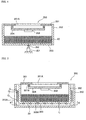
- FIG. 4 is a sectional view of the deposition source according to the second embodiment of the present invention.
- the entire structure of a deposition source 200 according to this embodiment is the same as that of the deposition source 100 shown in FIG. 3a and FIG. 3c.
- a top plate 201 can act as a heating means (heater) for supplying heat to the deposition material 20 or a separate heating means can be placed on (or below) the top plate 201 .
- a heating means herein, a separate heating means can be placed on (or below) the top plate 201 .
- a bottom plate 203 can be moved vertically in response to change of the distance between the surface of the deposition material 20 and the top plate 201 .
- the uniformity of the deposition layer to be formed on the surface of the substrate depends on change of the distance between the substrate 12 and the deposition material 20 .
- change of the distance between the top plate 101 and the deposition material 20 can be compensated by the vertical movement of the top plate 101 , but a means to adjust change of the distance between the substrate 12 and the deposition material 20 is not disclosed.
- the deposition source 200 has the structure which the bottom plate 203 can be moved vertically along a side wall 202 .
- a movement means 251 for moving the bottom plate 203 is mounted under the bottom plate 203 on which the deposition material 20 is located.
- the movement means used in the deposition source 200 according to the second embodiment is a hydraulic or pneumatic cylinder.
- the cylinder 251 is installed on a bottom wall 13-2 of the chamber 13 shown in FIG. 1, a rod 252 of the cylinder 251 is passed through the bottom wall 13-2, and the end of the rod 252 is fixed to the lower surface of the bottom plate 203 .
- the structure shown in FIG. 4 is merely an example, and so the cylinder having another structure can be installed.
- the cylinder 251 is controlled by a control means which is not shown in FIG. 4, the control means is connected to a sensing means 253 (for example, optical sensor) so that the control means controls the cylinder 251 according to the signal transmitted from the sensing means 253.
- a sensing means 253 for example, optical sensor
- a number of vertical grooves are formed on the inner surface of the side wall 202
- a number of protrusions are formed on the outer circumference surface of the bottom plate 203 .
- Each protrusion corresponds to each groove and can be received in the corresponding groove. Therefore, the bottom plate 203 can be moved smoothly in the vertical direction without any deviation to the side wall 202 from the initial location.
- This structure of the second embodiment is the same as that of the first embodiment as shown in FIG. 3c except difference of the member on which the protrusions are formed. Therefore, a further detailed description on the protrusions and grooves is omitted.
- the quantity of the deposition material 20 received in the deposition source 200 is decreased gradually by the heating and vaporizing actions.
- the distance between the substrate ( 12 in FIG. 1) and the deposition material 20 is increased (surely, the distance between the surface of the deposition material 20 and the top plate 201 is also increased, and the increased distance between the surface of the deposition material 20 and the top plate 201 is the same as the increased distance between the substrate 12 and the surface of the deposition material 20 ).
- the sensing means 253 mounted to a lower surface of a baffle 204 senses change of the distance between the surface of the deposition material 20 and the top plate 201 , and then transmits the sensed signal to the control means.
- the control means calculates the distance between the surface of the deposition material 20 and the top plate 201 on the basis of the signals transmitted from the sensing means 253 , and then compares the calculated distance with the initially-set distance.
- the control means operates the cylinder 251 installed under the bottom plate 203 .
- the rod 252 of the cylinder 251 is extended upward so that the bottom plate 203 fixed to the end of the rod 252 is moved upward along the side wall 202 .
- the control means halts the operation of the cylinder 251.
- the upward movement of the bottom plate 203 caused by the control means and the cylinder 251 is continued during the deposition process.
- the control means makes the rod 252 of the cylinder 251 return to the initial state.
- the bottom plate 203 of the deposition source 200 returns to its initial position, and thereafter, new deposition material is supplied to the deposition source 200 .
- FIG. 4 shows that the optical sensor 253 acting as the sensing means is installed at the lower surface of the baffle 204 , but the optical sensor can be installed at any positions including the lower surface of the top plate 201 as long as the optical sensor 253 does not hinder the deposition process and can sense the distance between the surface of the deposition material 20 and the top plate 201 .
- the distance between the surface of the deposition material 20 and the top plate 101 (the first embodiment) or the distance between the surface of the deposition material 20 and the substrate 12 (the second embodiment) can be maintained at the initially-set distance by the movement of the top plate 101 (the first embodiment) or the bottom plate 203 (the second embodiment).
- an appropriate amount of heat is transferred to the deposition material 20 during the deposition process so that the deposition temperature of the deposition material 2 0 can be maintained uniformly and the optimum deposition rate can be maintained.
- the distance between the top plate 201 and the deposition material 20 as well as the optimum distance between the substrate and the deposition material are always maintained, and so it is possible to form a uniform deposition layer.
- the deposition material adjoining the surface of the bottom plate 203 can be vaporized so that it is possible to minimize the residual of the deposition material.
- the second embodiment enables the depth of the deposition source to make deeper than the conventional depositional source, and so the quantity of the deposition material supplied to the deposition source can be maximized.
- FIG. 5 is a sectional view of the deposition source according to the third embodiment of the present invention.
- the deposition source 300 according to this embodiment has a vessel consisted of a top plate 301 acting as the heating means, a side wall 302 , and a bottom wall 303 .
- the structure of the top plate 301 , on which a vapor efflux aperture 301A is formed and to which a baffle member 304 is fixed, is the same as the top plates 101 and 201 of the deposition sources 100 and 200 of the first and second embodiments, respectively. Therefore, a further detailed description thereon is omitted.
- the important aspect of the deposition source 300 shown in FIG. 5 is that a number of coils C1, C2, ...Cn as a heating means for transferring heat to the deposition material 20 are wound around the side wall 302, and a casing 350 is located at the outer side of the side wall 302.
- a number of coils C1, C2, ...Cn are wound on the outer circumference surface of the side wall 302 .
- the uppermost coil C1 coincides with the surface of the deposition material 20 received in the deposition source with the maximum height (thickness), and the lowermost coil Cn coincides with the surface of the bottom wall 303 .
- the coils C1, C2, ...Cn are arranged for electric power to be individually applied thereto.
- a control means (not shown) controls the electric power applied to each coil C1 , C2, ...Cn, and the control means is connected to a sensing means 353 (for example, optical sensor) which is mounted to the interior of the deposition source.
- electric power is applied to only the uppermost coil C1 , not the other coils C2, ... Cn , by the control means.
- the upper side of the deposition material 20 is heated and vaporized by the heat generated at the top plate 301 acting as a heating means and by the heat generated at the uppermost coil C1 .
- the quantity of the deposition material 20 received in the deposition source 200 is decreased gradually by the heating and vaporizing action (that is, decrease of the height of the deposition material 20 ).
- the sensing means 353 mounted on the lower surface of the baffle 304 senses change of the height of the deposition material 20 , and transmits the sensed signal to the control means. Then, the control means calculates the height of the deposition material 20 on the basis of the signals transmitted from the sensing means 353 . According to the calculated height of the deposition material 20 , the control means controls the electric power applied to the other coils C1, C2, ...Cn .
- the control means blocks the electric power applied to the uppermost coil C1 and applies the electric power to the second coil C2.
- control means applies the electric power to the lowermost coil Cn and blocks the electric power applied to the other coils C1, C2 ...
- any one coil to which the electric power is applied always corresponds to a portion of the deposition material 20 to which the heat generated by the top plate 301 is transferred. Therefore, it is possible to prevent the heat generated by the coils C1 , C2, ... Cn from transferring unnecessarily to the portion of the deposition material which heating and vaporizing do not take place and the deposition material is not present.
- the casing 350 located at the outer side of the side wall 302 prevents the heat generated at each coil C1, C2, ...Cn from radiating outward.
- most of the heat generated at each coil C1, C2, ...Cn is transferred to the deposition material 20 through the side wall 302 so that it is possible to minimize heat loss.
- the space formed between the side wall 302 and the outer casing 350 is filled with a thermal insulation material, the heat radiation is prevented more effectively to minimize thermal gradient in the entire system.
- the reference numeral 350A indicates the opening formed on the casing 350 for connecting power lines to the coils C1, C2, ...Cn .
- More excellent adiabatic property can be obtained by forming the casing 350 with oxide or nitride of aluminum (Al), zirconium (Zr), silicon (Si), yttrium (Y), etc., having high thermal capacity.
- FIG. 6 is a sectional view taken along the line 6-6 in FIG. 5 and shows a recess 303A formed at the lower surface of the bottom wall 303 and a coil C received in the recess 303A .
- the recess 303A is formed to the longitudinal (or widthwise) direction on the bottom wall 303 , and consists of many linear portions and connection portions connecting two neighboring linear portions.
- the single coil C is spread on the entire surface of the bottom wall 303 . Both ends of the coil C are connected to the power supply (not shown).
- the electric power is applied to any one of the coils C1, C2, ...Cn wound around the side wall 302 as well as the coil C received in the recess 303 A of the bottom wall 303 (surely, the electric power is applied to the top plate 301 acting as a heating means). Therefore, the heat generated at the coil C received in the recess 303A of the bottom wall 303 is transferred to the deposition material adjoining the surface of the bottom wall 303 .
- the coil to which the electric power is applied is always corresponded to a portion of the deposition material to which heat generated by the top plate is transferred. Therefore, it is possible to prevent heat generated by the coils from transferring unnecessarily to a portion of the deposition material which is not heated and vaporized and a portion of the deposition source in which the deposition material is not present.
- the casing provided at the exterior of the side wall prevents the heat generated at the coils mounted to the side wall from radiating outward, and so most generated heat is transferred to the deposition material through the side wall to minimize thermal gradient in the entire system.
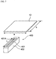
- FIG. 7 is a schematic perspective view showing relationship between the deposition source according to the fourth embodiment and the substrate. An inner structure of the deposition source 400 is not shown in FIG. 7.
- the deposition source 400 is consisted of a top plate 401 with certain length and width, a side wall 402 , and a bottom wall.
- a vapor efflux aperture 401A is formed on the top plate 401 .
- An organic electroluminescent vapor deposition material is received in the space formed by the top plate 401, the side wall 402, and the bottom wall.
- a feature of this embodiment is to constitute the deposition source 400 whose effective deposition length (that is, length A of the vapor efflux aperture 401A of the top plate 401 actually contributing to the deposition process) is longer than, or the same as, the width b of the substrate 12 on which the electroluminescent layer is formed.
- FIG. 8a is a plane view of the substrate showing the initial state that the electroluminescent layer is formed on the surface of the substrate by means of the deposition source 400 shown in FIG. 7. If the deposition source 400 as described above is used for forming the electroluminescent layer on the surface of the substrate 12, the deposition material's vapor is diffused through the aperture 400A of the top plate 401 , and then dispersed and deposited uniformly on the surface of the substrate 12 over the entire width.
- the more effective deposition process can be performed by moving the deposition source 400 constructed as described above or the substrate 20 to the longitudinal direction of the substrate. That is, when the deposition source 400 or the substrate 20 is moved horizontally (linearly) to the arrow direction shown in FIG. 8, the electroluminescent layer as shown in FIG. 8a is continuously deposited on the surface of the substrate 12 over the entire length. Ultimately, as shown in FIG. 8b showing the surface of the substrate on which the deposition of the electroluminescent layer is completed after moving horizontally the deposition source 400 or the substrate 12 , the uniform electroluminescent layer is formed on the entire surface of the substrate 12 .
- each respective deposition source 100 , 200 , 300 and 400 described in the first to fourth embodiments has the inner space divided into the lower and upper portion, and the cross sectional surface of the lower portion is the same as that of the upper portion. Therefore, the flow rate of vapor of the deposition material at the lower portion is practically equal to the flow rate at the upper portion. Also, due to the large surface area of the upper portion of the deposition source, heat loss of the deposition material in the inner space is increased. In order to eliminate the above drawbacks, the present invention modified the shape of the deposition source.
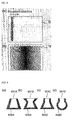
- FIG. 9a to FIG. 9d are sectional views of the deposition sources, and show various shapes of the deposition source according to the present invention. Another feature of the deposition sources 500A , 500B , 500C , and 500D according to the present invention is that the sectional surface area of the upper portion at which the aperture is formed is smaller than that of the lower portion.
- sectional surface areas in a tube can be different in different positions, the quantity of flow is same anywhere in the tube, and therefore, the flow rate of a portion having smaller sectional surface area is higher than that of another portion having larger sectional surface area.
- the flow rate of vapor at the upper portion having smaller sectional surface area is higher than that of vapor at the lower portion of the deposition source.
- Higher flow rate induces increase of the vapor's kinetic energy (molecules of the vaporized deposition material), and so the density and uniformity of the deposition layer formed on the substrate can be enhanced.
- the sectional surface area of the upper portion through which the vapor of the deposition material is diffused is small, heat loss outward can be minimized and the deposition source is not influenced by such exterior interference as change of ambient temperature.
- a material having higher thermal capacity than quartz for example, oxide or nitride of aluminum (Al), zirconium (Zr), silicon (Si), or yttrium (Y), or composite material of at least two above, is used as the deposition source's material.
- the thermal capacity of these metal oxide or nitride is larger than organic material used as the deposition material (about 3:1), and therefore, the adiabatic property of the deposition source can be improved.
Landscapes
- Chemical & Material Sciences (AREA)
- Engineering & Computer Science (AREA)
- Chemical Kinetics & Catalysis (AREA)
- Materials Engineering (AREA)
- Mechanical Engineering (AREA)
- Metallurgy (AREA)
- Organic Chemistry (AREA)
- Manufacturing & Machinery (AREA)
- Physical Vapour Deposition (AREA)
- Electroluminescent Light Sources (AREA)
Abstract
Description
Claims (23)
- A deposition source installed in a chamber, heated by applied electric power to transfer heat to a vapor deposition material received therein and applying a vaporized deposition material generated therein to a substrate to form deposition organic electroluminescent layers onto the substrate, comprising;a vessel consisted of a top plate on which a vapor efflux aperture is formed, a side wall, and a bottom wall;a heating means for supplying heat to the deposition material received in said vessel, said heating means being capable of moving vertically; anda means for moving said heating means, said moving means being operated in response to the signal of a sensing means on varied distances between said heating means and the surface of said deposition material, whereby said heating means is moved downward by said moving means to maintain the distance between said heating means and the surface of the deposition material at an initially-set value when the thickness of the deposition material is decreased.
- The deposition source according to claim 1, wherein said sensing means and said heating means are mounted to said top plate, said moving means comprises a number of cylinders supported by said chamber and for moving said top plate vertically with having rods fixed to said top plate; and a control means receiving a signal from said sensing means and controlling said cylinders in response to the transmitted signal, whereby said cylinders make said top plate move downward along said side wall when the distance between said top plate and said deposition material is larger than the initially-set value.
- The deposition source according to claim 2, wherein each of said cylinders is installed at the outer side which does not correspond to said vapor efflux aperture formed on said top plate so that each of said cylinders does not affect the flow of vapor of said deposition material escaped through said vapor efflux aperture.
- The deposition source according to at least one of the preceding claims, wherein said side wall has a number of vertical grooves formed on the inner surface thereof, and said top plate has a number of protrusions formed on the outer circumference surface thereof, each of said protrusions has such a size that each protrusion can be received in each of said grooves that each of said protrusions of said top plate is moved along each of said grooves of said side wall when said top plate is moved vertically.
- A deposition source installed in a chamber, to form deposition organic electroluminescent layers onto the substrate, by applying a vaporized deposition material generated therein to a substrate, by transferring heat to a vapor deposition material received therein, heated by applied electric power, comprising;a vessel consisted of a top plate on which a vapor efflux aperture is formed, a side wall, and a bottom plate, said bottom plate being capable of moving vertically;a heating means for supplying heat to said deposition material received in said vessel; anda means for moving said bottom plate, said moving means being operated in response to the signal of a sensing means on varied distances between said heating means and the surface of said deposition material, whereby said bottom plate is moved upward by said moving means to maintain the distance between said heating means and the surface of the deposition material and the distance between said substrate to be coated and the surface of the deposition material at an initially-set value when the thickness of the deposition material is decreased.
- The deposition source according to claim 5, wherein said moving means comprisesa cylinder supported by said chamber and for moving vertically said bottom plate with having a rod fixed to said bottom plate; anda control means receiving a signal transmitted from said sensing means mounted to said top plate and controlling said cylinder in response to the transmitted signal, whereby said cylinder makes said bottom plate move upward along said side wall when the distance between said heating means and the surface of said deposition material is larger than the initially-set value.
- The deposition source according to claim 5 or 6, wherein said side wall has a number of vertical grooves formed on the inner surface thereof, and said bottom plate has a number of protrusions formed on the outer circumference surface thereof, each of said protrusions has such a size that each protrusion can be received in each of said grooves so that each of said protrusions of said bottom plate is moved along each of said grooves of said side wall when said bottom plate is moved vertically.
- The deposition source according to at least one of claims 5 to 7, wherein said sensing means is an optical sensor.
- A deposition source installed in a chamber, to form deposition organic electroluminescent layers onto a substrate, by applying a vaporized deposition material generated therein to the substrate, and by transferring heat to a vapor deposition material received therein, heated by applied electric power, comprising; a top plate on which a vapor efflux aperture is formed, a side wall, a bottom plate, a heating means for supplying heat to the deposition material corresponding to a certain position, a sensing means for sensing change of the height of the deposition material, and a controlling means for controlling said heating means selectively in response to a signal of said sensing means.
- The deposition source according to claim 9, wherein said heating means is a number of coils wound on the outer circumference surface of said side wall so that electric power is applied to each coil by controlling said controlling means according to the height of the deposition material.
- The deposition source according to claim 10, wherein the uppermost coil of said coils coincides with the surface of said deposition material received at the maximum height and the lowermost coil coincides with the surface of said bottom wall.
- The deposition source according to claim 10 or 11, wherein said controlling means controls said coils by applying electric power to only the coil adjacent to the surface of said deposition material when the height of the deposition material is changed during the deposition process.
- The deposition source according to at least one of claims 9 to 12, wherein said bottom wall has a groove formed on the lower surface thereof and a coil is received in said groove so that the heat generated at said coil is transferred to the deposition material adjoining the surface of said bottom wall when electric power is applied to said coil.
- The deposition source according to claim 13, wherein said groove formed on said bottom wall is in the direction of width or length of said bottom wall, and is consisted of a number of linear portions and connection portions connecting two neighboring linear portions, whereby said groove is formed on the entire surface of said bottom wall.
- The deposition source according to at least one of claims 9 to 14, wherein said deposition source further comprises a casing provided at the outer portion of said side wall for preventing heat generated at said heating means from transferring to the exterior.
- The deposition source according to claim 15, wherein the space between said side wall and said casing is filled with a thermal insulation material.
- The deposition source according to claim 15 or 16, wherein said casing is made of oxide or nitride of aluminum (Al), zirconium (Zr), silicon (Sr), or yttrium (Y).
- A deposition source installed in a chamber, to form deposition organic electroluminescent layers onto a substrate, by applying a vaporized deposition material generated therein to the substrate, and by transferring heat to a vapor deposition material received therein, heated by applied electric power, comprising; a top plate on which a vapor efflux aperture is formed, a side wall, and a bottom plate, said vapor efflux aperture having a length which is longer than, or the same as, the width of said substrate to be coated with a deposition organic electroluminescent layers.
- The deposition source according to claim 18, wherein said deposition source is capable of moving to the horizontal direction with respect to said substrate.
- The deposition source according to claim 18 or 19, wherein said substrate is capable of moving to the horizontal direction with respect to said deposition source.
- The deposition source according to at least one of claims 18 to 20, wherein said deposition source has the upper portion and the lower portion, said upper portion has a sectional surface area smaller than that said lower portion.
- The deposition source according to at least one of claims 18 to 21, wherein said deposition source is made from a material having thermal capacity which is higher than said deposition material.
- The deposition source according to at least one of claims 18 to 22, wherein said deposition source is made of oxide or nitride of aluminum (Al), zirconium (Zr), silicon (Si), or yttrium (Y), or composite material of at least two above.
Priority Applications (2)
| Application Number | Priority Date | Filing Date | Title |
|---|---|---|---|
| EP05003605.2A EP1560467B1 (en) | 2002-07-19 | 2003-07-18 | Source for thermal physical vapor deposition of organic electroluminescent layers |
| EP05003606.0A EP1560468B1 (en) | 2002-07-19 | 2003-07-18 | Source for thermal physical vapor deposition of organic electroluminescent layers |
Applications Claiming Priority (6)
| Application Number | Priority Date | Filing Date | Title |
|---|---|---|---|
| KR10-2002-0042271A KR100471358B1 (en) | 2002-07-19 | 2002-07-19 | Device for depositing electroluminescent layer |
| KR2002042271 | 2002-07-19 | ||
| KR2002058116 | 2002-09-25 | ||
| KR10-2002-0058116A KR100471361B1 (en) | 2002-09-25 | 2002-09-25 | Apparatus for depositing organic- electroluminescent device |
| KR1020020059786A KR100669194B1 (en) | 2002-10-01 | 2002-10-01 | Organic Electroluminescent Element Evaporation Source |
| KR2002059786 | 2002-10-01 |
Related Child Applications (2)
| Application Number | Title | Priority Date | Filing Date |
|---|---|---|---|
| EP05003606.0A Division EP1560468B1 (en) | 2002-07-19 | 2003-07-18 | Source for thermal physical vapor deposition of organic electroluminescent layers |
| EP05003605.2A Division EP1560467B1 (en) | 2002-07-19 | 2003-07-18 | Source for thermal physical vapor deposition of organic electroluminescent layers |
Publications (3)
| Publication Number | Publication Date |
|---|---|
| EP1382713A2 true EP1382713A2 (en) | 2004-01-21 |
| EP1382713A3 EP1382713A3 (en) | 2004-06-02 |
| EP1382713B1 EP1382713B1 (en) | 2006-05-17 |
Family
ID=36571445
Family Applications (3)
| Application Number | Title | Priority Date | Filing Date |
|---|---|---|---|
| EP05003606.0A Expired - Lifetime EP1560468B1 (en) | 2002-07-19 | 2003-07-18 | Source for thermal physical vapor deposition of organic electroluminescent layers |
| EP05003605.2A Expired - Lifetime EP1560467B1 (en) | 2002-07-19 | 2003-07-18 | Source for thermal physical vapor deposition of organic electroluminescent layers |
| EP03016305A Expired - Lifetime EP1382713B1 (en) | 2002-07-19 | 2003-07-18 | Source for thermal physical vapour deposition of organic electroluminescent layers |
Family Applications Before (2)
| Application Number | Title | Priority Date | Filing Date |
|---|---|---|---|
| EP05003606.0A Expired - Lifetime EP1560468B1 (en) | 2002-07-19 | 2003-07-18 | Source for thermal physical vapor deposition of organic electroluminescent layers |
| EP05003605.2A Expired - Lifetime EP1560467B1 (en) | 2002-07-19 | 2003-07-18 | Source for thermal physical vapor deposition of organic electroluminescent layers |
Country Status (6)
| Country | Link |
|---|---|
| US (3) | US7025832B2 (en) |
| EP (3) | EP1560468B1 (en) |
| JP (3) | JP3924751B2 (en) |
| CN (1) | CN1226448C (en) |
| AT (1) | ATE326555T1 (en) |
| DE (1) | DE60305246T2 (en) |
Cited By (5)
| Publication number | Priority date | Publication date | Assignee | Title |
|---|---|---|---|---|
| EP1443127A1 (en) * | 2003-01-28 | 2004-08-04 | Eastman Kodak Company | Method for coating large-area substrates |
| WO2005083145A3 (en) * | 2004-02-25 | 2006-02-02 | Eastman Kodak Co | Vapor deposition source with minimized condensation effects |
| CN101041891B (en) * | 2006-03-22 | 2010-04-21 | 佳能株式会社 | Vapor deposition source and vapor deposition apparatus |
| EP1918413A4 (en) * | 2005-08-25 | 2010-06-02 | Tokki Kk | METHOD FOR VACUUM DEPOSITION OF ORGANIC MATERIAL AND CORRESPONDING APPARATUS |
| EP2682503A1 (en) * | 2012-07-04 | 2014-01-08 | Riber | Evaporation device for a vacuum-deposition apparatus and vacuum-deposition apparatus including such an evaporation device |
Families Citing this family (41)
| Publication number | Priority date | Publication date | Assignee | Title |
|---|---|---|---|---|
| US7232588B2 (en) * | 2004-02-23 | 2007-06-19 | Eastman Kodak Company | Device and method for vaporizing temperature sensitive materials |
| US20060099344A1 (en) * | 2004-11-09 | 2006-05-11 | Eastman Kodak Company | Controlling the vaporization of organic material |
| US7399422B2 (en) * | 2005-11-29 | 2008-07-15 | Asml Holding N.V. | System and method for forming nanodisks used in imprint lithography and nanodisk and memory disk formed thereby |
| ATE471997T1 (en) * | 2005-05-31 | 2010-07-15 | Corus Technology Bv | DEVICE AND METHOD FOR COATING A SUBSTRATE |
| DE102005049906B4 (en) * | 2005-10-17 | 2009-12-03 | Von Ardenne Anlagentechnik Gmbh | Method and apparatus for evaporating evaporation material |
| US20070178225A1 (en) * | 2005-12-14 | 2007-08-02 | Keiji Takanosu | Vapor deposition crucible, thin-film forming apparatus comprising the same, and method of producing display device |
| JP2007291506A (en) * | 2006-03-31 | 2007-11-08 | Canon Inc | Deposition method |
| KR101106289B1 (en) * | 2006-08-04 | 2012-01-18 | 순천향대학교 산학협력단 | Linear Deposition Sources for Deposition Processes |
| WO2008045972A2 (en) * | 2006-10-10 | 2008-04-17 | Asm America, Inc. | Precursor delivery system |
| DE102008016619B3 (en) | 2008-04-01 | 2009-11-05 | Kennametal Sintec Keramik Gmbh | evaporator body |
| KR101196564B1 (en) * | 2008-04-11 | 2012-11-01 | 도시바 미쓰비시덴키 산교시스템 가부시키가이샤 | Heat equalizer |
| US20100189929A1 (en) * | 2009-01-28 | 2010-07-29 | Neal James W | Coating device and deposition apparatus |
| JP5421619B2 (en) | 2009-03-06 | 2014-02-19 | レオン自動機株式会社 | Method and apparatus for folding and loading food dough |
| US20120006809A1 (en) * | 2010-06-23 | 2012-01-12 | Colorado State University Research Foundation | Sublimation crucible with embedded heater element |
| TW201200614A (en) * | 2010-06-29 | 2012-01-01 | Hon Hai Prec Ind Co Ltd | Coating device |
| CN102312200B (en) * | 2010-06-30 | 2014-04-23 | 鸿富锦精密工业(深圳)有限公司 | Evaporator |
| JP5557633B2 (en) * | 2010-07-15 | 2014-07-23 | 日立造船株式会社 | Vapor deposition equipment |
| JP5674431B2 (en) * | 2010-11-17 | 2015-02-25 | 株式会社アルバック | Thin film forming equipment |
| CN102485952B (en) * | 2010-12-06 | 2015-09-23 | 理想能源设备有限公司 | Vapourizing unit and gasification method |
| JP2012132049A (en) * | 2010-12-20 | 2012-07-12 | Mitsubishi Heavy Ind Ltd | Vacuum deposition device and vacuum deposition method |
| DE102010055285A1 (en) * | 2010-12-21 | 2012-06-21 | Solarion Ag Photovoltaik | Evaporator source, evaporator chamber and coating process |
| KR101233629B1 (en) * | 2011-04-13 | 2013-02-15 | 에스엔유 프리시젼 주식회사 | Large capacity depositing apparatus for forming thin film |
| KR101052435B1 (en) * | 2011-04-13 | 2011-07-28 | 에스엔유 프리시젼 주식회사 | Thin film deposition equipment |
| KR20120116720A (en) * | 2011-04-13 | 2012-10-23 | 에스엔유 프리시젼 주식회사 | Apparatus for supplying materials |
| KR101252756B1 (en) * | 2011-08-08 | 2013-04-09 | 공주대학교 산학협력단 | Nozzle of point source |
| MX349646B (en) * | 2012-06-08 | 2017-08-04 | Univ Houston | Self-cleaning coatings and methods for making same. |
| KR101433901B1 (en) | 2012-10-25 | 2014-09-01 | 지제이엠 주식회사 | Apparatus and method for the deposition of the organic materials |
| CN104099571A (en) * | 2013-04-01 | 2014-10-15 | 上海和辉光电有限公司 | Evaporation source component, film deposition device and film deposition method |
| KR102098619B1 (en) * | 2013-05-31 | 2020-05-25 | 삼성디스플레이 주식회사 | Cubicle apparatus and deposition apparatus with the same |
| CN105177510B (en) * | 2015-10-21 | 2018-04-03 | 京东方科技集团股份有限公司 | Evaporated device and evaporation coating method |
| US11926894B2 (en) | 2016-09-30 | 2024-03-12 | Asm Ip Holding B.V. | Reactant vaporizer and related systems and methods |
| US10876205B2 (en) | 2016-09-30 | 2020-12-29 | Asm Ip Holding B.V. | Reactant vaporizer and related systems and methods |
| CN106906445B (en) * | 2017-03-29 | 2019-02-12 | 武汉华星光电技术有限公司 | A kind of evaporation source |
| CN107805782B (en) * | 2017-11-27 | 2019-09-20 | 深圳市华星光电半导体显示技术有限公司 | A kind of evaporation coating device |
| WO2019239192A1 (en) * | 2018-06-15 | 2019-12-19 | Arcelormittal | Vacuum deposition facility and method for coating a substrate |
| US11634812B2 (en) | 2018-08-16 | 2023-04-25 | Asm Ip Holding B.V. | Solid source sublimator |
| DE102018131905B4 (en) * | 2018-12-12 | 2024-04-25 | VON ARDENNE Asset GmbH & Co. KG | Evaporation arrangement and method |
| KR102221960B1 (en) * | 2019-03-25 | 2021-03-04 | 엘지전자 주식회사 | Deposition apparatus |
| JP7303031B2 (en) * | 2019-06-07 | 2023-07-04 | 株式会社アルバック | Evaporation source for vacuum deposition equipment |
| CN110344004A (en) * | 2019-08-29 | 2019-10-18 | 上海天马有机发光显示技术有限公司 | A kind of vapor deposition crucible and evaporated device |
| US11624113B2 (en) | 2019-09-13 | 2023-04-11 | Asm Ip Holding B.V. | Heating zone separation for reactant evaporation system |
Family Cites Families (58)
| Publication number | Priority date | Publication date | Assignee | Title |
|---|---|---|---|---|
| US1556930A (en) * | 1924-07-15 | 1925-10-13 | Grau Hans | Electrical heater |
| US2440135A (en) | 1944-08-04 | 1948-04-20 | Alexander Paul | Method of and apparatus for depositing substances by thermal evaporation in vacuum chambers |
| US2793609A (en) * | 1953-01-26 | 1957-05-28 | British Dielectric Res Ltd | Means for the deposition of materials by evaporation in a vacuum |
| US2955190A (en) * | 1957-07-01 | 1960-10-04 | Ferro Corp | Circuitous resistance plate type electric heater |
| US3904392A (en) * | 1973-03-16 | 1975-09-09 | Eastman Kodak Co | Method of and apparatus for debubbling liquids |
| US3971334A (en) * | 1975-03-04 | 1976-07-27 | Xerox Corporation | Coating device |
| JPS56108286A (en) * | 1979-11-01 | 1981-08-27 | Xerox Corp | Method of manufacturing photoreceptor |
| US4440803A (en) * | 1979-11-01 | 1984-04-03 | Xerox Corporation | Process for preparing arsenic-selenium photoreceptors |
| JPS59107075A (en) * | 1982-12-13 | 1984-06-21 | Mitsubishi Heavy Ind Ltd | Controlling method of evaporation rate |
| JPS6026660A (en) * | 1983-07-26 | 1985-02-09 | Ulvac Corp | Control device for melt surface of source of evaporation |
| JPS60181267A (en) * | 1984-02-28 | 1985-09-14 | Mitsubishi Electric Corp | Apparatus for melting metal |
| JPS6086270A (en) * | 1984-06-01 | 1985-05-15 | Denki Kagaku Kogyo Kk | Preparation of resistance heater |
| JPH0238559B2 (en) * | 1984-11-16 | 1990-08-30 | Hitachi Ltd | BUNSHISENJOCHAKUSOCHI |
| US4695316A (en) * | 1986-06-27 | 1987-09-22 | Inductotherm Corporation | Multiple induction furnace system using single power supply |
| JPS6314861A (en) * | 1986-07-08 | 1988-01-22 | Nippon Kokan Kk <Nkk> | Vacuum deposition equipment |
| JPH02122068A (en) * | 1988-10-31 | 1990-05-09 | Kawasaki Steel Corp | Method and device for supplying vaporization material in dry plating |
| US4914275A (en) * | 1988-11-08 | 1990-04-03 | Northern Indiana Public Service Company | Regasifier |
| JPH03134159A (en) * | 1989-10-19 | 1991-06-07 | Matsushita Electric Ind Co Ltd | vacuum evaporation source |
| JPH05139882A (en) * | 1991-11-20 | 1993-06-08 | Hitachi Ltd | Molecular beam source |
| JPH05182196A (en) * | 1991-12-27 | 1993-07-23 | Sony Corp | Thin film forming method and apparatus and vacuum evaporation crucible |
| JPH0572965U (en) * | 1992-03-11 | 1993-10-05 | 住友電気工業株式会社 | Crucible |
| JPH06228740A (en) * | 1993-01-29 | 1994-08-16 | Sony Corp | Vacuum deposition device |
| JPH0770739A (en) * | 1993-09-07 | 1995-03-14 | Mitsubishi Heavy Ind Ltd | Temperature control device for crucible for vapor deposition |
| US5803976A (en) * | 1993-11-09 | 1998-09-08 | Imperial Chemical Industries Plc | Vacuum web coating |
| JPH07268613A (en) * | 1994-03-31 | 1995-10-17 | Eiko Eng:Kk | Molecular-beam cell |
| DE4422697C1 (en) | 1994-06-29 | 1996-01-25 | Zsw | Vapour coating device for prodn. of thin filmed solar cells |
| US5532102A (en) * | 1995-03-30 | 1996-07-02 | Xerox Corporation | Apparatus and process for preparation of migration imaging members |
| DE19605335C1 (en) * | 1996-02-14 | 1997-04-03 | Fraunhofer Ges Forschung | Controlling a vacuum coating process |
| EP0826434B1 (en) * | 1996-07-31 | 2004-06-16 | Istituto Nazionale Di Fisica Nucleare | Process and apparatus for preparing thin films of polymers and composite materials on different kind of substrates |
| JPH10124869A (en) * | 1996-10-14 | 1998-05-15 | Fuji Photo Film Co Ltd | Device for producing magnetic recording medium |
| US6173609B1 (en) * | 1997-06-20 | 2001-01-16 | Optical Sensor Consultants, Inc. | Optical level sensor |
| CA2237534A1 (en) * | 1997-06-23 | 1998-12-23 | P.A. Joel Smith | Rod-fed source pool height monitor |
| JPH1161386A (en) * | 1997-08-22 | 1999-03-05 | Fuji Electric Co Ltd | Organic thin film light emitting device |
| US20030164225A1 (en) * | 1998-04-20 | 2003-09-04 | Tadashi Sawayama | Processing apparatus, exhaust processing process and plasma processing |
| JP2000012218A (en) | 1998-06-23 | 2000-01-14 | Tdk Corp | Apparatus and method for manufacturing organic EL element |
| US6251233B1 (en) * | 1998-08-03 | 2001-06-26 | The Coca-Cola Company | Plasma-enhanced vacuum vapor deposition system including systems for evaporation of a solid, producing an electric arc discharge and measuring ionization and evaporation |
| JP2000138095A (en) * | 1998-08-26 | 2000-05-16 | Toray Ind Inc | Light emitting device manufacturing method |
| US6202591B1 (en) * | 1998-11-12 | 2001-03-20 | Flex Products, Inc. | Linear aperture deposition apparatus and coating process |
| JP2000248358A (en) * | 1999-03-01 | 2000-09-12 | Casio Comput Co Ltd | Evaporation apparatus and evaporation method |
| JP3095740B2 (en) * | 1999-05-19 | 2000-10-10 | 福島県 | Evaporator for organic compounds |
| US6464795B1 (en) * | 1999-05-21 | 2002-10-15 | Applied Materials, Inc. | Substrate support member for a processing chamber |
| JP2001052862A (en) * | 1999-08-04 | 2001-02-23 | Hokuriku Electric Ind Co Ltd | Manufacture of organic el element and device therefor |
| JP2001057289A (en) * | 1999-08-20 | 2001-02-27 | Tdk Corp | Manufacturing device for organic el display device and manufacture thereof |
| JP4187367B2 (en) * | 1999-09-28 | 2008-11-26 | 三洋電機株式会社 | ORGANIC LIGHT EMITTING ELEMENT, ITS MANUFACTURING DEVICE, AND ITS MANUFACTURING METHOD |
| TW490714B (en) | 1999-12-27 | 2002-06-11 | Semiconductor Energy Lab | Film formation apparatus and method for forming a film |
| US6237529B1 (en) * | 2000-03-03 | 2001-05-29 | Eastman Kodak Company | Source for thermal physical vapor deposition of organic electroluminescent layers |
| JP4785269B2 (en) * | 2000-05-02 | 2011-10-05 | 株式会社半導体エネルギー研究所 | Manufacturing method of light emitting device and cleaning method of film forming device |
| EP1167566B1 (en) * | 2000-06-22 | 2011-01-26 | Panasonic Electric Works Co., Ltd. | Apparatus for and method of vacuum vapor deposition |
| JP3497450B2 (en) * | 2000-07-06 | 2004-02-16 | 東京エレクトロン株式会社 | Batch heat treatment apparatus and control method thereof |
| JP2002175878A (en) * | 2000-09-28 | 2002-06-21 | Sanyo Electric Co Ltd | Layer forming method and color light emitting device manufacturing method |
| US20030015140A1 (en) * | 2001-04-26 | 2003-01-23 | Eastman Kodak Company | Physical vapor deposition of organic layers using tubular sources for making organic light-emitting devices |
| JP4704605B2 (en) * | 2001-05-23 | 2011-06-15 | 淳二 城戸 | Continuous vapor deposition apparatus, vapor deposition apparatus and vapor deposition method |
| JP2003002778A (en) * | 2001-06-26 | 2003-01-08 | International Manufacturing & Engineering Services Co Ltd | Molecular beam cell for thin film deposition |
| JP3712646B2 (en) * | 2001-08-03 | 2005-11-02 | 株式会社エイコー・エンジニアリング | Molecular beam cell for thin film deposition |
| US20030101937A1 (en) * | 2001-11-28 | 2003-06-05 | Eastman Kodak Company | Thermal physical vapor deposition source for making an organic light-emitting device |
| US20030168013A1 (en) * | 2002-03-08 | 2003-09-11 | Eastman Kodak Company | Elongated thermal physical vapor deposition source with plural apertures for making an organic light-emitting device |
| US20040007183A1 (en) * | 2002-07-11 | 2004-01-15 | Ulvac, Inc. | Apparatus and method for the formation of thin films |
| US6837939B1 (en) * | 2003-07-22 | 2005-01-04 | Eastman Kodak Company | Thermal physical vapor deposition source using pellets of organic material for making OLED displays |
-
2003
- 2003-07-18 EP EP05003606.0A patent/EP1560468B1/en not_active Expired - Lifetime
- 2003-07-18 EP EP05003605.2A patent/EP1560467B1/en not_active Expired - Lifetime
- 2003-07-18 EP EP03016305A patent/EP1382713B1/en not_active Expired - Lifetime
- 2003-07-18 US US10/621,471 patent/US7025832B2/en not_active Expired - Lifetime
- 2003-07-18 AT AT03016305T patent/ATE326555T1/en not_active IP Right Cessation
- 2003-07-18 CN CNB031787649A patent/CN1226448C/en not_active Expired - Lifetime
- 2003-07-18 DE DE60305246T patent/DE60305246T2/en not_active Expired - Lifetime
- 2003-07-22 JP JP2003277602A patent/JP3924751B2/en not_active Expired - Lifetime
-
2005
- 2005-11-04 US US11/266,366 patent/US20060070576A1/en not_active Abandoned
- 2005-11-04 US US11/266,365 patent/US7815737B2/en not_active Expired - Lifetime
-
2006
- 2006-12-20 JP JP2006343450A patent/JP4429305B2/en not_active Expired - Lifetime
- 2006-12-20 JP JP2006343506A patent/JP2007123285A/en active Pending
Cited By (7)
| Publication number | Priority date | Publication date | Assignee | Title |
|---|---|---|---|---|
| EP1443127A1 (en) * | 2003-01-28 | 2004-08-04 | Eastman Kodak Company | Method for coating large-area substrates |
| WO2005083145A3 (en) * | 2004-02-25 | 2006-02-02 | Eastman Kodak Co | Vapor deposition source with minimized condensation effects |
| EP1918413A4 (en) * | 2005-08-25 | 2010-06-02 | Tokki Kk | METHOD FOR VACUUM DEPOSITION OF ORGANIC MATERIAL AND CORRESPONDING APPARATUS |
| US8357241B2 (en) | 2005-08-25 | 2013-01-22 | Canon Tokki Corporation | Method of organic material vacuum evaporation and apparatus thereof |
| CN101041891B (en) * | 2006-03-22 | 2010-04-21 | 佳能株式会社 | Vapor deposition source and vapor deposition apparatus |
| EP2682503A1 (en) * | 2012-07-04 | 2014-01-08 | Riber | Evaporation device for a vacuum-deposition apparatus and vacuum-deposition apparatus including such an evaporation device |
| FR2992976A1 (en) * | 2012-07-04 | 2014-01-10 | Riber | EVAPORATION DEVICE FOR VACUUM DEPOSITION APPARATUS AND VACUUM DEPOSITION APPARATUS COMPRISING SUCH EVAPORATION DEVICE |
Also Published As
| Publication number | Publication date |
|---|---|
| US20060054089A1 (en) | 2006-03-16 |
| US20060070576A1 (en) | 2006-04-06 |
| JP3924751B2 (en) | 2007-06-06 |
| DE60305246T2 (en) | 2006-09-14 |
| EP1560468A1 (en) | 2005-08-03 |
| CN1487116A (en) | 2004-04-07 |
| JP4429305B2 (en) | 2010-03-10 |
| CN1226448C (en) | 2005-11-09 |
| EP1382713B1 (en) | 2006-05-17 |
| EP1560467B1 (en) | 2014-02-26 |
| EP1560467A1 (en) | 2005-08-03 |
| EP1382713A3 (en) | 2004-06-02 |
| JP2007123285A (en) | 2007-05-17 |
| US20040016400A1 (en) | 2004-01-29 |
| ATE326555T1 (en) | 2006-06-15 |
| US7815737B2 (en) | 2010-10-19 |
| JP2004095542A (en) | 2004-03-25 |
| JP2007128898A (en) | 2007-05-24 |
| DE60305246D1 (en) | 2006-06-22 |
| EP1560468B1 (en) | 2018-03-21 |
| US7025832B2 (en) | 2006-04-11 |
Similar Documents
| Publication | Publication Date | Title |
|---|---|---|
| EP1382713B1 (en) | Source for thermal physical vapour deposition of organic electroluminescent layers | |
| CN100567556C (en) | Evaporation source and evaporation device using same | |
| US7962016B2 (en) | Heating crucible for organic thin film forming apparatus | |
| JP2001291589A (en) | Thermal physical vapor deposition source | |
| JP2008518094A (en) | Vapor deposition source having a plurality of openings | |
| JP4685404B2 (en) | Organic electroluminescent element vertical vapor deposition method, apparatus thereof, and vapor deposition source used in organic electroluminescent element vertical vapor deposition apparatus | |
| KR20020095096A (en) | Device for the coating of an areal substrate | |
| JP4648868B2 (en) | Inorganic vapor deposition source heating source control method | |
| JP2005060757A (en) | Film deposition apparatus and film deposition method | |
| CN100420770C (en) | Evaporation source for organic electroluminescence film deposition | |
| KR100471361B1 (en) | Apparatus for depositing organic- electroluminescent device | |
| KR102680671B1 (en) | Method for coating a substrate in a vapor deposition apparatus and vacuum chamber | |
| JPWO2019235118A1 (en) | Deposition source for vacuum deposition equipment | |
| KR100656820B1 (en) | Evaporation source for organic electroluminescent layer deposition | |
| KR100669194B1 (en) | Organic Electroluminescent Element Evaporation Source | |
| KR100598717B1 (en) | Deposition source of organic electroluminescent device comprising non-uniformly arranged heating means | |
| JP2009197259A (en) | Vapor deposition source and film deposition method | |
| JP2021038426A (en) | Evaluation method and vacuum evaporation apparatus | |
| KR100596131B1 (en) | Evaporation source for organic electroluminescent layer deposition | |
| KR20140141311A (en) | Cubicle apparatus and deposition apparatus with the same | |
| KR20040028315A (en) | Heating crucible for forming apparatus of organic thin film |
Legal Events
| Date | Code | Title | Description |
|---|---|---|---|
| PUAI | Public reference made under article 153(3) epc to a published international application that has entered the european phase |
Free format text: ORIGINAL CODE: 0009012 |
|
| 17P | Request for examination filed |
Effective date: 20031023 |
|
| AK | Designated contracting states |
Kind code of ref document: A2 Designated state(s): AT BE BG CH CY CZ DE DK EE ES FI FR GB GR HU IE IT LI LU MC NL PT RO SE SI SK TR |
|
| AX | Request for extension of the european patent |
Extension state: AL LT LV MK |
|
| RIN1 | Information on inventor provided before grant (corrected) |
Inventor name: KIM, SANG DAE Inventor name: KIM, KI BEOM Inventor name: HAN, YOON SOO Inventor name: KIM, SEOK JOO Inventor name: TAK, YOON HEUNG |
|
| PUAL | Search report despatched |
Free format text: ORIGINAL CODE: 0009013 |
|
| AK | Designated contracting states |
Kind code of ref document: A3 Designated state(s): AT BE BG CH CY CZ DE DK EE ES FI FR GB GR HU IE IT LI LU MC NL PT RO SE SI SK TR |
|
| AX | Request for extension of the european patent |
Extension state: AL LT LV MK |
|
| 17Q | First examination report despatched |
Effective date: 20041021 |
|
| AKX | Designation fees paid |
Designated state(s): AT BE BG CH CY CZ DE DK EE ES FI FR GB GR HU IE IT LI LU MC NL PT RO SE SI SK TR |
|
| GRAP | Despatch of communication of intention to grant a patent |
Free format text: ORIGINAL CODE: EPIDOSNIGR1 |
|
| GRAS | Grant fee paid |
Free format text: ORIGINAL CODE: EPIDOSNIGR3 |
|
| GRAA | (expected) grant |
Free format text: ORIGINAL CODE: 0009210 |
|
| AK | Designated contracting states |
Kind code of ref document: B1 Designated state(s): AT BE BG CH CY CZ DE DK EE ES FI FR GB GR HU IE IT LI LU MC NL PT RO SE SI SK TR |
|
| PG25 | Lapsed in a contracting state [announced via postgrant information from national office to epo] |
Ref country code: FI Free format text: LAPSE BECAUSE OF FAILURE TO SUBMIT A TRANSLATION OF THE DESCRIPTION OR TO PAY THE FEE WITHIN THE PRESCRIBED TIME-LIMIT Effective date: 20060517 Ref country code: SK Free format text: LAPSE BECAUSE OF FAILURE TO SUBMIT A TRANSLATION OF THE DESCRIPTION OR TO PAY THE FEE WITHIN THE PRESCRIBED TIME-LIMIT Effective date: 20060517 Ref country code: AT Free format text: LAPSE BECAUSE OF FAILURE TO SUBMIT A TRANSLATION OF THE DESCRIPTION OR TO PAY THE FEE WITHIN THE PRESCRIBED TIME-LIMIT Effective date: 20060517 Ref country code: IT Free format text: LAPSE BECAUSE OF FAILURE TO SUBMIT A TRANSLATION OF THE DESCRIPTION OR TO PAY THE FEE WITHIN THE PRE;WARNING: LAPSES OF ITALIAN PATENTS WITH EFFECTIVE DATE BEFORE 2007 MAY HAVE OCCURRED AT ANY TIME BEFORE 2007. THE CORRECT EFFECTIVE DATE MAY BE DIFFERENT FROM THE ONE RECORDED.SCRIBED TIME-LIMIT Effective date: 20060517 Ref country code: CZ Free format text: LAPSE BECAUSE OF FAILURE TO SUBMIT A TRANSLATION OF THE DESCRIPTION OR TO PAY THE FEE WITHIN THE PRESCRIBED TIME-LIMIT Effective date: 20060517 Ref country code: BE Free format text: LAPSE BECAUSE OF FAILURE TO SUBMIT A TRANSLATION OF THE DESCRIPTION OR TO PAY THE FEE WITHIN THE PRESCRIBED TIME-LIMIT Effective date: 20060517 Ref country code: SI Free format text: LAPSE BECAUSE OF FAILURE TO SUBMIT A TRANSLATION OF THE DESCRIPTION OR TO PAY THE FEE WITHIN THE PRESCRIBED TIME-LIMIT Effective date: 20060517 Ref country code: RO Free format text: LAPSE BECAUSE OF FAILURE TO SUBMIT A TRANSLATION OF THE DESCRIPTION OR TO PAY THE FEE WITHIN THE PRESCRIBED TIME-LIMIT Effective date: 20060517 Ref country code: LI Free format text: LAPSE BECAUSE OF FAILURE TO SUBMIT A TRANSLATION OF THE DESCRIPTION OR TO PAY THE FEE WITHIN THE PRESCRIBED TIME-LIMIT Effective date: 20060517 Ref country code: CH Free format text: LAPSE BECAUSE OF FAILURE TO SUBMIT A TRANSLATION OF THE DESCRIPTION OR TO PAY THE FEE WITHIN THE PRESCRIBED TIME-LIMIT Effective date: 20060517 Ref country code: NL Free format text: LAPSE BECAUSE OF FAILURE TO SUBMIT A TRANSLATION OF THE DESCRIPTION OR TO PAY THE FEE WITHIN THE PRESCRIBED TIME-LIMIT Effective date: 20060517 |
|
| REG | Reference to a national code |
Ref country code: GB Ref legal event code: FG4D |
|
| REG | Reference to a national code |
Ref country code: CH Ref legal event code: EP |
|
| REG | Reference to a national code |
Ref country code: IE Ref legal event code: FG4D |
|
| REF | Corresponds to: |
Ref document number: 60305246 Country of ref document: DE Date of ref document: 20060622 Kind code of ref document: P |
|
| PG25 | Lapsed in a contracting state [announced via postgrant information from national office to epo] |
Ref country code: IE Free format text: LAPSE BECAUSE OF NON-PAYMENT OF DUE FEES Effective date: 20060718 |
|
| PG25 | Lapsed in a contracting state [announced via postgrant information from national office to epo] |
Ref country code: MC Free format text: LAPSE BECAUSE OF NON-PAYMENT OF DUE FEES Effective date: 20060731 |
|
| PG25 | Lapsed in a contracting state [announced via postgrant information from national office to epo] |
Ref country code: SE Free format text: LAPSE BECAUSE OF FAILURE TO SUBMIT A TRANSLATION OF THE DESCRIPTION OR TO PAY THE FEE WITHIN THE PRESCRIBED TIME-LIMIT Effective date: 20060817 Ref country code: DK Free format text: LAPSE BECAUSE OF FAILURE TO SUBMIT A TRANSLATION OF THE DESCRIPTION OR TO PAY THE FEE WITHIN THE PRESCRIBED TIME-LIMIT Effective date: 20060817 |
|
| PG25 | Lapsed in a contracting state [announced via postgrant information from national office to epo] |
Ref country code: ES Free format text: LAPSE BECAUSE OF FAILURE TO SUBMIT A TRANSLATION OF THE DESCRIPTION OR TO PAY THE FEE WITHIN THE PRESCRIBED TIME-LIMIT Effective date: 20060828 |
|
| PG25 | Lapsed in a contracting state [announced via postgrant information from national office to epo] |
Ref country code: PT Free format text: LAPSE BECAUSE OF FAILURE TO SUBMIT A TRANSLATION OF THE DESCRIPTION OR TO PAY THE FEE WITHIN THE PRESCRIBED TIME-LIMIT Effective date: 20061017 |
|
| NLV1 | Nl: lapsed or annulled due to failure to fulfill the requirements of art. 29p and 29m of the patents act | ||
| REG | Reference to a national code |
Ref country code: CH Ref legal event code: PL |
|
| PLBE | No opposition filed within time limit |
Free format text: ORIGINAL CODE: 0009261 |
|
| STAA | Information on the status of an ep patent application or granted ep patent |
Free format text: STATUS: NO OPPOSITION FILED WITHIN TIME LIMIT |
|
| 26N | No opposition filed |
Effective date: 20070220 |
|
| EN | Fr: translation not filed | ||
| PG25 | Lapsed in a contracting state [announced via postgrant information from national office to epo] |
Ref country code: FR Free format text: LAPSE BECAUSE OF FAILURE TO SUBMIT A TRANSLATION OF THE DESCRIPTION OR TO PAY THE FEE WITHIN THE PRESCRIBED TIME-LIMIT Effective date: 20070309 Ref country code: GR Free format text: LAPSE BECAUSE OF FAILURE TO SUBMIT A TRANSLATION OF THE DESCRIPTION OR TO PAY THE FEE WITHIN THE PRESCRIBED TIME-LIMIT Effective date: 20060818 |
|
| PG25 | Lapsed in a contracting state [announced via postgrant information from national office to epo] |
Ref country code: EE Free format text: LAPSE BECAUSE OF FAILURE TO SUBMIT A TRANSLATION OF THE DESCRIPTION OR TO PAY THE FEE WITHIN THE PRESCRIBED TIME-LIMIT Effective date: 20060517 Ref country code: BG Free format text: LAPSE BECAUSE OF FAILURE TO SUBMIT A TRANSLATION OF THE DESCRIPTION OR TO PAY THE FEE WITHIN THE PRESCRIBED TIME-LIMIT Effective date: 20060817 |
|
| PG25 | Lapsed in a contracting state [announced via postgrant information from national office to epo] |
Ref country code: TR Free format text: LAPSE BECAUSE OF FAILURE TO SUBMIT A TRANSLATION OF THE DESCRIPTION OR TO PAY THE FEE WITHIN THE PRESCRIBED TIME-LIMIT Effective date: 20060517 Ref country code: HU Free format text: LAPSE BECAUSE OF FAILURE TO SUBMIT A TRANSLATION OF THE DESCRIPTION OR TO PAY THE FEE WITHIN THE PRESCRIBED TIME-LIMIT Effective date: 20061118 Ref country code: LU Free format text: LAPSE BECAUSE OF NON-PAYMENT OF DUE FEES Effective date: 20060718 |
|
| REG | Reference to a national code |
Ref country code: GB Ref legal event code: 732E |
|
| PG25 | Lapsed in a contracting state [announced via postgrant information from national office to epo] |
Ref country code: CY Free format text: LAPSE BECAUSE OF FAILURE TO SUBMIT A TRANSLATION OF THE DESCRIPTION OR TO PAY THE FEE WITHIN THE PRESCRIBED TIME-LIMIT Effective date: 20060517 Ref country code: FR Free format text: LAPSE BECAUSE OF FAILURE TO SUBMIT A TRANSLATION OF THE DESCRIPTION OR TO PAY THE FEE WITHIN THE PRESCRIBED TIME-LIMIT Effective date: 20060517 |
|
| PGFP | Annual fee paid to national office [announced via postgrant information from national office to epo] |
Ref country code: GB Payment date: 20220520 Year of fee payment: 20 |
|
| PGFP | Annual fee paid to national office [announced via postgrant information from national office to epo] |
Ref country code: DE Payment date: 20220520 Year of fee payment: 20 |
|
| REG | Reference to a national code |
Ref country code: DE Ref legal event code: R071 Ref document number: 60305246 Country of ref document: DE |
|
| REG | Reference to a national code |
Ref country code: GB Ref legal event code: PE20 Expiry date: 20230717 |
|
| PG25 | Lapsed in a contracting state [announced via postgrant information from national office to epo] |
Ref country code: GB Free format text: LAPSE BECAUSE OF EXPIRATION OF PROTECTION Effective date: 20230717 |