EP1378898B1 - Transparent stamper for molding optical multi-layer recording medium and process for producing optical multi-layer recording medium - Google Patents
Transparent stamper for molding optical multi-layer recording medium and process for producing optical multi-layer recording medium Download PDFInfo
- Publication number
- EP1378898B1 EP1378898B1 EP03013748A EP03013748A EP1378898B1 EP 1378898 B1 EP1378898 B1 EP 1378898B1 EP 03013748 A EP03013748 A EP 03013748A EP 03013748 A EP03013748 A EP 03013748A EP 1378898 B1 EP1378898 B1 EP 1378898B1
- Authority
- EP
- European Patent Office
- Prior art keywords
- layer
- stamper
- recording medium
- photo
- optical multi
- Prior art date
- Legal status (The legal status is an assumption and is not a legal conclusion. Google has not performed a legal analysis and makes no representation as to the accuracy of the status listed.)
- Revoked
Links
- 230000003287 optical effect Effects 0.000 title claims description 38
- 238000000034 method Methods 0.000 title claims description 23
- 230000008569 process Effects 0.000 title claims description 22
- 238000000465 moulding Methods 0.000 title claims description 14
- 229920005989 resin Polymers 0.000 claims description 51
- 239000011347 resin Substances 0.000 claims description 51
- 238000000016 photochemical curing Methods 0.000 claims description 38
- 229920005672 polyolefin resin Polymers 0.000 claims description 25
- 239000000758 substrate Substances 0.000 claims description 25
- 238000001723 curing Methods 0.000 claims description 13
- 238000010030 laminating Methods 0.000 claims description 3
- 230000008859 change Effects 0.000 description 37
- PXHVJJICTQNCMI-UHFFFAOYSA-N Nickel Chemical compound [Ni] PXHVJJICTQNCMI-UHFFFAOYSA-N 0.000 description 10
- 229910052751 metal Inorganic materials 0.000 description 10
- 239000002184 metal Substances 0.000 description 10
- 239000004417 polycarbonate Substances 0.000 description 9
- 229920000515 polycarbonate Polymers 0.000 description 9
- 239000011521 glass Substances 0.000 description 6
- 239000000463 material Substances 0.000 description 5
- 229910052759 nickel Inorganic materials 0.000 description 5
- 230000015572 biosynthetic process Effects 0.000 description 3
- 238000010276 construction Methods 0.000 description 3
- 238000005530 etching Methods 0.000 description 3
- 239000013067 intermediate product Substances 0.000 description 3
- 238000004519 manufacturing process Methods 0.000 description 3
- 238000000926 separation method Methods 0.000 description 3
- 238000012360 testing method Methods 0.000 description 3
- 238000005229 chemical vapour deposition Methods 0.000 description 2
- 239000011248 coating agent Substances 0.000 description 2
- 238000000576 coating method Methods 0.000 description 2
- 238000005259 measurement Methods 0.000 description 2
- 230000035699 permeability Effects 0.000 description 2
- 238000002360 preparation method Methods 0.000 description 2
- 230000009467 reduction Effects 0.000 description 2
- 230000009291 secondary effect Effects 0.000 description 2
- 239000012780 transparent material Substances 0.000 description 2
- 229910001316 Ag alloy Inorganic materials 0.000 description 1
- 229910000838 Al alloy Inorganic materials 0.000 description 1
- 229920000089 Cyclic olefin copolymer Polymers 0.000 description 1
- 229920000297 Rayon Polymers 0.000 description 1
- 239000002253 acid Substances 0.000 description 1
- 239000003513 alkali Substances 0.000 description 1
- XAGFODPZIPBFFR-UHFFFAOYSA-N aluminium Chemical compound [Al] XAGFODPZIPBFFR-UHFFFAOYSA-N 0.000 description 1
- 239000003795 chemical substances by application Substances 0.000 description 1
- 239000002131 composite material Substances 0.000 description 1
- 238000002425 crystallisation Methods 0.000 description 1
- 230000008025 crystallization Effects 0.000 description 1
- 239000000428 dust Substances 0.000 description 1
- 230000000694 effects Effects 0.000 description 1
- 230000008020 evaporation Effects 0.000 description 1
- 238000001704 evaporation Methods 0.000 description 1
- -1 for example Polymers 0.000 description 1
- 230000009477 glass transition Effects 0.000 description 1
- 239000003999 initiator Substances 0.000 description 1
- 230000004048 modification Effects 0.000 description 1
- 238000012986 modification Methods 0.000 description 1
- 239000004033 plastic Substances 0.000 description 1
- 239000003495 polar organic solvent Substances 0.000 description 1
- 238000006116 polymerization reaction Methods 0.000 description 1
- 230000001172 regenerating effect Effects 0.000 description 1
- 238000009877 rendering Methods 0.000 description 1
- 238000011160 research Methods 0.000 description 1
- 239000011342 resin composition Substances 0.000 description 1
- 230000035945 sensitivity Effects 0.000 description 1
- 239000007779 soft material Substances 0.000 description 1
- 238000004528 spin coating Methods 0.000 description 1
- 238000004544 sputter deposition Methods 0.000 description 1
- 239000007858 starting material Substances 0.000 description 1
- 229920001169 thermoplastic Polymers 0.000 description 1
- 239000004416 thermosoftening plastic Substances 0.000 description 1
Images


Classifications
-
- B—PERFORMING OPERATIONS; TRANSPORTING
- B29—WORKING OF PLASTICS; WORKING OF SUBSTANCES IN A PLASTIC STATE IN GENERAL
- B29D—PRODUCING PARTICULAR ARTICLES FROM PLASTICS OR FROM SUBSTANCES IN A PLASTIC STATE
- B29D17/00—Producing carriers of records containing fine grooves or impressions, e.g. disc records for needle playback, cylinder records; Producing record discs from master stencils
- B29D17/005—Producing optically read record carriers, e.g. optical discs
-
- G—PHYSICS
- G11—INFORMATION STORAGE
- G11B—INFORMATION STORAGE BASED ON RELATIVE MOVEMENT BETWEEN RECORD CARRIER AND TRANSDUCER
- G11B7/00—Recording or reproducing by optical means, e.g. recording using a thermal beam of optical radiation by modifying optical properties or the physical structure, reproducing using an optical beam at lower power by sensing optical properties; Record carriers therefor
- G11B7/24—Record carriers characterised by shape, structure or physical properties, or by the selection of the material
- G11B7/26—Apparatus or processes specially adapted for the manufacture of record carriers
- G11B7/261—Preparing a master, e.g. exposing photoresist, electroforming
Definitions
- the present invention relates to a transparent stamper for molding an optical multi-layer recording medium and a process for producing an optical multi-layer recording medium.
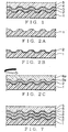
- FIG. 1 A general example of such an optical multi-layer recording medium is shown in Fig. 1, in which its cross sectional view is schematically illustrated. In this illustration, an example of a single-sided two-layer type rewritable recording medium is shown.
- a first phase change recording layer 2 is formed on one side of a substrate 1 made of material having relatively high stiffness, such as resin, for example, polycarbonate, glass and metal.
- the substrate 1 is provided with a convexo-concave portion for forming recording marks, which is formed spirally or formed in a concentric circle-shape on said one side of the substrate 1.
- the first phase change recording layer 2 located on the convexo-concave portion of the substrate 1 has a convexo-concave shape accordingly and the recording marks are formed there.
- an optically permeable intermediate layer 3 made of transparent material (normally, resin), a second phase change recording layer 4, and a cover layer 5 are formed in this sequence.
- the optically translucent intermediate layer 3 is provided with a convexo-concave portion (guide groove) for forming recording marks, which is formed spirally or formed in a concentric circle-shape on the layer 4-side of the layer 3.
- the second phase change recording layer 4 located on the convexo-concave portion of the substrate 1 has a convexo-concave shape accordingly and the recording marks are formed there.
- the second phase change recording layer 4 is protected by the cover layer 5 made of transparent material (normally, resin).
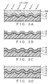
- the optical multi-layer recording medium has been produced so far as shown schematically in Figs. 2 and 3.
- the first phase change recording layer 2 is formed on the substrate 1 (see Fig. 2A) having a convex portion for forming the recording marks, which is formed by resin molding or etching, then non-cured photo-curing resin 3a is applied thereon by spin coating or the like and then, a stamper 6a is laminated thereon (see Fig. 2C) when the photo-curing resin 3a remains in its non-cured state.
- the stamper 6a is made of glass or highly transparent resin such as polycarbonate and transmits light.
- the first phase change recording layer 2 does not transmit or hardly transmit light since it has a metal reflecting layer.
- the stamper 6a is provided with a convexo-concave portion on its substrate 1-side so that a guide groove for recording is formed on the layer 4-side surface when the non-cured photo-curing resin 3a is cured and becomes the optically permeable intermediate layer 3.
- the photo-curing resin 3a is irradiated with light having a wavelength suitable to the curing through the stamper 6a, thereby curing the photo-curing resin 3a to become the optically permeable intermediate layer 3.
- the stamper 6a is taken off, then the second phase change recording layer 4 and the cover layer 5 are formed in this sequence on the optically permeable intermediate layer 3.
- the stamper 6a can not be easily separated (released) from the optically permeable intermediate layer 3, which is formed when the photo-curing resin 3a is cured.
- the stamper made of polycarbonate is employed, the stamper is hardly separated from the optically permeable intermediate layer.
- the stamper made of glass when employed, it can be easily separated from the optically permeable intermediate layer.
- This problem may be avoided by using the stamper made of glass repeatedly, however, the stamper made of glass is hard for a worker to handle and is easily broken.
- the stamper made of polycarbonate is coated with a release agent, however, this measure has drawbacks such as increase in the number of manufacturing steps including the coating step described above and a possible problem that a desired formation of the concave portion can not be carried out when dust or the like is brought in the coating step.
- the present invention is to provide a transparent stamper for molding an optical multi-layer recording medium, characterized in that the transparent stamper is made of amorphous polyolefin resin.
- the transparent stamper as described above consists of thermoplastic amorphous polyolefin resin, which can be easily formed (molded). With the construction described above, a master stamper can be used, the productivity of the stamper itself improves, the cost of the stamper can be reduced, obtaining a good separation (release) from the layer of the photo-curing resin.
- the present invention is also to provide a process for producing an optical multi-layer recording medium comprising the steps of: laminating a layer of non-cured photo-curing resin and a transparent stamper made of amorphous polyolefin resin in this sequence on a substrate; curing the non-cured photo-curing resin with light permeated through the transparent stamper; and removing the transparent stamper.
- the optical multi-layer recording medium can be produced with a good productivity and low cost.
- the resin for constituting the transparent stamper must be an amorphous polyolefin resin.
- an amorphous polyolefin resin is preferably an amorphous polyolefin resin which is capable of being accurately molded by using a master stamper made of metal or the like, for example, an amorphous polyolefin resin having glass transition point equal to or lower than 200 °C and high flowability upon molding. Since the photo-curing resin must be cured with the light permeated through the stamper, the stamper must have high permeability for the light having a wavelength region, which is necessary for the photo-curing resin to be cured.
- the stamper in order to facilitate the separation (release) of the stamper from the photo-curing resin, the stamper must have a good resistance against acid, alkali and polar organic solvent. Further, when a normal crystalline polyolefin resin is employed as the stamper material, residual stress upon molding causes stress relaxation for crystallization, rendering the stamper to be curved, thereby the stamper becomes not suitable for its transparency and flatness. Accordingly, the polyolefin resin for the material of the stamper must be amorphous.
- the amorphous polyolefin resin as described above is, for example, ZEONOR (manufactured by ZEON Corporation), ZEONEX (manufactured by ZEON Corporation), APL (manufactured by Mitsui Chemicals Co., Ltd.), APO (manufactured by Mitsui Chemicals Co., Ltd.), and ARTON (manufactured by JSR Corporation).
- a transparent stamper is molded by using a master stamper made of metal or glass, to which a necessary shape is given by means of etching or the like.
- the molding process is carried out with setting a mold temperature to be low, thereby improving the accuracy of the molding (i.e., accuracy of fine hollow portions).
- the thickness of the stamper is not basically limited to any specific value, preferably, it may be from 0.6 mm to 1.5 mm, since the photo-curing resin must be cured with the light permeated through the stamper and the stamper must have certain mechanical strength which is needed as a stamper. More preferably, it may be about 1.1 mm, thereby enabling the usage of a mold same as that used upon molding of the substrate.
- the stamper is usually reused after once being used. Although it preferably used only once, it can be used twice or more by selecting the starting resin material, by optimizing the photo-curing resin for forming the optically permeable intermediate layer and its curing condition, or by inspecting it before reuse.
- the photo-curing resin in the present invention is a resin composition, in which initiator for photo-polymerization having sensitivity to light such as visible or ultraviolet light is compounded.
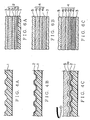
- a first phase change recording layer 2 which is a non-optically permeable layer, is formed on a substrate 1 shown in Fig. 4A, and thereafter, non-cured photo-curing resin 3a having viscosity of 50 - 800 mPs is dropped on the first phase change recording layer 2.
- a stamper 6 made of an amorphous polyolefin resin described above is put thereon as shown in Fig. 4C.
- the photo-curing resin 3a naturally spreads over.
- the photo-curing resin 3a spreads over to a specific area with a specific thickness, which can normally be set 20 - 30 ⁇ m.
- the thickness of the layer of the photo-curing resin 3a can be controlled by selecting the viscosity of the photo-curing resin besides by selecting the rotation speed and a period of time for the rotation.
- the non-cured photo-curing resin 3a and the stamper 6 made of the amorphous polyolefin resin are laminated in this sequence on the substrate having the non-optically permeable layer (i.e., first phase change recording layer 2) thereon, and thereafter, the non-cured photo-curing resin is cured with the light permeated through the stamper.
- the non-optically permeable layer i.e., first phase change recording layer 2
- the light having a wavelength, which is suitable for curing the photo-curing resin, such as a ultraviolet light is irradiated through the stamper 6 as shown in Fig. 5A, thereby curing the photo-curing resin so as to form the optically permeable intermediate layer 3.
- the stamper 6 is removed.
- the stamper 6 according to the present invention can be easily separated from the optically permeable intermediate layer 3. Even a part of the stamper 6 never remains on the optically permeable intermediate layer 3, thereby a high quality and highly reliable optical multi-layer recording medium can be produced.
- a second phase change recording layer 4 and a cover layer 5 are formed in this sequence on the optically permeable intermediate layer 3, thereby the optical multi-layer recording medium is produced.
- a partially expanded schematic illustration of the first phase change recording layer 2 as shown in Fig. 1 is shown in Fig. 6A.
- the first phase change recording layer 2 includes: a metal reflector film 2a, which is made of aluminum or silver alloy having no or almost no optical permeability and formed by a method of forming a metal film such as evaporation, chemical vapor deposition (CVD) and sputtering methods; a first dielectric film 2b; a phase change recording film 2c; and a second dielectric film 2d, which are formed on the substrate 1 in this sequence, wherein an optical characteristic of the phase change recording film 2c is changed, thereby enabling recording and erasing of information.
- a metal reflector film 2a which is made of aluminum or silver alloy having no or almost no optical permeability and formed by a method of forming a metal film such as evaporation, chemical vapor deposition (CVD) and sputtering methods
- a first dielectric film 2b a phase change recording film 2c
- a second dielectric film 2d which are formed on the substrate 1 in this sequence, wherein an optical characteristic of the phase change recording film 2
- the second phase change recording layer 4 there are two types.
- the first and second types are schematically shown in Figs. 6B and 6C, respectively.
- the second phase change recording layer 4 includes: a first dielectric film 4a; a phase change recording film 4b; and a second dielectric film 4c, which are formed on the optically permeable intermediate layer 3 in this sequence, while as for the second type, the second phase change recording layer 4 includes: a dielectric film 4d; a translucent metal film 4e; a first dielectric film 4a; a phase change recording film 4b; and a second dielectric film 4c, which are formed on the optically permeable intermediate layer 3 in this sequence.
- one or more recording layers besides the first and second phase change recording layers may be a recording layer, in which a reflector layer or translucent reflector layer consisting of metal or dielectric and a dye layer are combined, or may be a recording layer for exclusive regenerative use, in which a reflector layer or translucent reflector layer consisting of metal or dielectric and a ROM mark layer are combined.
- the stamper according to the present invention can be used to form the optically permeable intermediate layer.
- the stamper according to the present invention can also be used to form the cover layer 5 shown in Fig. 1, showing that such a use is included in a scope of a process for producing an optical multi-layer recording medium according to the present invention.
- the photo-curing resin 5a is dropped on an intermediate product of the optical multi-layer recording medium, and thereafter the stamper 7 made of amorphous polyolefin resin is put thereon with the intermediate product being rotated as shown in Fig. 8A.
- the thickness of the resin layer to be formed can be controlled by selecting the viscosity of the resin, the rotation speed and a period of time for the rotation.
- the thickness of the cover layer is 60 - 110 ⁇ m, which is larger than the thickness of the optically permeable intermediate layer 3. Therefore, preferably, a photo-curing resin having viscosity higher than that of the photo-curing resin, which is used for forming the optically permeable intermediate layer 3, is used for forming the cover layer.
- the light having a wavelength, which is suitable for curing the photo-curing resin, such as a ultraviolet light is irradiated through the stamper 7 as shown in Fig. 8B, thereby curing the photo-curing resin 5a so as to form the cover layer 5.
- a transparent stamper made of amorphous polyolefin resin according the present invention was prepared with a master stamper.
- the thickness of the transparent stamper was 1.1 mm.
- One side of the stamper was provided with convex and concave portions (maximum height: 20 nm) for forming guide grooves for the second phase change recording layer, which were arranged concentrically.
- a photo (ultraviolet light)-curing resin was dropped on a first phase change recording layer (see Fig. 4B), which was already formed on a polycarbonate substrate (thickness: 1.1 mm). Thereafter, the stamper made of amorphous polyolefin resin as prepared above was put thereon, thereafter the substrate was rotated so as to remove the excess photo (ultraviolet light)-curing resin.
- the optically permeable intermediate layer thus formed was evaluated.
- FIGS 9A and 9B reveal that the guide groove of the optically permeable intermediate layer formed by using the stamper according to the present invention accurately reproduced the guide groove of the master stamper similarly to the substrate for molding.
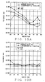
- a photo (ultraviolet light)-curing resin (MP121 manufactured by Mitsubishi Rayon Co., Ltd.) was dropped on a polycarbonate substrate (thickness: 1.1 mm), on which a first phase change recording layer was not formed. Thereafter, a stamper (thickness: 0.3 mm) made of nickel was put thereon, thereafter the substrate was rotated so as to remove the excess photo (ultraviolet light)-curing resin.
- Figure 10A shows a change in the thickness of the optically permeable intermediate layer for the radial direction of the intermediate layer, which was measured from the center of the test sample obtained by using the stamper made of nickel
- Figure 10B shows a change in the thickness of the optically permeable intermediate layer for the radial direction of the intermediate layer, which was measured from the center of the test sample obtained by using the stamper made of amorphous polyolefin resin according to the present invention.
- Figs. 10A and 10B reveal that when the stamper according to the present invention was used, the variation in the thickness of the optically permeable intermediate layer for its radial direction could significantly be reduced and also the variation in the thickness (that is, a difference between the maximum thickness and the minimum thickness for each value of the radius that is a distance from the rotation center) of the optically permeable intermediate layer for its circumferential direction, which causes an error in recording and reading in an optical recording medium, could be reduced in comparison with the case when the stamper made of nickel was used.
- the stamper according to the present invention is rotated when it is put on the non-cured photo-curing resin layer. At this time, the substrate is slightly deformed due to the rotation.
- the stamper according to the present invention is used, the stamper is considered to be deformed as the substrate is deformed because the stamper is made of amorphous polyolefin resin, which is comparatively soft material.
- the optically permeable intermediate layer having small variation in the thickness for its radial and circumferential directions is considered to be formed.
- the stamper made of a material having high stiffness such as nickel is used, the optically permeable intermediate layer having large variation in its thickness seems to be formed since the deformation as described above does not take place.
Landscapes
- Engineering & Computer Science (AREA)
- Manufacturing & Machinery (AREA)
- Mechanical Engineering (AREA)
- Manufacturing Optical Record Carriers (AREA)
- Optical Record Carriers And Manufacture Thereof (AREA)
- Casting Or Compression Moulding Of Plastics Or The Like (AREA)
Applications Claiming Priority (2)
| Application Number | Priority Date | Filing Date | Title |
|---|---|---|---|
| JP2002196096A JP2004039136A (ja) | 2002-07-04 | 2002-07-04 | 光学多層記録媒体成形用透明スタンパおよび光学多層記録媒体の製造方法 |
| JP2002196096 | 2002-07-04 |
Publications (2)
| Publication Number | Publication Date |
|---|---|
| EP1378898A1 EP1378898A1 (en) | 2004-01-07 |
| EP1378898B1 true EP1378898B1 (en) | 2006-11-22 |
Family
ID=29720299
Family Applications (1)
| Application Number | Title | Priority Date | Filing Date |
|---|---|---|---|
| EP03013748A Revoked EP1378898B1 (en) | 2002-07-04 | 2003-06-17 | Transparent stamper for molding optical multi-layer recording medium and process for producing optical multi-layer recording medium |
Country Status (5)
| Country | Link |
|---|---|
| US (1) | US20040004300A1 (enExample) |
| EP (1) | EP1378898B1 (enExample) |
| JP (1) | JP2004039136A (enExample) |
| CN (1) | CN1469364A (enExample) |
| DE (1) | DE60309782T2 (enExample) |
Families Citing this family (23)
| Publication number | Priority date | Publication date | Assignee | Title |
|---|---|---|---|---|
| CN100421163C (zh) * | 2003-11-12 | 2008-09-24 | 三菱化学媒体股份有限公司 | 制备光学记录介质的方法和透光性压模 |
| DE102004025314A1 (de) * | 2004-05-19 | 2005-12-29 | Fraunhofer-Gesellschaft zur Förderung der angewandten Forschung e.V. | Verfahren zur Herstellung eines optischen Speichermediums und optisches Speichermedium |
| WO2006009161A1 (ja) * | 2004-07-21 | 2006-01-26 | Matsushita Electric Industrial Co., Ltd. | 多層情報記録媒体及びその製造方法 |
| CN101128300B (zh) * | 2005-02-28 | 2010-09-29 | 日本瑞翁株式会社 | 固化性树脂成型体的制造方法以及固化树脂成型体 |
| JP2006313077A (ja) * | 2005-05-06 | 2006-11-16 | Ricoh Co Ltd | 光学積層体検査方法,光学積層体製造方法および光学積層体検査装置ならびに光学積層体製造装置 |
| DE602005010839D1 (de) * | 2005-06-10 | 2008-12-18 | Obducat Ab | Verfahren zum Kopieren eines Modells |
| JP4827848B2 (ja) * | 2005-08-30 | 2011-11-30 | パナソニック株式会社 | 多層情報記録媒体の製造方法、並びに多層情報記録媒体の製造装置とこの製造装置を構成する多層情報記録媒体製造用スクリーン |
| JP2007133970A (ja) * | 2005-11-10 | 2007-05-31 | Canon Inc | 光記録媒体およびその製造方法 |
| CN101300632B (zh) * | 2005-11-18 | 2011-05-18 | 三菱化学媒体股份有限公司 | 光记录介质的制造方法和制造装置 |
| JP4529895B2 (ja) * | 2005-12-22 | 2010-08-25 | ソニー株式会社 | 光ディスクの製造方法 |
| WO2008041526A1 (en) | 2006-09-26 | 2008-04-10 | Mitsubishi Kagaku Media Co., Ltd. | Method and apparatus for manufacturing optical recording medium |
| DE102007007323A1 (de) * | 2007-02-14 | 2008-08-21 | Singulus Technologies Ag | Verfahren zur Herstellung optischer Datenträger mit mehreren Informationsschichten |
| JP2008269720A (ja) * | 2007-04-23 | 2008-11-06 | Canon Inc | 透光性スタンパ、透光性スタンパの製造方法及び多層光記録媒体の製造方法 |
| JPWO2009101883A1 (ja) * | 2008-02-13 | 2011-06-09 | コニカミノルタオプト株式会社 | ハイブリッド光学素子集合体の製造方法 |
| CN101256354B (zh) * | 2008-04-14 | 2012-05-23 | 友达光电股份有限公司 | 压模及其制造方法 |
| NL2005254A (en) | 2009-09-22 | 2011-03-23 | Asml Netherlands Bv | Imprint lithography method and apparatus. |
| JP4829360B2 (ja) * | 2010-04-27 | 2011-12-07 | 株式会社東芝 | スタンパーの製造方法 |
| JPWO2016051928A1 (ja) * | 2014-10-04 | 2017-09-28 | 富山県 | インプリント用テンプレート及びその製造方法 |
| US10034519B2 (en) | 2016-06-16 | 2018-07-31 | Adidas Ag | UV curable lattice microstructure for footwear |
| US11122847B2 (en) | 2017-04-24 | 2021-09-21 | Nike, Inc. | Article with UV radiation curable material adhered to textile and method of making the same |
| EP3576919B1 (en) | 2017-04-24 | 2020-06-17 | NIKE Innovate C.V. | Transparent tooling mold and process for uv radiation curable rubber |
| US11136475B2 (en) | 2017-04-24 | 2021-10-05 | Nike, Inc. | Articles and components with UV radiation curable elastomeric materials and methods of making the same |
| CN110582396A (zh) | 2017-04-24 | 2019-12-17 | 耐克创新有限合伙公司 | 具有uv辐射可固化材料的服装和运动装备及其制造方法 |
Family Cites Families (2)
| Publication number | Priority date | Publication date | Assignee | Title |
|---|---|---|---|---|
| JPH0823941B2 (ja) * | 1988-11-08 | 1996-03-06 | パイオニア株式会社 | 光学式情報記録担体及びその製造方法 |
| US5175030A (en) * | 1989-02-10 | 1992-12-29 | Minnesota Mining And Manufacturing Company | Microstructure-bearing composite plastic articles and method of making |
-
2002
- 2002-07-04 JP JP2002196096A patent/JP2004039136A/ja active Pending
-
2003
- 2003-05-29 US US10/446,930 patent/US20040004300A1/en not_active Abandoned
- 2003-06-17 DE DE60309782T patent/DE60309782T2/de not_active Revoked
- 2003-06-17 EP EP03013748A patent/EP1378898B1/en not_active Revoked
- 2003-06-27 CN CNA031485057A patent/CN1469364A/zh active Pending
Also Published As
| Publication number | Publication date |
|---|---|
| US20040004300A1 (en) | 2004-01-08 |
| EP1378898A1 (en) | 2004-01-07 |
| DE60309782D1 (de) | 2007-01-04 |
| JP2004039136A (ja) | 2004-02-05 |
| CN1469364A (zh) | 2004-01-21 |
| DE60309782T2 (de) | 2007-03-01 |
Similar Documents
| Publication | Publication Date | Title |
|---|---|---|
| EP1378898B1 (en) | Transparent stamper for molding optical multi-layer recording medium and process for producing optical multi-layer recording medium | |
| US5509991A (en) | Method of producing an optical disk having an integrated label layer | |
| US5669995A (en) | Method for writing and reading data on a multi-layer recordable interferometric optical disc and method for fabricating such | |
| JP3338660B2 (ja) | 光ディスク | |
| JPH0991765A (ja) | 両面多層光ディスク及びその製造方法 | |
| US20030179693A1 (en) | Single-sided double layer optical disc, and method and apparatus for manufacturing the same | |
| KR20010053544A (ko) | 디스크형 다층 정보 기록 매체 및 그 제조 방법 | |
| US6440516B1 (en) | Optical disc | |
| US6800224B2 (en) | Production process of optical disc and optical disc produced thereby | |
| JP2008269720A (ja) | 透光性スタンパ、透光性スタンパの製造方法及び多層光記録媒体の製造方法 | |
| US20080241525A1 (en) | Stamper for optical information recording medium, master for magnetic transfer, and manufacturing methods thereof | |
| JP4088884B2 (ja) | 光ディスクの製造方法 | |
| WO2006003666A2 (en) | Multilayer optical disc and method and apparatus for making same | |
| JP2000036135A (ja) | 多層情報記録媒体の製造方法 | |
| JP4360269B2 (ja) | 多層光ディスクの製造方法 | |
| WO2003056553A1 (en) | Multi-layered optical recording medium and multi-layered optical recording medium manufacturing method | |
| JP2009277266A (ja) | 光ディスク記録媒体の製造方法 | |
| KR100962743B1 (ko) | 광학 기록 매체 및 그 제조 방법 | |
| US20040247817A1 (en) | Optical disk and method for manufacturing the same | |
| CN101374650A (zh) | 制备多层光记录介质的方法和压模以及制造该压模的方法 | |
| JP2007234092A (ja) | 光ディスク及び光ディスクの製造方法 | |
| US5406544A (en) | Low cost substrate for bump-forming recording media | |
| US20060134369A1 (en) | Optical disc and method of producing the same | |
| US20050271853A1 (en) | Optical recording medium and method of manufacturing the same | |
| KR20100112796A (ko) | 멀티 레이어 디스크, 그 제조방법과 제조장치 |
Legal Events
| Date | Code | Title | Description |
|---|---|---|---|
| PUAI | Public reference made under article 153(3) epc to a published international application that has entered the european phase |
Free format text: ORIGINAL CODE: 0009012 |
|
| AK | Designated contracting states |
Kind code of ref document: A1 Designated state(s): AT BE BG CH CY CZ DE DK EE ES FI FR GB GR HU IE IT LI LU MC NL PT RO SE SI SK TR |
|
| AX | Request for extension of the european patent |
Extension state: AL LT LV MK |
|
| 17P | Request for examination filed |
Effective date: 20031215 |
|
| 17Q | First examination report despatched |
Effective date: 20040316 |
|
| AKX | Designation fees paid |
Designated state(s): DE FR GB |
|
| GRAP | Despatch of communication of intention to grant a patent |
Free format text: ORIGINAL CODE: EPIDOSNIGR1 |
|
| RIN1 | Information on inventor provided before grant (corrected) |
Inventor name: HANZAWA, SHINICHI Inventor name: TAKISHITA, TOSHIHIKO Inventor name: YAMAGUCHI, MASATAKA |
|
| GRAS | Grant fee paid |
Free format text: ORIGINAL CODE: EPIDOSNIGR3 |
|
| GRAA | (expected) grant |
Free format text: ORIGINAL CODE: 0009210 |
|
| AK | Designated contracting states |
Kind code of ref document: B1 Designated state(s): DE FR GB |
|
| REG | Reference to a national code |
Ref country code: GB Ref legal event code: FG4D |
|
| REF | Corresponds to: |
Ref document number: 60309782 Country of ref document: DE Date of ref document: 20070104 Kind code of ref document: P |
|
| EN | Fr: translation not filed | ||
| PGFP | Annual fee paid to national office [announced via postgrant information from national office to epo] |
Ref country code: DE Payment date: 20070730 Year of fee payment: 5 |
|
| PLBI | Opposition filed |
Free format text: ORIGINAL CODE: 0009260 |
|
| 26 | Opposition filed |
Opponent name: VOSSIUS & PARTNER Effective date: 20070817 |
|
| PLAX | Notice of opposition and request to file observation + time limit sent |
Free format text: ORIGINAL CODE: EPIDOSNOBS2 |
|
| GBPC | Gb: european patent ceased through non-payment of renewal fee |
Effective date: 20070617 |
|
| PG25 | Lapsed in a contracting state [announced via postgrant information from national office to epo] |
Ref country code: FR Free format text: LAPSE BECAUSE OF FAILURE TO SUBMIT A TRANSLATION OF THE DESCRIPTION OR TO PAY THE FEE WITHIN THE PRESCRIBED TIME-LIMIT Effective date: 20070713 |
|
| PG25 | Lapsed in a contracting state [announced via postgrant information from national office to epo] |
Ref country code: GB Free format text: LAPSE BECAUSE OF NON-PAYMENT OF DUE FEES Effective date: 20070617 |
|
| RDAF | Communication despatched that patent is revoked |
Free format text: ORIGINAL CODE: EPIDOSNREV1 |
|
| RDAG | Patent revoked |
Free format text: ORIGINAL CODE: 0009271 |
|
| STAA | Information on the status of an ep patent application or granted ep patent |
Free format text: STATUS: PATENT REVOKED |
|
| 27W | Patent revoked |
Effective date: 20080605 |
|
| PG25 | Lapsed in a contracting state [announced via postgrant information from national office to epo] |
Ref country code: FR Free format text: LAPSE BECAUSE OF FAILURE TO SUBMIT A TRANSLATION OF THE DESCRIPTION OR TO PAY THE FEE WITHIN THE PRESCRIBED TIME-LIMIT Effective date: 20061122 |