EP1378772A2 - Method of manufacturing tapered optical waveguide - Google Patents
Method of manufacturing tapered optical waveguide Download PDFInfo
- Publication number
- EP1378772A2 EP1378772A2 EP03014458A EP03014458A EP1378772A2 EP 1378772 A2 EP1378772 A2 EP 1378772A2 EP 03014458 A EP03014458 A EP 03014458A EP 03014458 A EP03014458 A EP 03014458A EP 1378772 A2 EP1378772 A2 EP 1378772A2
- Authority
- EP
- European Patent Office
- Prior art keywords
- tapered
- core layer
- photo
- layer
- forming
- Prior art date
- Legal status (The legal status is an assumption and is not a legal conclusion. Google has not performed a legal analysis and makes no representation as to the accuracy of the status listed.)
- Withdrawn
Links
Images


Classifications
-
- G—PHYSICS
- G02—OPTICS
- G02B—OPTICAL ELEMENTS, SYSTEMS OR APPARATUS
- G02B6/00—Light guides; Structural details of arrangements comprising light guides and other optical elements, e.g. couplings
- G02B6/10—Light guides; Structural details of arrangements comprising light guides and other optical elements, e.g. couplings of the optical waveguide type
- G02B6/12—Light guides; Structural details of arrangements comprising light guides and other optical elements, e.g. couplings of the optical waveguide type of the integrated circuit kind
-
- G—PHYSICS
- G02—OPTICS
- G02B—OPTICAL ELEMENTS, SYSTEMS OR APPARATUS
- G02B6/00—Light guides; Structural details of arrangements comprising light guides and other optical elements, e.g. couplings
- G02B6/10—Light guides; Structural details of arrangements comprising light guides and other optical elements, e.g. couplings of the optical waveguide type
- G02B6/12—Light guides; Structural details of arrangements comprising light guides and other optical elements, e.g. couplings of the optical waveguide type of the integrated circuit kind
- G02B6/122—Basic optical elements, e.g. light-guiding paths
- G02B6/1228—Tapered waveguides, e.g. integrated spot-size transformers
-
- G—PHYSICS
- G02—OPTICS
- G02B—OPTICAL ELEMENTS, SYSTEMS OR APPARATUS
- G02B6/00—Light guides; Structural details of arrangements comprising light guides and other optical elements, e.g. couplings
- G02B6/10—Light guides; Structural details of arrangements comprising light guides and other optical elements, e.g. couplings of the optical waveguide type
- G02B6/12—Light guides; Structural details of arrangements comprising light guides and other optical elements, e.g. couplings of the optical waveguide type of the integrated circuit kind
- G02B6/13—Integrated optical circuits characterised by the manufacturing method
- G02B6/136—Integrated optical circuits characterised by the manufacturing method by etching
Definitions
- the present invention relates to a method of manufacturing an optical waveguide, and more particularly to a method of manufacturing a tapered optical waveguide, through which two optical waveguides of different sizes are connected optically.
- a waveguide is an indispensable element of an integrated optical component in a high-speed optical-communication network.
- the waveguide has wide applications used in optical-power splitters, optical couplers, optical modulators, interferometer-based switches, semiconductor lasers, and planar devices for dense wavelength-division-multiplexing communication.
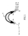
- FIG. 1 is a schematic diagram of a wavelength-division multiplexer utilizing an arrayed waveguide grating.
- the waveguide grating includes input and output waveguides 11a and 11b, two planar waveguides 13a and 13b, and an arrayed waveguide grating 15.
- optical waveguides with different constructions are connected with each other directly, the difference in the width of adjoining optical waveguides generates optical loss.
- This n abrupt change between the connecting joints causes an optical signal to be radiated instead of being propagated through the waveguides. This radiation of the optical signal generates additional loss and noise, thereby causing cross-talk between different channels.
- FIG. 2 is a schematic view of a conventional linear tapered waveguide.
- the tapered waveguide 22 has a width increasing from one end of a base waveguide 21 to the other end of a target waveguide 23.
- a lateral taper and a vertical taper should be simultaneously realized in order to lower a coupling loss caused by a mode mismatch.
- a thin film having a thickness profile is deposited and then etched by means of a shadow mask, thereby forming a tapered waveguide.
- a thin film having a uniform thickness is etched by a shadow mask, while an etched depth of the thin film is adjusted to allow the thin film to have a thickness profile, then the thin film with the thickness profile is etched again, thereby forming a tapered waveguide.
- it is difficult to control a position, inclination, shape, etc., of a tapered section and to mass-produce tapered waveguides as the shadow mask must be installed above a substrate.
- a thin film is deposited on a stepped substrate, then a flattening process is performed so as to enable the thin film to have a thickness profile. Finally, the thin film having a thickness profile is etched, thereby forming a tapered waveguide.
- a separate flattening process is necessary.
- heat is locally applied to the waveguide after a waveguide with a uniform thickness is formed, thereby enlarging a predetermined portion of the waveguide.
- a precise control is impossible in forming the waveguide.
- the present invention has been made to solve the above-mentioned problems occurring in the prior art, by providing a method of manufacturing a tapered optical waveguide, in which an optical waveguide having a construction tapered in vertical and horizontal side views can be manufactured through a simple manufacturing process.
- this invention provides a method of manufacturing a tapered optical waveguide, the method comprising the steps of: (1) forming an underclad layer and a core layer in sequence on a substrate; (2) forming a photo-resist pattern having an inclined profile on the core layer by means of a gray-scale mask; (3) etching the photo-resist pattern and the core layer to form a first tapered core layer having a side profile equal to that of the tapered optical waveguide to be manufactured; (4) forming a mask pattern on the first tapered core layer, the mask pattern having a planar profile equal to that of the tapered optical waveguide to be manufactured; (5) etching the first tapered core layer utilizing the mask pattern as an etching mask, thereby forming a second tapered core layer; and, (6) forming an overclad layer on the second tapered core layer.
- the inclined profile of the photo-resist pattern can be controlled by adjusting ultraviolet-ray transmittance of the gray-scale mask.
- an inclination of the side profile of the first tapered core layer can be controlled by adjusting an etching-selection ratio between the photo-resist and the core layer.
- Another aspect of the present invention provides a method of manufacturing a tapered optical waveguide, the method comprising the steps of: (1) forming an underclad layer on a substrate; (2) forming a photo-resist pattern having an inclined profile on the underclad layer by means of a gray-scale mask; (3) etching the photo-resist pattern and the underclad layer to form a tapered underclad layer having a side profile equal to that of the tapered optical waveguide to be manufactured; (4) depositing a core layer on the tapered underclad layer and flattening the core layer, thereby forming a first tapered core layer; (5) forming a mask pattern on the first tapered core layer, the mask pattern having a planar profile equal to that of the tapered optical waveguide to be manufactured; (6) etching the first tapered core layer utilizing the mask pattern as an etching mask, thereby forming a second tapered core layer; and, (7) forming an overclad layer on the second tapered core layer.
- FIGs. 3A to 3G are sectional views showing the process of manufacturing a tapered waveguide according to an embodiment of the present invention, in which a core layer having a profile inclined in vertical and horizontal side views is formed.
- the expression “tapered in the vertical side” means that the profile is inclined rightward or leftward from a side view
- the expression “tapered in the horizontal side” means that the profile is inclined rightward or leftward from a planar? view.
- an underclad layer 32 and a core layer 33 are deposited in sequence on a substrate 31.
- a photo-resist 34 is applied on the core layer 33 and then exposed to light through a gray-scale mask 100.
- a photo-resist profile having a desired shape can be obtained.
- FIG. 3C shows a state in which a photo-resist pattern 34' has been formed as described above.
- a core layer 33' having an inclined profile is formed by dry etching the photo-resist pattern 34' and the core layer 33.
- the shape of the photo-resist pattern 34' is transcribed to the core layer.
- the degree of transcription changes according to the etching-selection ratio between the photo-resist and the core layer. For example, when the etching-selection ratio between the photo-resist and the core layer is 1:1, the profile of the photo-resist pattern 34' is transcribed intact to the core layer 33. Therefore, in order to obtain a core layer having a desired profile, both the profile of the photo-resist pattern 34' and the etching-selection ratio must be considered simultaneously.
- a photo-resist is applied to the core layer 33' that is tapered when viewed from the vertical side, then a general photolithography is performed, thereby forming a photo-resist mask pattern 35 for forming an optical waveguide tapered from the horizontal side view.
- FIG. 3F is a planar view of the lamination shown in FIG. 3E, in which the shape of the photo-resist mask pattern 35 for forming the optical waveguide tapered when viewed from the horizontal side.
- a waveguide 33" is formed by etching the core layer 33' under the photo-resist mask pattern 35 utilizing the photo-resist mask pattern 35 as a mask, then an overclad layer 36 is deposited on the waveguide 33".
- the photo-resist mask pattern 35 functions as an etching mask.
- a hard-etching mask may be utilized. That is, a metal or inorganic material, capable of functioning as a hard mask, is deposited on the core layer before applying photo-resist for forming a mask pattern, and a photo-resist mask pattern is formed on the deposited metal or inorganic material through a photolithography.
- the deposited metal or inorganic material is etched utilizing the photo-resist mask pattern formed in the way described above, thereby forming a hard-mask pattern.
- the hard-mask pattern may be utilized as an etching mask in etching the core layer.
- FIG. 4 is a perspective view of a core layer on an underclad layer formed through the process shown in FIGs. 3A to 3G which is tapered in the vertical side view (in a side-sectional view) and horizontal side view (in a planar view).
- FIGs. 5A to 5F are sectional views showing the process of manufacturing a tapered waveguide according to another embodiment of the present invention, in which the tapered waveguide is manufactured by forming an inclined profile on an underclad layer.
- an underclad layer 52 is deposited on a substrate 51, as shown in FIG. SA.
- a photo-resist 54 is applied on the underclad layer 52 and then exposed to light through a gray-scale mask 100.
- a photo-resist profile having a desired shape can be obtained.
- FIG. 5C shows a state in which a photo-resist pattern 54' has been formed by exposing and developing the photo-resist 54 utilizing the gray-scale mask 100.
- an underclad layer 52' having an inclined profile is formed by dry etching the underclad layer 52 utilizing the photo-resist pattern 54' as an etching mask.
- the shape of the photo-resist pattern 54' is transcribed to the underclad layer.
- the degree of transcription changes according to an etching-selection ratio between the photo-resist and the underclad layer.
- the profile of the photo-resist pattern 54' is transcribed intact to the underclad layer. Therefore, in order to obtain an underclad layer having a desired profile, both the profile of the photo-resist pattern 54' and the etching-selection ratio must be considered simultaneously.
- a core layer 53 is deposited on the underclad layer 52' having an inclined profile, then the deposited core layer 53 is flattened through a flattening step.
- a waveguide 53" is formed by etching the core layer, then an overclad layer 56 is deposited on the waveguide 53".
- the core layer may be etched utilizing a photo-resist mask pattern having a profile inclined from the horizontal side or a hard-etching mask in a similar matter (or manner?) as the previous embodiment.
- the manufacturing process is relatively simple and the shape of the waveguide can be controlled precisely. Therefore, the method according to the present invention remarkably can reduce a coupling loss due to spot-size mismatch between optical fibers, composite optical-semiconductor devices, and quartz-based optical-integrated circuits.
Landscapes
- Physics & Mathematics (AREA)
- Engineering & Computer Science (AREA)
- Microelectronics & Electronic Packaging (AREA)
- General Physics & Mathematics (AREA)
- Optics & Photonics (AREA)
- Power Engineering (AREA)
- Optical Integrated Circuits (AREA)
Abstract
Description
- FIG. 1
- is a schematic view of a wavelength-division multiplexer according to a prior art;
- FIG. 2
- is a schematic view of the prior-art tapered waveguide;
- FIGs. 3A to 3G
- are sectional views showing a process of manufacturing a tapered waveguide according to an embodiment of the present invention;
- FIG. 4
- is a perspective view of a tapered optical waveguide manufactured through the process shown in FIGs. 3A to 3G; and,
- FIGs. 5A to 5F
- are sectional views showing a method of manufacturing a tapered waveguide according to another embodiment of the present invention.
Claims (6)
- A method of manufacturing a tapered optical waveguide, the method comprising the steps of:(1) forming an underclad layer and a core layer on a substrate;(2) forming a photo-resist pattern having an inclined profile on the core layer by exposing a light on the core layer via a gray-scale mask;(3) etching the photo-resist pattern and the core layer to form a first tapered core layer;(4) forming a mask pattern on the first tapered core layer;(5) etching the first tapered core layer utilizing the mask pattern as an etching mask, thereby forming a second tapered core layer; and,(6) forming an overclad layer on the second tapered core layer.
- The method of claim 1, wherein the inclined profile of the photo-resist pattern can be controlled by adjusting ultraviolet-ray transmittance through the gray-scale mask.
- The method of claim 1, wherein an inclination of the side profile of the first tapered core layer can be controlled by adjusting an etching-selection ratio between the photo-resist and the core layer.
- A method of manufacturing a tapered optical waveguide, the method comprising the steps of:(1) forming an underclad layer on a substrate;(2) forming a photo-resist pattern having an inclined profile on the underclad layer by exposing a light via a gray-scale mask;(3) etching the photo-resist pattern and the underclad layer to form a tapered underclad layer;(4) depositing a core layer on the tapered underclad layer and flattening the core layer, thereby forming a first tapered core layer;(5) forming a mask pattern on the first tapered core layer;(6) etching the first tapered core layer utilizing the mask pattern as an etching mask, thereby forming a second tapered core layer; and,(7) forming an overclad layer on the second tapered core layer.
- The method of claim 4, wherein the inclined profile of the photo-resist pattern can be controlled by adjusting ultraviolet-ray transmittance through the gray-scale mask.
- The method of claim 4, wherein an inclination of the side profile of the tapered underclad layer can be controlled by adjusting an etching-selection ratio between the photo-resist and the underclad layer.
Applications Claiming Priority (2)
| Application Number | Priority Date | Filing Date | Title |
|---|---|---|---|
| KR10-2002-0038169A KR100450935B1 (en) | 2002-07-03 | 2002-07-03 | Method for fabricating tapered waveguide |
| KR2002038169 | 2002-07-03 |
Publications (2)
| Publication Number | Publication Date |
|---|---|
| EP1378772A2 true EP1378772A2 (en) | 2004-01-07 |
| EP1378772A3 EP1378772A3 (en) | 2004-12-22 |
Family
ID=29720336
Family Applications (1)
| Application Number | Title | Priority Date | Filing Date |
|---|---|---|---|
| EP03014458A Withdrawn EP1378772A3 (en) | 2002-07-03 | 2003-07-01 | Method of manufacturing tapered optical waveguide |
Country Status (5)
| Country | Link |
|---|---|
| US (1) | US6767756B2 (en) |
| EP (1) | EP1378772A3 (en) |
| JP (1) | JP2004038162A (en) |
| KR (1) | KR100450935B1 (en) |
| CN (1) | CN1208637C (en) |
Cited By (4)
| Publication number | Priority date | Publication date | Assignee | Title |
|---|---|---|---|---|
| AT502050B1 (en) * | 2006-02-10 | 2007-01-15 | Photeon Technologies Gmbh | Manufacturing method for light coupling device, involves placing waveguide layer on substrate so that orientation of main etching rate of inclination of wedge angle relates perpendicular to substrate surface |
| WO2008140628A1 (en) * | 2007-05-09 | 2008-11-20 | Lucent Technologies Inc. | Optical coupling structure |
| CN104793288A (en) * | 2015-04-30 | 2015-07-22 | 上海美维科技有限公司 | Manufacturing method of printed circuit boards with optical waveguide couplers |
| WO2015176024A1 (en) * | 2014-05-16 | 2015-11-19 | Tyco Electronics Corporation | Mode size converters and methods of fabricating the same |
Families Citing this family (27)
| Publication number | Priority date | Publication date | Assignee | Title |
|---|---|---|---|---|
| US7046879B2 (en) * | 2002-11-27 | 2006-05-16 | General Electric Company | Optical via for three dimensional interconnection |
| GB2402494A (en) * | 2003-06-05 | 2004-12-08 | Alcatel Optronics Uk Ltd | Integrated optic device with cladding having mesa formations |
| KR100664307B1 (en) * | 2004-08-13 | 2007-01-04 | 삼성전자주식회사 | Shadow mask and manufacturing method of vertical tapering structure using same |
| JP4639810B2 (en) * | 2005-01-17 | 2011-02-23 | ソニー株式会社 | Semiconductor device, substrate manufacturing method, and electronic apparatus |
| JP4847176B2 (en) * | 2006-03-29 | 2011-12-28 | 住友大阪セメント株式会社 | Light control element and manufacturing method thereof |
| US7343054B1 (en) * | 2007-01-04 | 2008-03-11 | Fujitsu Limited | Integrated electro-optic module for high speed data transmission |
| KR100873275B1 (en) * | 2007-03-19 | 2008-12-11 | 매그나칩 반도체 유한회사 | Manufacturing Method of Image Sensor |
| JP2010128109A (en) * | 2008-11-26 | 2010-06-10 | Furukawa Electric Co Ltd:The | Ssc chip, fiber array with ssc, plc module with ssc, and method for manufacturing ssc chip |
| DE112008004257T5 (en) * | 2008-12-29 | 2013-05-29 | Hewlett-Packard Development Company, L.P. | SYSTEMS AND METHOD OF CARRIER DEVICE FOR PLACING THERMAL INTERFACE MATERIALS |
| JP5573626B2 (en) * | 2010-11-22 | 2014-08-20 | 日立化成株式会社 | Manufacturing method of optical waveguide |
| KR20120067627A (en) * | 2010-12-16 | 2012-06-26 | 한국전자통신연구원 | Method of forming optical coupler |
| US9268089B2 (en) * | 2011-04-21 | 2016-02-23 | Octrolix Bv | Layer having a non-linear taper and method of fabrication |
| EP2581772A1 (en) * | 2011-10-14 | 2013-04-17 | Astrium Limited | A spectrometer |
| JP5145469B2 (en) * | 2012-02-24 | 2013-02-20 | 日本航空電子工業株式会社 | Optical waveguide device and manufacturing method thereof |
| JP6044174B2 (en) * | 2012-08-10 | 2016-12-14 | 日立化成株式会社 | Optical waveguide manufacturing method and optical waveguide |
| JP6044175B2 (en) * | 2012-08-10 | 2016-12-14 | 日立化成株式会社 | Optical waveguide manufacturing method and optical waveguide |
| TWI584008B (en) * | 2015-07-23 | 2017-05-21 | 國立中山大學 | Optical waveguide structure and manufacturing method thereof |
| US20170097470A1 (en) * | 2015-10-02 | 2017-04-06 | Jia Jiang | Optical Coupling Adaptor for Optical Signal Coupling Between Photonic Integrated Circuit and Optical Fiber |
| CN107688211B (en) * | 2016-08-04 | 2020-09-25 | 苏州旭创科技有限公司 | Optical waveguide device and manufacturing method thereof |
| CN106371170A (en) * | 2016-10-26 | 2017-02-01 | 中国科学院半导体研究所 | Array waveguide type light path conversion interconnection chip |
| CN106680935B (en) * | 2016-11-24 | 2019-03-05 | 中国电子科技集团公司第五十五研究所 | Efficient coupling structure and production method between a kind of silicon substrate optical waveguide |
| US10809456B2 (en) | 2018-04-04 | 2020-10-20 | Ii-Vi Delaware Inc. | Adiabatically coupled photonic systems with fan-out interposer |
| JP2021148852A (en) * | 2020-03-17 | 2021-09-27 | 沖電気工業株式会社 | Photoelectric fusion module and manufacturing method therefor |
| CN114815061B (en) * | 2022-06-01 | 2022-12-30 | 中国科学技术大学 | Preparation method of indium phosphide vertical wedge-shaped structure in spot-size converter |
| US12596229B2 (en) * | 2022-08-12 | 2026-04-07 | Purdue Research Foundation | 3D tapered nanophotonic waveguide to fiber edge coupler |
| CN115863164B (en) * | 2023-03-02 | 2023-08-04 | 浙江大学杭州国际科创中心 | Etching processing method and device and semiconductor device |
| CN116609881A (en) * | 2023-04-13 | 2023-08-18 | 上海大学 | Optical waveguide preparation method with conical XY directions |
Family Cites Families (18)
| Publication number | Priority date | Publication date | Assignee | Title |
|---|---|---|---|---|
| US3779628A (en) * | 1972-03-30 | 1973-12-18 | Corning Glass Works | Optical waveguide light source coupler |
| US4855255A (en) * | 1988-03-23 | 1989-08-08 | Massachusetts Institute Of Technology | Tapered laser or waveguide optoelectronic method |
| US4944838A (en) * | 1989-08-03 | 1990-07-31 | At&T Bell Laboratories | Method of making tapered semiconductor waveguides |
| US4938841A (en) * | 1989-10-31 | 1990-07-03 | Bell Communications Research, Inc. | Two-level lithographic mask for producing tapered depth |
| JP3019271B2 (en) * | 1991-04-05 | 2000-03-13 | 日本電信電話株式会社 | Optical waveguide formation method |
| JPH05182948A (en) * | 1992-01-06 | 1993-07-23 | Ricoh Co Ltd | Method of forming thin film taper structure |
| US5310623A (en) * | 1992-11-27 | 1994-05-10 | Lockheed Missiles & Space Company, Inc. | Method for fabricating microlenses |
| JP2752851B2 (en) * | 1992-07-03 | 1998-05-18 | 日本電信電話株式会社 | Manufacturing method of optical waveguide |
| US5439782A (en) * | 1993-12-13 | 1995-08-08 | At&T Corp. | Methods for making microstructures |
| US5844929A (en) * | 1994-02-24 | 1998-12-01 | British Telecommunications Public Limited Company | Optical device with composite passive and tapered active waveguide regions |
| JP2865000B2 (en) * | 1994-10-27 | 1999-03-08 | 日本電気株式会社 | Output waveguide integrated semiconductor laser and method of manufacturing the same |
| JPH09153638A (en) * | 1995-11-30 | 1997-06-10 | Nec Corp | Waveguide semiconductor light receiving device and manufacturing method thereof |
| EP1030413B1 (en) * | 1999-02-17 | 2002-05-29 | Agere Systems Optoelectronics Guardian Corporation | Planar optical waveguide amplifier and method of making same |
| TW479387B (en) * | 1999-11-23 | 2002-03-11 | Nanovation Tech Inc | Optical waveguide having a weakly-confining waveguide section and a strongly-confining waveguide section ooptically coupled by a tapered neck |
| US6403407B1 (en) * | 2000-06-02 | 2002-06-11 | International Business Machines Corporation | Method of forming fully self-aligned TFT with improved process window |
| US20020048727A1 (en) * | 2000-10-20 | 2002-04-25 | Yan Zhou | Method for forming a refractive-index-patterned film for use in optical device manufacturing |
| US20030044118A1 (en) * | 2000-10-20 | 2003-03-06 | Phosistor Technologies, Inc. | Integrated planar composite coupling structures for bi-directional light beam transformation between a small mode size waveguide and a large mode size waveguide |
| US6760529B2 (en) * | 2001-12-11 | 2004-07-06 | Intel Corporation | Three-dimensional tapered optical waveguides and methods of manufacture thereof |
-
2002
- 2002-07-03 KR KR10-2002-0038169A patent/KR100450935B1/en not_active Expired - Fee Related
-
2003
- 2003-06-03 US US10/453,100 patent/US6767756B2/en not_active Expired - Lifetime
- 2003-06-27 JP JP2003184715A patent/JP2004038162A/en active Pending
- 2003-07-01 EP EP03014458A patent/EP1378772A3/en not_active Withdrawn
- 2003-07-03 CN CNB031454372A patent/CN1208637C/en not_active Expired - Fee Related
Cited By (6)
| Publication number | Priority date | Publication date | Assignee | Title |
|---|---|---|---|---|
| AT502050B1 (en) * | 2006-02-10 | 2007-01-15 | Photeon Technologies Gmbh | Manufacturing method for light coupling device, involves placing waveguide layer on substrate so that orientation of main etching rate of inclination of wedge angle relates perpendicular to substrate surface |
| WO2008140628A1 (en) * | 2007-05-09 | 2008-11-20 | Lucent Technologies Inc. | Optical coupling structure |
| US7616854B2 (en) | 2007-05-09 | 2009-11-10 | Alcatel-Lucent Usa Inc. | Optical coupling structure |
| WO2015176024A1 (en) * | 2014-05-16 | 2015-11-19 | Tyco Electronics Corporation | Mode size converters and methods of fabricating the same |
| US9310555B2 (en) | 2014-05-16 | 2016-04-12 | Tyco Electronics Corporation | Mode size converters and methods of fabricating the same |
| CN104793288A (en) * | 2015-04-30 | 2015-07-22 | 上海美维科技有限公司 | Manufacturing method of printed circuit boards with optical waveguide couplers |
Also Published As
| Publication number | Publication date |
|---|---|
| KR100450935B1 (en) | 2004-10-02 |
| EP1378772A3 (en) | 2004-12-22 |
| CN1469140A (en) | 2004-01-21 |
| CN1208637C (en) | 2005-06-29 |
| KR20040003457A (en) | 2004-01-13 |
| JP2004038162A (en) | 2004-02-05 |
| US6767756B2 (en) | 2004-07-27 |
| US20040005118A1 (en) | 2004-01-08 |
Similar Documents
| Publication | Publication Date | Title |
|---|---|---|
| US6767756B2 (en) | Method of manufacturing tapered optical waveguide | |
| EP1555551B1 (en) | Apparatus for compactly coupling an optical fiber and a planar optical waveguide | |
| JP2004234031A (en) | Planar optical waveguide element | |
| US6873761B2 (en) | Temperature-independent arrayed waveguide grating device | |
| JP2002323626A (en) | Optical wavelength multiplexer / demultiplexer and optical multiplexer / demultiplexer system | |
| US6859602B2 (en) | Method for fabricating planar light waveguide circuits with vertical taper structure | |
| KR100358133B1 (en) | A method for fabricating lateral-tapered waveguide using strain relaxation pad, method for fabricating spot size-converter using thereof and optic device using thereof | |
| US6445837B1 (en) | Hybrid opto-electronic circuits and method of making | |
| JP3309877B2 (en) | Optical waveguide circuit | |
| US6483964B1 (en) | Method of fabricating an optical component | |
| JP2005338467A (en) | Optical branching device and manufacturing method thereof | |
| JPH0756032A (en) | Glass waveguide and its production | |
| JP2000147283A (en) | Optical waveguide circuit | |
| JP3279270B2 (en) | Optical waveguide and manufacturing method thereof | |
| US6826344B2 (en) | Optical element and method of fabrication thereof | |
| JP3228233B2 (en) | Optical waveguide device | |
| JP2001159718A (en) | Array waveguide type wavelength multiplexing / demultiplexing circuit | |
| JP2002116335A (en) | Structure for semiconductor optical waveguide and its manufacturing method | |
| JP4954828B2 (en) | Optical waveguide circuit and manufacturing method thereof | |
| JP3436035B2 (en) | Manufacturing method of optical waveguide device | |
| JP2001194545A (en) | Method for manufacturing optical waveguide device | |
| JP2002350665A (en) | Method of manufacturing optical integrated circuit having space reflection type structure and optical integrated circuit | |
| JP2001091772A (en) | Waveguide type optical circuit and method of manufacturing the same | |
| JPH0843653A (en) | Method for manufacturing optical waveguide circuit | |
| JPH05224040A (en) | Optical integrated circuit and manufacturing method thereof |
Legal Events
| Date | Code | Title | Description |
|---|---|---|---|
| PUAI | Public reference made under article 153(3) epc to a published international application that has entered the european phase |
Free format text: ORIGINAL CODE: 0009012 |
|
| 17P | Request for examination filed |
Effective date: 20030701 |
|
| AK | Designated contracting states |
Kind code of ref document: A2 Designated state(s): AT BE BG CH CY CZ DE DK EE ES FI FR GB GR HU IE IT LI LU MC NL PT RO SE SI SK TR |
|
| AX | Request for extension of the european patent |
Extension state: AL LT LV MK |
|
| PUAL | Search report despatched |
Free format text: ORIGINAL CODE: 0009013 |
|
| AK | Designated contracting states |
Kind code of ref document: A3 Designated state(s): AT BE BG CH CY CZ DE DK EE ES FI FR GB GR HU IE IT LI LU MC NL PT RO SE SI SK TR |
|
| AX | Request for extension of the european patent |
Extension state: AL LT LV MK |
|
| AKX | Designation fees paid |
Designated state(s): DE FR GB |
|
| GRAP | Despatch of communication of intention to grant a patent |
Free format text: ORIGINAL CODE: EPIDOSNIGR1 |
|
| STAA | Information on the status of an ep patent application or granted ep patent |
Free format text: STATUS: THE APPLICATION IS DEEMED TO BE WITHDRAWN |
|
| 18D | Application deemed to be withdrawn |
Effective date: 20060704 |