EP1369993A1 - LVSD-Treiber in bipolarer und MOS-Technologie - Google Patents
LVSD-Treiber in bipolarer und MOS-Technologie Download PDFInfo
- Publication number
- EP1369993A1 EP1369993A1 EP02360166A EP02360166A EP1369993A1 EP 1369993 A1 EP1369993 A1 EP 1369993A1 EP 02360166 A EP02360166 A EP 02360166A EP 02360166 A EP02360166 A EP 02360166A EP 1369993 A1 EP1369993 A1 EP 1369993A1
- Authority
- EP
- European Patent Office
- Prior art keywords
- circuit
- voltage
- multiplier
- control
- output
- Prior art date
- Legal status (The legal status is an assumption and is not a legal conclusion. Google has not performed a legal analysis and makes no representation as to the accuracy of the status listed.)
- Granted
Links
- 230000003321 amplification Effects 0.000 claims abstract description 4
- 238000003199 nucleic acid amplification method Methods 0.000 claims abstract description 4
- 230000001105 regulatory effect Effects 0.000 claims description 7
- 230000001276 controlling effect Effects 0.000 claims description 5
- 230000001419 dependent effect Effects 0.000 claims 2
- 239000000872 buffer Substances 0.000 description 10
- 230000008901 benefit Effects 0.000 description 7
- 230000008859 change Effects 0.000 description 7
- 239000003990 capacitor Substances 0.000 description 4
- 239000004065 semiconductor Substances 0.000 description 4
- 230000009467 reduction Effects 0.000 description 3
- 230000000295 complement effect Effects 0.000 description 2
- 238000010586 diagram Methods 0.000 description 2
- 230000010354 integration Effects 0.000 description 2
- 230000007613 environmental effect Effects 0.000 description 1
- 238000005259 measurement Methods 0.000 description 1
- 238000000034 method Methods 0.000 description 1
- 230000008569 process Effects 0.000 description 1
- 230000004044 response Effects 0.000 description 1
- 239000000758 substrate Substances 0.000 description 1
Images


Classifications
-
- H—ELECTRICITY
- H03—ELECTRONIC CIRCUITRY
- H03G—CONTROL OF AMPLIFICATION
- H03G3/00—Gain control in amplifiers or frequency changers
- H03G3/20—Automatic control
- H03G3/30—Automatic control in amplifiers having semiconductor devices
- H03G3/3036—Automatic control in amplifiers having semiconductor devices in high-frequency amplifiers or in frequency-changers
-
- H—ELECTRICITY
- H03—ELECTRONIC CIRCUITRY
- H03F—AMPLIFIERS
- H03F3/00—Amplifiers with only discharge tubes or only semiconductor devices as amplifying elements
- H03F3/45—Differential amplifiers
- H03F3/45071—Differential amplifiers with semiconductor devices only
- H03F3/45479—Differential amplifiers with semiconductor devices only characterised by the way of common mode signal rejection
- H03F3/45484—Differential amplifiers with semiconductor devices only characterised by the way of common mode signal rejection in differential amplifiers with bipolar transistors as the active amplifying circuit
- H03F3/45488—Differential amplifiers with semiconductor devices only characterised by the way of common mode signal rejection in differential amplifiers with bipolar transistors as the active amplifying circuit by using feedback means
- H03F3/45493—Measuring at the loading circuit of the differential amplifier
- H03F3/45502—Controlling the common emitter circuit of the differential amplifier
-
- H—ELECTRICITY
- H03—ELECTRONIC CIRCUITRY
- H03G—CONTROL OF AMPLIFICATION
- H03G1/00—Details of arrangements for controlling amplification
- H03G1/0005—Circuits characterised by the type of controlling devices operated by a controlling current or voltage signal
- H03G1/0017—Circuits characterised by the type of controlling devices operated by a controlling current or voltage signal the device being at least one of the amplifying solid-state elements
- H03G1/0023—Circuits characterised by the type of controlling devices operated by a controlling current or voltage signal the device being at least one of the amplifying solid-state elements in emitter-coupled or cascode amplifiers
Definitions
- LVDS Low Voltage Differential Signal
- LVDS driver Low Voltage Differential Signal, difference signal with low voltage
- DE 199 22 354 A1 is an LVDS driver in CMOS technology known. Its speed will be up to speed soon of about 1 Gbit / s is considered too low.
- the well-known Arrangement a positive supply voltage of 2.5 volts or higher, and this Voltage is much higher than that in the standard specification for LVDS drivers provided output voltage level of 1.2 volts. Due to the high Operating voltage results in a higher power loss. Also needs the known one Circuit an imitation arrangement for regulatory purposes.
- the invention is based, an LVDS driver circuit in the task Integrated semiconductor technology to indicate an increase in the data rate compared to the prior art.
- a multiplier circuit is connected to an output stage of the LVDS driver, and the multiplier circuit is controlled by means of a control circuit which generates control signals for controlling a current source of the multiplier circuit and for controlling the gain of differential input signals of the multiplier circuit.
- Advantages of the invention are that it uses the technology mentioned Semiconductor components in bipolar technology (e.g. NPN and / or PNP transistors) (in addition to MOS technology) can be used, from the high Speed of bipolar elements compared to MOS elements benefit pull, if, as provided in the exemplary embodiment, those parts of the LVDS driver, which requires high switching speeds, implemented in bipolar technology are. In contrast, MOS technology is used where this is for reasons of a high input resistance is appropriate. MOSFETs can advantageously be the same Polarity can be provided in embodiments of the invention.
- bipolar technology e.g. NPN and / or PNP transistors
- MOS technology is used where this is for reasons of a high input resistance is appropriate.
- MOSFETs can advantageously be the same Polarity can be provided in embodiments of the invention.
- MOSFETs different polarity i.e. at least one N-channel MOSFET and at least to provide a P-channel MOSFET.
- the LVDS driver is considered positive Supply voltage is only a small voltage of about 1.8 volts below Consideration of the output voltage level mentioned above.
- the arrangement is so in embodiments of the invention hit that in addition to the positive supply voltage mentioned for the Operation also a negative supply voltage (larger in the example than the positive Supply voltage).
- the arrangement according to the Embodiment also has at least one circuit point that with is to be connected to a ground potential against which the positive mentioned Supply voltage and negative supply voltage can be measured.
- the output stage or power stage of the LVDS driver which has a relatively high current compared to other components of the circuit for supplying a relatively low-resistance consumer, namely a receiver must provide for the output signals of the LVDS driver, because of the small Supply voltage has only a low power requirement.
- the other components of the circuit work in the exemplary embodiment considerably smaller currents, so that there is no higher operating voltage results in an undesirable increase in the overall performance of the LVDS driver.
- the multiplier in the embodiment in a known manner is made up of six transistors, the base connections (or more generally :) Control connections of two of the six transistors at a controllable voltage, and the base connections of two other transistors are on a fixed one Tension. This allows the gain factor and thus the multiplication factor be changed.
- the input signals to be amplified are in the Embodiment supplied to the emitters of the said transistors, and to the The output signal appears in the collectors Output stage is fed.
- the current source provided to change the offset of the output voltage of the LVDS driver is.
- this is also controlled via a MOSFET, which drives a further transistor controlling the current of the current source.
- MOSFET is used to compare the MOSFET mentioned for Gain control realized complementary technology.
- an LVDS driver 1 has an output stage 3, a Control block 5 with two control circuits, namely an offset control (offset Ctrl) 7 and a differential voltage control (Swing Ctrl) 9, and one Multiplier circuit 11, which has a multiplier 13 and a controllable Has current source 15.
- the differential output signal Out which at outputs Out + and Outdes LVDS driver 1 is in operation (see also FIG. 2), the control block 5 fed.
- the control circuit OffsetCtrl 7 the DC offset of the Output signal compared with the specified offset reference value and from it the value of a control voltage VCOffset is generated.
- the control circuit SwingCtrl 9 the dynamic modulation of the output signal with the specified Differential voltage reference value compared and the value of a Control voltage VCSwing generated.
- the control voltage VCOffset in the Multiplier circuit 11 controls the current source 15 and thus in the Output stage 3 tracks the offset of the output signal Out.
- Control voltage VCSwing is in the multiplier circuit 11 of the Gain coefficient of the differential input signal Inp controlled and thus in the output stage 3 tracks the differential voltage of the output signal Out.
- the output stage 3 is a power amplification of the output signal of the Multiplier circuit 11 performed.
- FIG. 2 shows, there is also a twisted one at the outputs Out + and Out- Two-wire line shown symmetrical line 17 connected to a external LVDS receiver (ExtRec) 19 with an input resistance of im Example 100 ohms is connected, for which the differential output signal is determined is.
- ExtRec external LVDS receiver
- the arrangement according to FIG. 2 contains semiconductor elements (including several npn transistors) in bipolar technology as well as several MOSFETs, the arrangement is So realized in bipolar and MOS technology.
- Fig. 2 contains complementary MOSFETs, it is an arrangement in BiCMOS technology.
- the control block 5 (CTRL) in Fig. 2 consists of a Offset voltage measuring circuit, an offset voltage comparison circuit, one Differential voltage measuring circuit and a differential voltage comparison circuit. It has a first operational amplifier 21 (OpAmp1) and a second one Operational amplifier 22 (OpAmp2) and a third operational amplifier 23 (OpAmp3) on.
- the offset voltage measuring circuit consists of the resistors RM 1 and RM2, whose series connection each with a connection of the Differential output (Out + and Out-) of the LVDS driver circuit is connected.
- the resistors RM 1 and RM2 creates a voltage that corresponds to the offset voltage of the differential LVDS output signal if one chooses both resistors of the same size, as is the case in the example.
- the two Resistors should be chosen as large as possible so that they have the Only slightly influence the output impedance of the LVDS driver circuit; This is in the example the case.
- the common node of the resistors RM 1 and RM2 is with the Offset voltage comparison circuit, consisting of the operational amplifier 21 (OpAmp1), connected in particular to the positive input of the OpAmp1 operational amplifier.
- the negative input of the operational amplifier is connected to an offset reference voltage source V1 which corresponds to the specified one Offset reference value for LVDS driver circuits corresponds and therefore largely from changes in temperature, operating voltage and technology should be independent; in the example, V1 is a bandgap reference voltage source.
- V1 is a bandgap reference voltage source.
- the negative feedback path of the OpAmp1 runs via the control of the current source Multiplier circuit 11 to the output of multiplier circuit 11, via the LVDS output stage (OS) 3 and the offset voltage measuring circuit for the positive input of the OpAmp1.
- OS LVDS output stage
- the voltage at the positive input of the OpAmp1 the same except for a small offset error of the operational amplifier itself the voltage at the negative input.
- the differential voltage measuring circuit consists of a rectifier circuit with diodes D0 and D1, resistor RD1 and capacitor C0, and a special voltage follower circuit with the third operational amplifier OpAmp3, the diode D2 and the resistor RD2.
- the anodes of the diodes DO and D1 are each with the differential output (Out + and Out-) of the LVDS driver circuit connected.
- the cathodes of these two diodes are together, with the resistor RD 1, the capacitor CO and the positive input of the operational amplifier OpAmp3 connected, with RD1 and CO connected in parallel and one Form voltage integration circuit.
- the operational amplifier OpAmp3 is on its output connected to the anode of diode D2, the cathode of which negative input of OpAmp3 and resistor RD2 is connected.
- the anode potential of the diode D0 due to the positive half-wave of the LVDS output signal at node Out + higher than that of diode D1 at node Out-, see above the cathode potential of both diodes follows that of diode D0.
- the cathode potential of both diodes follows that of the diode D1.
- This potential is over the time integrated with the help of the resistor RD1 and the capacitor CO and lies thus as a pulsating DC voltage at the positive input of the Operational amplifier OpAmp3.
- the operational amplifier OpAmp3 works as a voltage follower Output potential is a diode voltage above its input potential. This Diode voltage compensates for the temperature response of diodes D0 and D1. Under the Prerequisite that both the diodes D0, D1 and D2 as well as the resistors RD1 and RD2 of the same size and of the same type are obtained at the output of the Operational amplifier approximately half the differential voltage of the LVDS output signal.
- the output of the operational amplifier OpAmp3 is with the Differential voltage comparison circuit, consisting of the operational amplifier OpAmp2, connected in particular to the negative input of the OpAmp2 operational amplifier.
- the positive input of the operational amplifier is connected to an amplitude reference voltage source V2 that the specified Offset reference voltage plus half the specified Output amplitude reference value for LVDS driver circuits corresponds to and therefore largely from temperature, operating voltage and Technology changes should be independent; V2 is therefore as Band gap reference voltage source realized.
- V2 is therefore as Band gap reference voltage source realized.
- the Control voltage VCSwing generated.
- the negative feedback path of the OpAmp2 runs over the control of one Control inputs of the multiplier circuit 11 to the output of the Multiplier circuit 11, via the LVDS output stage 3 and Differential voltage measurement circuit to the negative input of the OpAmp2. in the Regulated state is the voltage at the negative input of the OpAmp2, except for a small offset error of the operational amplifier itself, equal to the voltage at positive input.
- the controlled system of the circuit arrangement shown in FIG. 2 contains one adjustable amplifier stage and a single output stage 3.
- the output stage 3 provides two with the transistors Q1 / Q2, the resistors RC1 / RC2 and RE1 / RE2 Collector stages. (The letter “C” in the resistance designations "RC ..” is no indication of a capacitor.)
- the controllable amplifier stage consists of a four-quadrant slope multiplier (Gilbert cell), essentially formed by six transistors QP1 to QP6, and the controllable current source 15, which is essentially formed by a transistor QP8 and a resistor RP7.
- the differential data input signal is applied to the nodes Inp + and Inp- of the two lower transistors QP5 and QP6 of the four-quadrant slope multiplier.
- the transistors QP5 and QP6 form a differential amplifier.
- the collectors of these transistors function as outputs from two current sources that work 180 degrees out of phase with each other due to the differential data input signal.
- the total current of the controllable amplifier is provided by the controllable current source 15.
- This consists of transistor QP8, the emitter of which is fed back via resistor RP7.
- the base potential at QP8 is provided via transistor P1, the input of which is controlled by the control voltage VCOffset.
- the transistors QP1, QP2, QP3 and QP4 are the actual actuators of the controllable amplifier.
- the inputs of QP1 / QP4 and QP2 / QP3 are combined and serve as control inputs of the controllable amplifier.
- the QP2 / QP4 collectors are connected to the RP3 collector resistor and the QP1 / QP3 collectors are connected to the RP2 collector resistor.
- the collectors connected to the resistors RP2 and RP3 form the outputs of the multiplier circuit and supply signals in phase opposition (push-pull signal or differential signal) to the inputs of the output stage 3 at a level greater than zero volts.
- RP1 is used to lower the voltage in order to saturate the collectors of the transistors Prevent Q1 and Q2 in output stage 3 and improve the dynamic behavior of output stage 3.
- the control input on the transistor pair QP2 / QP3 has a fixed potential via resistor RP5.
- the potential at the control input of the transistor pair QP1 / QP4 is provided by a variable voltage divider consisting of resistor RP4 and transistor N1. The divider ratio of the voltage divider is determined by the control voltage VCSwing.
- this change in amplitude is determined by the Diodes D0 and D1 lead to an increase in the potential at the positive input of the operational amplifier OpAmp3.
- the diode D2 then gives a potential at the output of the OpAmp3 and thus at the negative input of the operational amplifier OpAmp2, which corresponds to half the increased amplitude of the differential LVDS output signal.
- This voltage difference leads to a negative change in the control voltage VCSwing at the output of the OpAmp2.
- the lower voltage VCSwing at the gate of the NMOS transistor (N-channel MOSFETs) N1 in the multiplier then causes a higher internal resistance of the transistor and, as a result, a higher drain-source voltage Vds of N1.
- the current flow through these transistors is determined by the value of the control voltage at input QP1 / QP4 compared to the fixed voltage at input QP2 / QP3.
- the 180-degree phase-shifted currents are added by QP2 and QP4 or by QP1 and QP3. This allows the voltage amplitude at RP2 and RP3 to be changed.
- the voltage at the two control inputs is the same, the sum of the partial currents is the same at all times and thus the gain 0. If both voltages at the control inputs are not equal, the gain is not equal to 0.
- the voltage at the control input QP1 / QP4 must never be less than the voltage at the control input QP3 / QP4, otherwise the data signal will change phase. This is prevented by suitable dimensioning.
- the whole circuit is powered by a positive supply voltage VCC and a negative supply voltage SUB, to which the substrate of the integrated Semiconductor circuit is fed. There is also one between these two Ground potentials supply voltages at several points of the Circuit created.
- the output stage 3 (only bipolar Technology) most of the total current consumed by the circuit (about 10mA from 12mA).
- the output stage only operated with the low positive operating voltage VCC of 1.8 volts, which only is slightly higher than the specified output voltage of 1.2 volts.
- the negative operating voltage SUB is 3.2 volts.
- the operational amplifiers are fed with - 3.2 volts. This results in a typical power loss of around 30mW (1.8V * 10mA + 5V * 2mA) of the entire circuit according to FIGS. 1 and 2.
- the control block 5 is removed from the arrangement according to FIG. 1, a circuit arrangement remains which only carries out a level adjustment and an adjustment in such a way that a relatively low-voltage consumer (the receiver to be connected to the output stage) has to be supplied.
- This circuit arrangement therefore, so to speak, cushions the input voltage against the load from the receiver and is therefore referred to as the word buffer (for buffers).
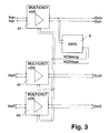
- the proportionate power loss of the control circuit 5 per LVDS buffer can be reduced in that, in addition to the buffer shown in FIG. 2, which is designated in FIG. 3 with the reference number 41, further LVDS buffers 42 and 43 from the Control circuit 5 of the first buffer 41 can also be controlled (not regulated).
- the control inputs VCSwing and VCOffset are led to gates of MOSFETs and therefore no input current flows.
- the further buffers 42 and 43 are also contained in an integrated circuit which contains an arrangement according to FIG. 2. Instead, they can be arranged separately.
- the output stage is a current negative feedback Differential stage executed by connecting the emitters of transistors Q1 and Q2 are.
- a further reduction in power loss is achieved by the
- the default value of the amplitude reference value is reduced to such an extent that the specified amplitude value of 250mV under all technology and Environmental conditions are still observed. This is particularly due to the existing regulation supports.
- the arrangement according to FIG. 2 is integrated in BiCMOS technology Circuit realized. They are namely bipolar transistors and at least one N-channel MOSFET (Transistor N1) and at least one P-channel MOSFET (transistor P1) available. Instead, two could also be used for the MOSFETs there Equipolar MOSFETs (two with N-channel or two with P-channel) can be provided. In this latter case, the specific circuit must generally be modified For example, the MOSFET must now be in a different polarity to be provided, in the current path that it controls, to another place be relocated. In comparison to the arrangement according to FIG. 2, it can also the polarity of one of those coming from the control block may be required Reverse control signals.
Landscapes
- Engineering & Computer Science (AREA)
- Power Engineering (AREA)
- Amplifiers (AREA)
- Logic Circuits (AREA)
- Metal-Oxide And Bipolar Metal-Oxide Semiconductor Integrated Circuits (AREA)
Abstract
Description
eine Multipliziererschaltung mit einer Ausgangsstufe des LVDS-Treibers verbunden ist, und dass die Multipliziererschaltung mittels einer Regelungsschaltung gesteuert wird, die Steuersignale zum Steuern einer Stromquelle der Multipliziererschaltung und zum Steuern des Verstärkungsfaktors von differenziellen Eingangssignalen der Multipliziererschaltung erzeugt.
Das differentielle Dateneingangssignal wird an den Knoten Inp+ bzw. Inp- der beiden unteren Transistoren QP5 bzw. QP6 des Vierquadranten Steilheitsmultiplizierers angelegt. Die Transistoren QP5 und QP6 bilden einen Differenzverstärker. Die Kollektoren dieser Transistoren funktionieren als Ausgänge von zwei Stromquellen, die durch das differentielle Dateneingangssignal 180 Grad phasenversetzt zueinander arbeiten.
Der Gesamtstrom des regelbaren Verstärkers wird durch die regelbare Stromquelle 15 bereit gestellt. Diese besteht aus Transistor QP8, dessen Emitter über Widerstand RP7 gegengekoppelt ist. Das Basispotential an QP8 wird über den Transistor P1 bereitgestellt dessen Eingang durch die Regelspannung VCOffset gesteuert wird.
Die Transistoren QP1, QP2, QP3 und QP4 sind die eigentlichen Stellglieder des regelbaren Verstärkers. Die Eingänge von QP1/QP4 bzw. QP2/QP3 sind zusammengefasst und dienen als Steuereingänge des regelbaren Verstärkers. Die Kollektoren von QP2/QP4 sind an Kollektorwiderstand RP3 und die Kollektoren von QP1/QP3 sind an Kollektorwiderstand RP2 angeschlossen. Die an die Widerstände RP2 und RP3 angeschlossenen Kollektoren bilden die Ausgänge der Multipliziererschaltung und liefern gegenphasige Signale (Gegentaktsignal oder differentielles Signal) auf einem Niveau größer als Null Volt an die Eingänge der Ausgangsstufe 3. RP1 dient zur Spannungsabsenkung, um eine Sättigung der Kollektoren der Transistoren Q1 und Q2 in der Ausgangsstufe 3 zu verhindern und verbessert das dynamische Verhalten der Ausgangsstufe 3.
Der Steuereingang am Transistorpaar QP2/QP3 hat über Widerstand RP5 ein festes Potential. Das Potential am Steuereingang des Transistorpaares QP1/QP4 wird durch einen veränderlichen Spannungsteiler, bestehend aus Widerstand RP4 und Transistor N1, bereitgestellt. Das Teilerverhältnis des Spannungsteilers wird durch die Regelspannung VCSwing bestimmt.
Durch den Wert der Regelspannung am Eingang QP1 /QP4 gegenüber der Festspannung am Eingang QP2/QP3 wird der Stromfluss durch diese Transistoren bestimmt. Je nach Steuerspannung am Eingang QP1/QP4 findet eine Addition der 180 Grad phasenversetzten Ströme durch QP2 und QP4 bzw. durch QP1 und QP3 statt. Dadurch kann die Spannungsamplitude an RP2 und RP3 verändert werden. Ist die Spannung an den beiden Steuereingängen gleich, ist die Summe der Teilströme zu jedem Zeitpunkt gleich und damit die Verstärkung 0. Sind beide Spannungen an den Steuereingängen ungleich, ist die Verstärkung ungleich 0.
Dabei darf die Spannung am Steuereingang QP1/QP4 nie kleiner als die Spannung am Steuereingang QP3/QP4 werden, da sonst eine Phasendrehung des Datensignals erfolgt. Dies wird durch eine geeignet Dimensionierung verhindert.
Durch das etwas erhöhte Potential am Eingang QP1/QP4 gegenüber der Festspannung am Eingang QP2/QP3 verringert sich die Differenzspannung an diesem Eingang des Multiplizierers und damit der Multiplikationsfaktor, was zu einer Verringerung der Spannungsamplitude an den Widerständen RP2 und RP3 und folglich auch zur Verringerung der Amplitude am Ausgang der L VDS-Treiberschaltung führt, da diese eine fest eingestellte Verstärkung hat.
Gemäß Figur 3 läßt sich die anteilige Verlustleistung der Regelschaltung 5 pro LVDS-Buffer dadurch reduzieren, indem zusätzlich zu dem in Fig. 2 gezeigten Buffer, der in Fig. 3 mit dem Bezugszeichen 41 bezeichnet ist, weitere LVDS-Buffer 42 und 43 von der Regelschaltung 5 des ersten Buffers 41 mitgesteuert (nicht geregelt) werden. Diese Anschaltung der weiteren Buffer ist ohne Änderungen möglich, weil die Regeleingänge VCSwing und VCOffset auf Gates von MOSFETs geführt sind und dadurch kein Eingangsstrom fließt. Im Beispiel sind die weiteren Buffer 42 und 43 in einer integrierten Schaltung, die eine Anordnung nach Fig. 2 enthält, mit enthalten. Sie können statt dessen separat angeordnet sein.
Claims (8)
- Schaltungsanordnung für einen LVDS-Treiber (LVDS = Low Voltage Differential Signal), die eine kombinierte bipolare und MOSFET-Technologie mit mindestens zwei MOSFETs verwendet,
dadurch gekennzeichnet, dass
eine Multipliziererschaltung (11) mit einer Ausgangsstufe (3) des LVDS-Treibers (1) verbunden ist, und dass die Multipliziererschaltung mittels einer Regelungsschaltung (5) gesteuert ist, die Steuersignale zum Steuern einer Stromquelle der Multipliziererschaltung und zum Steuern des Verstärkungsfaktors von differenziellen Eingangssignalen der Multipliziererschaltung erzeugt. - Schaltungsanordnung nach Anspruch 1, dadurch gekennzeichnet, dass die Ausgangsstufe für die Speisung ausschließlich durch eine erste Betriebsspannung gegenüber Masse ausgebildet ist, und dass mindestens eine weitere Komponente der Schaltung zur Speisung mit Hilfe einer zweiten, gegenüber der ersten Betriebsspannung gegenpoligen Betriebsspannung ausgebildet ist.
- Schaltungsanordnung nach Anspruch 2, dadurch gekennzeichnet, dass die Multipliziererschaltung (11) zur Speisung gleichzeitig durch die erste und die zweite Betriebsspannung ausgebildet ist.
- Schaltungsanordnung nach Anspruch 1, dadurch gekennzeichnet, dass die Steuersignalausgänge der Regelungsschaltung (5) mit je einem Eingang eines MOSFET gekoppelt sind, wobei einer der genannten MOSFETs zur Steuerung der Stromquelle ausgebildet ist, und der andere MOSFET zur Steuerung des Verstärkungsfaktors des Multiplizierers ausgebildet ist.
- Schaltungsanordnung nach Anspruch 1, dadurch gekennzeichnet, dass die Stromquelle zur Veränderung des Offset der Ausgangsspannung des LVDS-Treibers vorgesehen ist.
- Schaltungsanordnung nach Anspruch 1, dadurch gekennzeichnet, dass die Multipliziererschaltung zur Lieferung zweier gegenphasiger zu verstärkender Signale an die Ausgangsstufe ausgebildet ist.
- Schaltungsanordnung nach Anspruch 6, dadurch gekennzeichnet, dass die Ausgangsstufe bipolare Transistoren enthält, die jeweils zur Verstärkung eines der Ausgangssignale des Multiplizierers ausgebildet sind.
- Schaltungsanordnung nach Anspruch 1, dadurch gekennzeichnet, dass die Regelungsschaltung eine Einrichtung zum Ermitteln einer von der Spannungsdifferenz zwischen von der Ausgangsstufe gelieferten differentiellen Signalen abhängigen Steuersignals und eine Einrichtung zum Erzeugen eines vom Offset der Ausgangssignale der Ausgangsstufe abhängigen Steuersignals ausgebildet ist.
Priority Applications (4)
| Application Number | Priority Date | Filing Date | Title |
|---|---|---|---|
| EP02360166A EP1369993B1 (de) | 2002-06-07 | 2002-06-07 | LVSD-Treiber in bipolarer und MOS-Technologie |
| DE50204866T DE50204866D1 (de) | 2002-06-07 | 2002-06-07 | LVSD-Treiber in bipolarer und MOS-Technologie |
| AT02360166T ATE309640T1 (de) | 2002-06-07 | 2002-06-07 | Lvsd-treiber in bipolarer und mos-technologie |
| US10/435,389 US6791377B2 (en) | 2002-06-07 | 2003-05-12 | LVDS driver in bipolar and MOS technology |
Applications Claiming Priority (1)
| Application Number | Priority Date | Filing Date | Title |
|---|---|---|---|
| EP02360166A EP1369993B1 (de) | 2002-06-07 | 2002-06-07 | LVSD-Treiber in bipolarer und MOS-Technologie |
Publications (2)
| Publication Number | Publication Date |
|---|---|
| EP1369993A1 true EP1369993A1 (de) | 2003-12-10 |
| EP1369993B1 EP1369993B1 (de) | 2005-11-09 |
Family
ID=29433225
Family Applications (1)
| Application Number | Title | Priority Date | Filing Date |
|---|---|---|---|
| EP02360166A Expired - Lifetime EP1369993B1 (de) | 2002-06-07 | 2002-06-07 | LVSD-Treiber in bipolarer und MOS-Technologie |
Country Status (4)
| Country | Link |
|---|---|
| US (1) | US6791377B2 (de) |
| EP (1) | EP1369993B1 (de) |
| AT (1) | ATE309640T1 (de) |
| DE (1) | DE50204866D1 (de) |
Families Citing this family (52)
| Publication number | Priority date | Publication date | Assignee | Title |
|---|---|---|---|---|
| US8103496B1 (en) | 2000-10-26 | 2012-01-24 | Cypress Semicondutor Corporation | Breakpoint control in an in-circuit emulation system |
| US8160864B1 (en) | 2000-10-26 | 2012-04-17 | Cypress Semiconductor Corporation | In-circuit emulator and pod synchronized boot |
| US8176296B2 (en) | 2000-10-26 | 2012-05-08 | Cypress Semiconductor Corporation | Programmable microcontroller architecture |
| US8149048B1 (en) | 2000-10-26 | 2012-04-03 | Cypress Semiconductor Corporation | Apparatus and method for programmable power management in a programmable analog circuit block |
| US6724220B1 (en) | 2000-10-26 | 2004-04-20 | Cyress Semiconductor Corporation | Programmable microcontroller architecture (mixed analog/digital) |
| US7765095B1 (en) | 2000-10-26 | 2010-07-27 | Cypress Semiconductor Corporation | Conditional branching in an in-circuit emulation system |
| US6943591B1 (en) * | 2001-08-17 | 2005-09-13 | National Semiconductor Corporation | Apparatus and method for detecting a fault condition in a common-mode signal |
| US7406674B1 (en) | 2001-10-24 | 2008-07-29 | Cypress Semiconductor Corporation | Method and apparatus for generating microcontroller configuration information |
| US8078970B1 (en) | 2001-11-09 | 2011-12-13 | Cypress Semiconductor Corporation | Graphical user interface with user-selectable list-box |
| US8042093B1 (en) | 2001-11-15 | 2011-10-18 | Cypress Semiconductor Corporation | System providing automatic source code generation for personalization and parameterization of user modules |
| US7844437B1 (en) | 2001-11-19 | 2010-11-30 | Cypress Semiconductor Corporation | System and method for performing next placements and pruning of disallowed placements for programming an integrated circuit |
| US8069405B1 (en) | 2001-11-19 | 2011-11-29 | Cypress Semiconductor Corporation | User interface for efficiently browsing an electronic document using data-driven tabs |
| US7770113B1 (en) | 2001-11-19 | 2010-08-03 | Cypress Semiconductor Corporation | System and method for dynamically generating a configuration datasheet |
| US7774190B1 (en) | 2001-11-19 | 2010-08-10 | Cypress Semiconductor Corporation | Sleep and stall in an in-circuit emulation system |
| US6971004B1 (en) | 2001-11-19 | 2005-11-29 | Cypress Semiconductor Corp. | System and method of dynamically reconfiguring a programmable integrated circuit |
| US8103497B1 (en) | 2002-03-28 | 2012-01-24 | Cypress Semiconductor Corporation | External interface for event architecture |
| US7308608B1 (en) | 2002-05-01 | 2007-12-11 | Cypress Semiconductor Corporation | Reconfigurable testing system and method |
| US7761845B1 (en) | 2002-09-09 | 2010-07-20 | Cypress Semiconductor Corporation | Method for parameterizing a user module |
| US7068077B1 (en) | 2003-04-17 | 2006-06-27 | Cypress Semiconductor Corporation | LVDS output driver having low supply voltage capability |
| US7088166B1 (en) * | 2003-06-19 | 2006-08-08 | Cypress Semiconductor Corporation | LVDS input circuit with extended common mode range |
| US7098700B2 (en) * | 2003-12-12 | 2006-08-29 | Telasic Communications, Inc. | Low power output driver |
| US7295049B1 (en) | 2004-03-25 | 2007-11-13 | Cypress Semiconductor Corporation | Method and circuit for rapid alignment of signals |
| KR100559378B1 (ko) * | 2004-07-02 | 2006-03-10 | 삼성전자주식회사 | 동작 주파수에 따라 소모 전류를 제어하는 저전압 차동신호 방식 수신 장치 및 그 동작 방법 |
| US8286125B2 (en) | 2004-08-13 | 2012-10-09 | Cypress Semiconductor Corporation | Model for a hardware device-independent method of defining embedded firmware for programmable systems |
| US8069436B2 (en) | 2004-08-13 | 2011-11-29 | Cypress Semiconductor Corporation | Providing hardware independence to automate code generation of processing device firmware |
| US7332976B1 (en) | 2005-02-04 | 2008-02-19 | Cypress Semiconductor Corporation | Poly-phase frequency synthesis oscillator |
| US7400183B1 (en) | 2005-05-05 | 2008-07-15 | Cypress Semiconductor Corporation | Voltage controlled oscillator delay cell and method |
| US8089461B2 (en) | 2005-06-23 | 2012-01-03 | Cypress Semiconductor Corporation | Touch wake for electronic devices |
| US8085067B1 (en) | 2005-12-21 | 2011-12-27 | Cypress Semiconductor Corporation | Differential-to-single ended signal converter circuit and method |
| US8067948B2 (en) | 2006-03-27 | 2011-11-29 | Cypress Semiconductor Corporation | Input/output multiplexer bus |
| KR100874700B1 (ko) | 2006-12-06 | 2008-12-18 | 한국전자통신연구원 | 바이폴라 트랜지스터의 제조 방법 및 이를 이용한 고속저전압 차동 신호 구동기 |
| US20080136464A1 (en) * | 2006-12-06 | 2008-06-12 | Electronics And Telecommunications Research Institute | Method of fabricating bipolar transistors and high-speed lvds driver with the bipolar transistors |
| US8092083B2 (en) | 2007-04-17 | 2012-01-10 | Cypress Semiconductor Corporation | Temperature sensor with digital bandgap |
| US9564902B2 (en) | 2007-04-17 | 2017-02-07 | Cypress Semiconductor Corporation | Dynamically configurable and re-configurable data path |
| US8516025B2 (en) | 2007-04-17 | 2013-08-20 | Cypress Semiconductor Corporation | Clock driven dynamic datapath chaining |
| US8130025B2 (en) | 2007-04-17 | 2012-03-06 | Cypress Semiconductor Corporation | Numerical band gap |
| US8040266B2 (en) | 2007-04-17 | 2011-10-18 | Cypress Semiconductor Corporation | Programmable sigma-delta analog-to-digital converter |
| US7737724B2 (en) | 2007-04-17 | 2010-06-15 | Cypress Semiconductor Corporation | Universal digital block interconnection and channel routing |
| US8026739B2 (en) | 2007-04-17 | 2011-09-27 | Cypress Semiconductor Corporation | System level interconnect with programmable switching |
| US9720805B1 (en) | 2007-04-25 | 2017-08-01 | Cypress Semiconductor Corporation | System and method for controlling a target device |
| US8065653B1 (en) | 2007-04-25 | 2011-11-22 | Cypress Semiconductor Corporation | Configuration of programmable IC design elements |
| US8266575B1 (en) | 2007-04-25 | 2012-09-11 | Cypress Semiconductor Corporation | Systems and methods for dynamically reconfiguring a programmable system on a chip |
| US8049569B1 (en) | 2007-09-05 | 2011-11-01 | Cypress Semiconductor Corporation | Circuit and method for improving the accuracy of a crystal-less oscillator having dual-frequency modes |
| US7777531B2 (en) * | 2007-10-30 | 2010-08-17 | Texas Instruments Incorporated | Low power low voltage differential signaling (LVDS) output drivers |
| US7974589B2 (en) * | 2008-02-13 | 2011-07-05 | Analog Devices, Inc. | High-speed data transmitters |
| US9448964B2 (en) | 2009-05-04 | 2016-09-20 | Cypress Semiconductor Corporation | Autonomous control in a programmable system |
| WO2011033708A1 (ja) * | 2009-09-18 | 2011-03-24 | パナソニック株式会社 | ドライバ回路および映像システム |
| US7944252B1 (en) * | 2009-11-05 | 2011-05-17 | Texas Instruments Incorporated | High performance LVDS driver for scalable supply |
| US8331865B2 (en) * | 2009-11-18 | 2012-12-11 | Motorola Solutions, Inc. | High speed minimal interference adaptive tranceiver interface and method thereof |
| US8049534B2 (en) * | 2010-02-15 | 2011-11-01 | Texas Instruments Incorporated | Low-power high-speed differential driver with precision current steering |
| US10057523B1 (en) | 2017-02-13 | 2018-08-21 | Alexander Krymski | Image sensors and methods with multiple phase-locked loops and serializers |
| CN119696598B (zh) * | 2024-12-03 | 2025-09-23 | 电子科技大学 | 一种带压摆控制的lvds发送器 |
Citations (4)
| Publication number | Priority date | Publication date | Assignee | Title |
|---|---|---|---|---|
| US4471320A (en) * | 1981-05-27 | 1984-09-11 | Frey Douglas R | Voltage controlled element |
| EP0831480A1 (de) * | 1996-09-24 | 1998-03-25 | Hewlett-Packard Company | Datenverabeitungsgerät und -verfahren |
| US6040731A (en) * | 1997-05-01 | 2000-03-21 | Raytheon Company | Differential pair gain control stage |
| US6111431A (en) * | 1998-05-14 | 2000-08-29 | National Semiconductor Corporation | LVDS driver for backplane applications |
Family Cites Families (3)
| Publication number | Priority date | Publication date | Assignee | Title |
|---|---|---|---|---|
| US4999519A (en) * | 1987-12-04 | 1991-03-12 | Hitachi Vlsi Engineering Corporation | Semiconductor circuit with low power consumption having emitter-coupled logic or differential amplifier |
| US5151625A (en) * | 1990-11-08 | 1992-09-29 | The Ohio State University | High frequency BiMOS linear V-I converter, voltage multiplier, mixer |
| US5418497A (en) * | 1994-07-05 | 1995-05-23 | Motorola, Inc. | Low voltage VCO having two oscillator circuits of different frequencies |
-
2002
- 2002-06-07 DE DE50204866T patent/DE50204866D1/de not_active Expired - Fee Related
- 2002-06-07 AT AT02360166T patent/ATE309640T1/de not_active IP Right Cessation
- 2002-06-07 EP EP02360166A patent/EP1369993B1/de not_active Expired - Lifetime
-
2003
- 2003-05-12 US US10/435,389 patent/US6791377B2/en not_active Expired - Fee Related
Patent Citations (4)
| Publication number | Priority date | Publication date | Assignee | Title |
|---|---|---|---|---|
| US4471320A (en) * | 1981-05-27 | 1984-09-11 | Frey Douglas R | Voltage controlled element |
| EP0831480A1 (de) * | 1996-09-24 | 1998-03-25 | Hewlett-Packard Company | Datenverabeitungsgerät und -verfahren |
| US6040731A (en) * | 1997-05-01 | 2000-03-21 | Raytheon Company | Differential pair gain control stage |
| US6111431A (en) * | 1998-05-14 | 2000-08-29 | National Semiconductor Corporation | LVDS driver for backplane applications |
Non-Patent Citations (2)
| Title |
|---|
| REIN H-M ET AL: "DESIGN CONSIDERATIONS FOR VERY-HIGH-SPEED SI-BIPOLAR IC'S OPERATINGUP TO 50 GB/S", IEEE JOURNAL OF SOLID-STATE CIRCUITS, IEEE INC. NEW YORK, US, vol. 31, no. 8, 1 August 1996 (1996-08-01), pages 1076 - 1090, XP000623557, ISSN: 0018-9200 * |
| VREEDE DE L C N ET AL: "A HIGH GAIN SILICON AGC AMPLIFIER WITH A 3 DB BANDWIDTH OF 4 GHZ", IEEE TRANSACTIONS ON MICROWAVE THEORY AND TECHNIQUES, IEEE INC. NEW YORK, US, vol. 42, no. 4, PART 1, 1 April 1994 (1994-04-01), pages 546 - 551, XP000442444, ISSN: 0018-9480 * |
Also Published As
| Publication number | Publication date |
|---|---|
| US20030227303A1 (en) | 2003-12-11 |
| US6791377B2 (en) | 2004-09-14 |
| ATE309640T1 (de) | 2005-11-15 |
| EP1369993B1 (de) | 2005-11-09 |
| DE50204866D1 (de) | 2005-12-15 |
Similar Documents
| Publication | Publication Date | Title |
|---|---|---|
| EP1369993B1 (de) | LVSD-Treiber in bipolarer und MOS-Technologie | |
| DE69838633T2 (de) | Konstantstrom-CMOS-Ausgangstreiberschaltung mit Dual-Gate-Transistoren | |
| DE102009054113B4 (de) | Prozess-, Spannungs- und Temperaturregelung für Hochgeschwindigkeits-Verstärker mit festem Verstärkungsgrad sowie mit variabler Verstärkung und geringem Stromverbrauch auf der Basis von MOSFET-Widerständen | |
| DE3523400C2 (de) | Schaltungsanordnung für eine Ausgangsstufe der Klasse AB mit großer Schwingungsweite | |
| DE102014118167B4 (de) | Analogschalter und Verfahren zum Steuern von Analogschaltern | |
| DE3852930T2 (de) | Gefalteter Kaskodenverstärker mit über den ganzen Betriebsspannungsbereich gehenden Gleichtaktbereich. | |
| DE69522150T2 (de) | Operationsverstärker und Stromdetektorschaltungen | |
| DE69730724T2 (de) | Leistungsendstufenschaltung mit niedriger impedanz sowie verfahren | |
| DE69428045T2 (de) | Programmierbarer cmos bus- und übertragungsleitungstreiber | |
| DE112012003708T5 (de) | Vierquadranten-Schaltung mit Bootstrap-Ansteuerung | |
| DE19922354A1 (de) | LVDS-Treiber für Backplane-Anwendungen | |
| EP1269625A1 (de) | Elektronische ausgangsstufe | |
| DE69612007T2 (de) | Ausgangspuffer mit gemeinsam genutzten zwischenknoten | |
| DE102005039114A1 (de) | Spannungsregler mit einem geringen Spannungsabfall | |
| DE69937428T2 (de) | Gleichtaktrückkopplungsschaltung und Verfahren | |
| DE3832448A1 (de) | Messverstaerker mit programmierbarer verstaerkung | |
| DE60318103T2 (de) | Einschalten eines bustreibers mit gesteuerter anstiegszeit | |
| EP0730214B1 (de) | Stromspiegel in MOS-Technik mit weit aussteuerbaren Kaskodestufen | |
| EP0763916A2 (de) | Empfängerschaltung mit konstantem Eingangswiderstand | |
| DE102008047903A1 (de) | Integrierte Schaltung und Verfahren zur Erzeugung eines Vorspannungssignals für einen Datensignalempfänger | |
| DE19533768C1 (de) | Stromtreiberschaltung mit Querstromregelung | |
| DE102021106859B4 (de) | Komparator mit konfigurierbaren betriebsmodi | |
| DE68927715T2 (de) | Nichtlinearer Verstärker | |
| DE69223752T2 (de) | Halbleiterschaltungen | |
| EP0642217B1 (de) | Gegentaktendstufe mit einer Einstellung des Querstroms der Gegentaktendstufe |
Legal Events
| Date | Code | Title | Description |
|---|---|---|---|
| PUAI | Public reference made under article 153(3) epc to a published international application that has entered the european phase |
Free format text: ORIGINAL CODE: 0009012 |
|
| 17P | Request for examination filed |
Effective date: 20030219 |
|
| AK | Designated contracting states |
Kind code of ref document: A1 Designated state(s): AT BE CH CY DE DK ES FI FR GB GR IE IT LI LU MC NL PT SE TR |
|
| AX | Request for extension of the european patent |
Extension state: AL LT LV MK RO SI |
|
| AKX | Designation fees paid |
Designated state(s): AT BE CH CY DE DK ES FI FR GB GR IE IT LI LU MC NL PT SE TR |
|
| GRAP | Despatch of communication of intention to grant a patent |
Free format text: ORIGINAL CODE: EPIDOSNIGR1 |
|
| RIN1 | Information on inventor provided before grant (corrected) |
Inventor name: ROESENER, DETLEF Inventor name: ILCHMANN, FRANK Inventor name: BALLENTIN, RALPH |
|
| GRAS | Grant fee paid |
Free format text: ORIGINAL CODE: EPIDOSNIGR3 |
|
| GRAA | (expected) grant |
Free format text: ORIGINAL CODE: 0009210 |
|
| AK | Designated contracting states |
Kind code of ref document: B1 Designated state(s): AT BE CH CY DE DK ES FI FR GB GR IE IT LI LU MC NL PT SE TR |
|
| PG25 | Lapsed in a contracting state [announced via postgrant information from national office to epo] |
Ref country code: NL Free format text: LAPSE BECAUSE OF FAILURE TO SUBMIT A TRANSLATION OF THE DESCRIPTION OR TO PAY THE FEE WITHIN THE PRESCRIBED TIME-LIMIT Effective date: 20051109 Ref country code: IE Free format text: LAPSE BECAUSE OF FAILURE TO SUBMIT A TRANSLATION OF THE DESCRIPTION OR TO PAY THE FEE WITHIN THE PRESCRIBED TIME-LIMIT Effective date: 20051109 Ref country code: FI Free format text: LAPSE BECAUSE OF FAILURE TO SUBMIT A TRANSLATION OF THE DESCRIPTION OR TO PAY THE FEE WITHIN THE PRESCRIBED TIME-LIMIT Effective date: 20051109 |
|
| REG | Reference to a national code |
Ref country code: GB Ref legal event code: FG4D Free format text: NOT ENGLISH |
|
| REG | Reference to a national code |
Ref country code: CH Ref legal event code: EP |
|
| GBT | Gb: translation of ep patent filed (gb section 77(6)(a)/1977) |
Effective date: 20051109 |
|
| REG | Reference to a national code |
Ref country code: IE Ref legal event code: FG4D Free format text: LANGUAGE OF EP DOCUMENT: GERMAN |
|
| REF | Corresponds to: |
Ref document number: 50204866 Country of ref document: DE Date of ref document: 20051215 Kind code of ref document: P |
|
| PG25 | Lapsed in a contracting state [announced via postgrant information from national office to epo] |
Ref country code: SE Free format text: LAPSE BECAUSE OF FAILURE TO SUBMIT A TRANSLATION OF THE DESCRIPTION OR TO PAY THE FEE WITHIN THE PRESCRIBED TIME-LIMIT Effective date: 20060209 Ref country code: GR Free format text: LAPSE BECAUSE OF FAILURE TO SUBMIT A TRANSLATION OF THE DESCRIPTION OR TO PAY THE FEE WITHIN THE PRESCRIBED TIME-LIMIT Effective date: 20060209 Ref country code: DK Free format text: LAPSE BECAUSE OF FAILURE TO SUBMIT A TRANSLATION OF THE DESCRIPTION OR TO PAY THE FEE WITHIN THE PRESCRIBED TIME-LIMIT Effective date: 20060209 |
|
| PG25 | Lapsed in a contracting state [announced via postgrant information from national office to epo] |
Ref country code: ES Free format text: LAPSE BECAUSE OF FAILURE TO SUBMIT A TRANSLATION OF THE DESCRIPTION OR TO PAY THE FEE WITHIN THE PRESCRIBED TIME-LIMIT Effective date: 20060220 |
|
| PG25 | Lapsed in a contracting state [announced via postgrant information from national office to epo] |
Ref country code: PT Free format text: LAPSE BECAUSE OF FAILURE TO SUBMIT A TRANSLATION OF THE DESCRIPTION OR TO PAY THE FEE WITHIN THE PRESCRIBED TIME-LIMIT Effective date: 20060410 |
|
| NLV1 | Nl: lapsed or annulled due to failure to fulfill the requirements of art. 29p and 29m of the patents act | ||
| ET | Fr: translation filed | ||
| REG | Reference to a national code |
Ref country code: IE Ref legal event code: FD4D |
|
| PG25 | Lapsed in a contracting state [announced via postgrant information from national office to epo] |
Ref country code: LI Free format text: LAPSE BECAUSE OF NON-PAYMENT OF DUE FEES Effective date: 20060630 Ref country code: CH Free format text: LAPSE BECAUSE OF NON-PAYMENT OF DUE FEES Effective date: 20060630 Ref country code: BE Free format text: LAPSE BECAUSE OF NON-PAYMENT OF DUE FEES Effective date: 20060630 Ref country code: MC Free format text: LAPSE BECAUSE OF NON-PAYMENT OF DUE FEES Effective date: 20060630 |
|
| PLBE | No opposition filed within time limit |
Free format text: ORIGINAL CODE: 0009261 |
|
| STAA | Information on the status of an ep patent application or granted ep patent |
Free format text: STATUS: NO OPPOSITION FILED WITHIN TIME LIMIT |
|
| 26N | No opposition filed |
Effective date: 20060810 |
|
| REG | Reference to a national code |
Ref country code: CH Ref legal event code: PL |
|
| PGFP | Annual fee paid to national office [announced via postgrant information from national office to epo] |
Ref country code: DE Payment date: 20070622 Year of fee payment: 6 |
|
| PG25 | Lapsed in a contracting state [announced via postgrant information from national office to epo] |
Ref country code: AT Free format text: LAPSE BECAUSE OF NON-PAYMENT OF DUE FEES Effective date: 20060607 |
|
| PGFP | Annual fee paid to national office [announced via postgrant information from national office to epo] |
Ref country code: GB Payment date: 20070621 Year of fee payment: 6 |
|
| BERE | Be: lapsed |
Owner name: ALCATEL Effective date: 20060630 |
|
| PGFP | Annual fee paid to national office [announced via postgrant information from national office to epo] |
Ref country code: IT Payment date: 20070623 Year of fee payment: 6 |
|
| PGFP | Annual fee paid to national office [announced via postgrant information from national office to epo] |
Ref country code: FR Payment date: 20070615 Year of fee payment: 6 |
|
| PG25 | Lapsed in a contracting state [announced via postgrant information from national office to epo] |
Ref country code: TR Free format text: LAPSE BECAUSE OF FAILURE TO SUBMIT A TRANSLATION OF THE DESCRIPTION OR TO PAY THE FEE WITHIN THE PRESCRIBED TIME-LIMIT Effective date: 20051109 Ref country code: LU Free format text: LAPSE BECAUSE OF NON-PAYMENT OF DUE FEES Effective date: 20060607 |
|
| PG25 | Lapsed in a contracting state [announced via postgrant information from national office to epo] |
Ref country code: CY Free format text: LAPSE BECAUSE OF FAILURE TO SUBMIT A TRANSLATION OF THE DESCRIPTION OR TO PAY THE FEE WITHIN THE PRESCRIBED TIME-LIMIT Effective date: 20051109 |
|
| GBPC | Gb: european patent ceased through non-payment of renewal fee |
Effective date: 20080607 |
|
| REG | Reference to a national code |
Ref country code: FR Ref legal event code: ST Effective date: 20090228 |
|
| PG25 | Lapsed in a contracting state [announced via postgrant information from national office to epo] |
Ref country code: DE Free format text: LAPSE BECAUSE OF NON-PAYMENT OF DUE FEES Effective date: 20090101 |
|
| PG25 | Lapsed in a contracting state [announced via postgrant information from national office to epo] |
Ref country code: GB Free format text: LAPSE BECAUSE OF NON-PAYMENT OF DUE FEES Effective date: 20080607 |
|
| PG25 | Lapsed in a contracting state [announced via postgrant information from national office to epo] |
Ref country code: IT Free format text: LAPSE BECAUSE OF NON-PAYMENT OF DUE FEES Effective date: 20080607 Ref country code: FR Free format text: LAPSE BECAUSE OF NON-PAYMENT OF DUE FEES Effective date: 20080630 |