EP1367676A1 - Vorrichtung mit organischen lichtemittierenden Dioden mit einem flexiblen Substrat auf einem Träger - Google Patents
Vorrichtung mit organischen lichtemittierenden Dioden mit einem flexiblen Substrat auf einem Träger Download PDFInfo
- Publication number
- EP1367676A1 EP1367676A1 EP20030076478 EP03076478A EP1367676A1 EP 1367676 A1 EP1367676 A1 EP 1367676A1 EP 20030076478 EP20030076478 EP 20030076478 EP 03076478 A EP03076478 A EP 03076478A EP 1367676 A1 EP1367676 A1 EP 1367676A1
- Authority
- EP
- European Patent Office
- Prior art keywords
- oled
- layer
- light source
- electrodes
- flexible substrate
- Prior art date
- Legal status (The legal status is an assumption and is not a legal conclusion. Google has not performed a legal analysis and makes no representation as to the accuracy of the status listed.)
- Granted
Links
Images


Classifications
-
- H—ELECTRICITY
- H01—ELECTRIC ELEMENTS
- H01R—ELECTRICALLY-CONDUCTIVE CONNECTIONS; STRUCTURAL ASSOCIATIONS OF A PLURALITY OF MUTUALLY-INSULATED ELECTRICAL CONNECTING ELEMENTS; COUPLING DEVICES; CURRENT COLLECTORS
- H01R12/00—Structural associations of a plurality of mutually-insulated electrical connecting elements, specially adapted for printed circuits, e.g. printed circuit boards [PCB], flat or ribbon cables, or like generally planar structures, e.g. terminal strips, terminal blocks; Coupling devices specially adapted for printed circuits, flat or ribbon cables, or like generally planar structures; Terminals specially adapted for contact with, or insertion into, printed circuits, flat or ribbon cables, or like generally planar structures
- H01R12/70—Coupling devices
- H01R12/7076—Coupling devices for connection between PCB and component, e.g. display
-
- H—ELECTRICITY
- H05—ELECTRIC TECHNIQUES NOT OTHERWISE PROVIDED FOR
- H05B—ELECTRIC HEATING; ELECTRIC LIGHT SOURCES NOT OTHERWISE PROVIDED FOR; CIRCUIT ARRANGEMENTS FOR ELECTRIC LIGHT SOURCES, IN GENERAL
- H05B33/00—Electroluminescent light sources
-
- F—MECHANICAL ENGINEERING; LIGHTING; HEATING; WEAPONS; BLASTING
- F21—LIGHTING
- F21K—NON-ELECTRIC LIGHT SOURCES USING LUMINESCENCE; LIGHT SOURCES USING ELECTROCHEMILUMINESCENCE; LIGHT SOURCES USING CHARGES OF COMBUSTIBLE MATERIAL; LIGHT SOURCES USING SEMICONDUCTOR DEVICES AS LIGHT-GENERATING ELEMENTS; LIGHT SOURCES NOT OTHERWISE PROVIDED FOR
- F21K9/00—Light sources using semiconductor devices as light-generating elements, e.g. using light-emitting diodes [LED] or lasers
- F21K9/20—Light sources comprising attachment means
- F21K9/23—Retrofit light sources for lighting devices with a single fitting for each light source, e.g. for substitution of incandescent lamps with bayonet or threaded fittings
-
- F—MECHANICAL ENGINEERING; LIGHTING; HEATING; WEAPONS; BLASTING
- F21—LIGHTING
- F21V—FUNCTIONAL FEATURES OR DETAILS OF LIGHTING DEVICES OR SYSTEMS THEREOF; STRUCTURAL COMBINATIONS OF LIGHTING DEVICES WITH OTHER ARTICLES, NOT OTHERWISE PROVIDED FOR
- F21V3/00—Globes; Bowls; Cover glasses
-
- F—MECHANICAL ENGINEERING; LIGHTING; HEATING; WEAPONS; BLASTING
- F21—LIGHTING
- F21Y—INDEXING SCHEME ASSOCIATED WITH SUBCLASSES F21K, F21L, F21S and F21V, RELATING TO THE FORM OR THE KIND OF THE LIGHT SOURCES OR OF THE COLOUR OF THE LIGHT EMITTED
- F21Y2105/00—Planar light sources
-
- F—MECHANICAL ENGINEERING; LIGHTING; HEATING; WEAPONS; BLASTING
- F21—LIGHTING
- F21Y—INDEXING SCHEME ASSOCIATED WITH SUBCLASSES F21K, F21L, F21S and F21V, RELATING TO THE FORM OR THE KIND OF THE LIGHT SOURCES OR OF THE COLOUR OF THE LIGHT EMITTED
- F21Y2115/00—Light-generating elements of semiconductor light sources
- F21Y2115/10—Light-emitting diodes [LED]
- F21Y2115/15—Organic light-emitting diodes [OLED]
-
- H—ELECTRICITY
- H01—ELECTRIC ELEMENTS
- H01R—ELECTRICALLY-CONDUCTIVE CONNECTIONS; STRUCTURAL ASSOCIATIONS OF A PLURALITY OF MUTUALLY-INSULATED ELECTRICAL CONNECTING ELEMENTS; COUPLING DEVICES; CURRENT COLLECTORS
- H01R13/00—Details of coupling devices of the kinds covered by groups H01R12/70 or H01R24/00 - H01R33/00
- H01R13/46—Bases; Cases
- H01R13/514—Bases; Cases composed as a modular blocks or assembly, i.e. composed of co-operating parts provided with contact members or holding contact members between them
-
- H—ELECTRICITY
- H01—ELECTRIC ELEMENTS
- H01R—ELECTRICALLY-CONDUCTIVE CONNECTIONS; STRUCTURAL ASSOCIATIONS OF A PLURALITY OF MUTUALLY-INSULATED ELECTRICAL CONNECTING ELEMENTS; COUPLING DEVICES; CURRENT COLLECTORS
- H01R33/00—Coupling devices specially adapted for supporting apparatus and having one part acting as a holder providing support and electrical connection via a counterpart which is structurally associated with the apparatus, e.g. lamp holders; Separate parts thereof
- H01R33/05—Two-pole devices
- H01R33/20—Two-pole devices having concentrically or coaxially arranged contacts
- H01R33/205—Two-pole devices having concentrically or coaxially arranged contacts secured to structure or printed circuit board
-
- H—ELECTRICITY
- H10—SEMICONDUCTOR DEVICES; ELECTRIC SOLID-STATE DEVICES NOT OTHERWISE PROVIDED FOR
- H10K—ORGANIC ELECTRIC SOLID-STATE DEVICES
- H10K2102/00—Constructional details relating to the organic devices covered by this subclass
- H10K2102/301—Details of OLEDs
- H10K2102/311—Flexible OLED
-
- Y—GENERAL TAGGING OF NEW TECHNOLOGICAL DEVELOPMENTS; GENERAL TAGGING OF CROSS-SECTIONAL TECHNOLOGIES SPANNING OVER SEVERAL SECTIONS OF THE IPC; TECHNICAL SUBJECTS COVERED BY FORMER USPC CROSS-REFERENCE ART COLLECTIONS [XRACs] AND DIGESTS
- Y02—TECHNOLOGIES OR APPLICATIONS FOR MITIGATION OR ADAPTATION AGAINST CLIMATE CHANGE
- Y02B—CLIMATE CHANGE MITIGATION TECHNOLOGIES RELATED TO BUILDINGS, e.g. HOUSING, HOUSE APPLIANCES OR RELATED END-USER APPLICATIONS
- Y02B20/00—Energy efficient lighting technologies, e.g. halogen lamps or gas discharge lamps
- Y02B20/30—Semiconductor lamps, e.g. solid state lamps [SSL] light emitting diodes [LED] or organic LED [OLED]
-
- Y—GENERAL TAGGING OF NEW TECHNOLOGICAL DEVELOPMENTS; GENERAL TAGGING OF CROSS-SECTIONAL TECHNOLOGIES SPANNING OVER SEVERAL SECTIONS OF THE IPC; TECHNICAL SUBJECTS COVERED BY FORMER USPC CROSS-REFERENCE ART COLLECTIONS [XRACs] AND DIGESTS
- Y10—TECHNICAL SUBJECTS COVERED BY FORMER USPC
- Y10T—TECHNICAL SUBJECTS COVERED BY FORMER US CLASSIFICATION
- Y10T428/00—Stock material or miscellaneous articles
- Y10T428/31504—Composite [nonstructural laminate]
- Y10T428/31855—Of addition polymer from unsaturated monomers
- Y10T428/31859—Next to an aldehyde or ketone condensation product
- Y10T428/3187—Amide-aldehyde
Definitions
- the present invention relates to the use of organic light emitting diodes for area illumination.
- Solid-state lighting devices made of light emitting diodes are increasingly useful for applications requiring robustness and long-life.
- solid-state LEDs are found today in automotive applications. These devices are typically formed by combining multiple, small LED devices providing a point light source into a single module together with glass lenses suitably designed to control the light as is desired for a particular application (see, for example WO99/57945, published November 11, 1999). These multiple devices are expensive and complex to manufacture and integrate into single area illumination devices. Moreover, LED devices provide point sources of light that are not preferred for area illumination.
- a lighting device is compatible with existing lighting infrastructure, for example the common screw-type base (standard E26) and the pin-type bayonet base (standard B22). Moreover, the lighting devices are preferably readily and safely replaced by consumers at minimal cost.
- a solid-state area illumination light source that includes a rigid support; a flexible substrate attached to the rigid support; an organic light emitting diode (OLED) layer deposited on the flexible substrate, the organic light emitting diode layer including first and second electrodes for providing electrical power to the OLED layer; an encapsulating cover covering the OLED layer; first and second conductors electrically connected to the first and second electrodes, and extending beyond the encapsulating cover for making electrical contact to the first and second electrodes by an external power source; and a base connected to the rigid support, the base being adapted to be removably received by a socket and having first electrical contacts for making electrical connection to the first and second conductors of the light source, and second electrical contacts for making electrical connection to conductors in the socket.
- OLED organic light emitting diode
- the present invention has the advantage of providing an OLED light source that can be shipped and stored in a convenient flat configuration and deployed and used in a variety of three dimensional configurations.
- Fig. 1 is a schematic diagram of a prior art OLED light source including an organic light emitting layer 12 disposed between two electrodes, e.g. a cathode 14 and an anode 16 .
- the organic light emitting layer 12 emits light upon application of a voltage from a power source 18 across the electrodes.
- the OLED light source 10 typically includes a substrate 20 such as glass or plastic. It will be understood that the relative locations of the anode 16 and cathode 14 may be reversed with respect to the substrate.
- the term OLED light source refers to the combination of the organic light emitting layer 12 , the cathode 14 , the anode 16 , and other layers and other layers and supports described below.
- the solid-state area illumination OLED light source 10 includes an OLED layer on a flexible transparent substrate 20 attached to a rigid planar support 21 .
- An organic light emitting diode (OLED) layer 12 is located on the transparent substrate 20 between a transparent cathode 14 and a transparent anode 16 for providing electrical power to the OLED layer 12 .
- the OLED layer does not extend to the edges of the flexible substrate 20 .
- the flexible substrate is attached to the rigid support with the OLED layer between the flexible substrate and the rigid support, and the flexible substrate is attached to the rigid support 21 , for example by an hermetic adhesive, such that the rigid support acts as an encapsulating cover to protect the OLED layer from moisture.
- the OLED layer is continuous over the flexible substrate to provide a continuous light emitting area.
- First and second conductors 24 and 26 are electrically connected to the anode and cathode 14 and 16 respectively.
- the first and second conductors are located on base 22 defined by a tab portion extending from or attached to rigid support 21 and extend beyond the flexible substrate 20 for providing electrical contact to the anode and cathode electrodes by an external power source (not shown).
- one or more of the support, substrate, cover, anode, or cathode may be opaque or reflective.
- the flexible substrate 20 may be attached to the rigid support using adhesive or mechanical restraints such as clips, with the OLED layer facing away from the rigid support.
- a transparent encapsulating cover (not shown) is provided over the OLED layer.
- the encapsulating cover may be a separate element such as a hermetically sealed flexible cover-plate affixed over the layers 12 , 14 , and 16 or the cover may be coated over the layers 12 , 14 , and 16 as an additional layer.
- the first and second conductors 24 and 26 can be located on a tab of the flexible substrate and extend beyond the encapsulating cover.
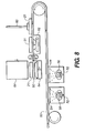
- the base 22 of the OLED light source 10 is adapted to be received by a socket 40 for connecting the OLED light source 10 to an external power source (such as a household electrical grid, not shown).
- Contacts 44 are provided in an aperture 42 in the socket 40 for contacting the conductors on the base 22 to supply power to the electrodes of the OLED.
- the base 22 and the aperture 42 may include complementary features such as a step to ensure that the base can be inserted in only one orientation into the socket aperture 42 so the base of the light source 10 cannot be inserted backwards into the socket.
- the light source 10 may be physically inserted into or removed from the socket by pushing or pulling the light source into or out of the socket.
- the base 22 and the socket 40 are preferably provided with a detent (not shown) to hold the light source 10 in the socket
- Duplicate first electrical contacts 44' may be replicated in the aperture 42 so that the base 22 (assuming it does not include an orientation feature) may be inserted in either orientation into the aperture 42 and will still connect appropriately to the power source.
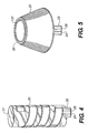
- the rigid support 21 may be curved to provide a three dimensional light emitting surface such as a cylinder (as shown in Fig. 3), a spiral (as shown in Fig. 4), or a conical surface (as shown in Fig. 5).
- the base 22 can be in the form of a conventional base such as a standard US light bulb base (as shown Fig. 3), or a standard European base.
- the rigid support may be either a curved sheet, or a solid having a curved surface.
- the curved surface may mimic the surfaces of conventional light bulbs or take the shape of a cylinder, spiral, or pyramid.
- the flexible substrate is not necessarily rectangular when flat, and may have a complex shape to match the shape of the surface of the rigid support to which it is attached.
- the light source 10 defines two bases 22 and 22' located at opposite edges of the rigid support 21 .
- One of the conductors 24 and 26 can be provided on each of the bases. Alternatively, both conductors can be provided on each base.
- the rigid support 21 may be a frame.
- the frame 21 holds the flexible substrate 20 in a desired configuration, such as a plane (as shown), or a cylinder.
- Base 22 is attached to the frame 21 and is electrically connected to the electrodes on the flexible substrate 20 .
- the frame may be reflective or transparent to maximize the light output from the light source 10 .
- the light source shown in Fig. 7 may be manufactured by first forming the OLED layer, electrode layers and encapsulating cover on the flexible substrate, and injection molding the frame around the periphery of the flexible substrate.
- the base includes conductors that are in electrical contact with the electrodes and be molded together with the frame.
- the electrodes and OLED layer may be formed on the flexible substrate in a continuous process by providing a web of substrate material 50 in a roll that is sequentially advanced through a series of stations, including a plurality of material deposition stations 52 .
- the deposition stations may include electrode deposition stations where a conductive materials 56 are applied, for example by sputtering through a mask 54 onto the substrate; OLED material deposition stations where OLED materials 58 are applied to the substrate, and other stations for applying other layers such as electrode protection layers, electrical connections and an encapsulating cover layer.
- the rigid support 21 is subsequently attached to the flexible substrate at a station 60 .
- the rigid support may be provided with conductors and adhesives prior to attachment to the flexible substrate for example using printed circuit board techniques.
- the adhesives are then cured at a station 62 and the completed light source is cut from the continuous web at a die cutting station 64 .
- light source 10 may include a power converter 45 for converting the electrical power from the external power source to a form suitable for powering the OLED light source 10 .
- the external power source is a standard power source, for example, the power supplied to a house or office at 110 V in the United States or 220 V in the United Kingdom. Other standards such as 24 V DC, 12 V DC and 6 V DC found in vehicles, for example, may also be used.
- the OLED light source 10 may require a rectified voltage with a particular waveform and magnitude; the converter 45 can provide the particular waveform using conventional power control circuitry.
- the particular waveform may periodically reverse bias the light emitting organic materials to prolong the life-time of the OLED materials.
- the converter 45 may be integrated into the base 22 .
- the flexible substrates 20 may be standardized and may be used with a variety of bases and converters for different national markets to provide advantages of manufacturing and marketing scale.
- the substrate 20 and/or encapsulating cover may be suitably treated to provide directional lighting.
- the cover, substrate, or one of the electrodes may be provided with a reflective surface so that light emitted by the OLED layer will travel through the other surface and the device will emit light on only one side.
- the external surface of the substrate or cover may be treated or modified to improve light output characteristics, for example by frosting to provide light diffusion.
- a transparent or translucent screen or housing 70 may be provided around the OLED light source 10 to diffuse the light and provide additional physical protection and aesthetic appeal.
- the housing may take a variety of shapes, for example the shape of a standard light bulb as shown.
- the present invention may be employed in a wide variety of conventional applications, for example in a table-top lamp, floor-lamp, chandelier, under-counter lamp, or ceiling light.
- the present invention may also be employed in portable illumination devices using DC power sources.
- the Organic Light Emitting Diode (OLED) layer is composed of small molecule OLED material as disclosed in but not limited to US Patent 4,769,292, issued September 6, 1988 to Tang et al., and US Patent 5,061,569, issued October 29, 1991 to VanSlyke et al.
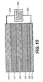
- a typical, non-limiting structure is shown in Figure 10 and is comprised of an anode layer 103 , a hole-injecting layer 105 , a hole-transporting layer 107 , a light-emitting layer 109 , an electron-transporting layer 111 , and a cathode layer 113 . These layers are described in detail below.
- the total combined thickness of the organic layers is preferably less than 500 nm.
- a voltage/current source 250 is required to energize the OLED element and conductive wiring 260 is required to make electrical contact to the anode and cathode.
- the TFT layers and associated wiring serve these functions.
- Substrate 20 is preferably light transmissive but may also be opaque.
- Substrates for use in this case include, but are not limited to, glass, plastic, semiconductor materials, ceramics, and circuit board materials.
- the anode layer 103 is preferably transparent or substantially transparent to the light emitted by the OLED layer(s).
- Common transparent anode materials used in this invention are indium-tin oxide (ITO), indium-zinc oxide (IZO) and tin oxide, but other metal oxides can work including, but not limited to, aluminum- or indium-doped zinc oxide, magnesium-indium oxide, and nickel-tungsten oxide.
- metal nitrides such as gallium nitride
- metal selenides such as zinc selenide
- metal sulfides such as zinc sulfide
- the light transmitting characteristics of layer 103 are immaterial and any conductive material can be used, transparent, opaque or reflective.
- Example conductors for this application include, but are not limited to, gold, iridium, molybdenum, palladium, and platinum.
- Typical anode materials, transmissive or otherwise, have a work function of 4.1 eV or greater. Desired anode materials are commonly deposited by any suitable means such as evaporation, sputtering, chemical vapor deposition, or electrochemical means.
- Anodes can be patterned using well-known photolithographic processes.
- a hole-injecting layer 105 be provided between anode 103 and hole-transporting layer 107 .
- the hole-injecting material can serve to improve the film formation property of subsequent organic layers and to facilitate injection of holes into the hole-transporting layer.
- Suitable materials for use in the hole-injecting layer include, but are not limited to, porphyrinic compounds as described in US 4,720,432, and plasma-deposited fluorocarbon polymers as described in US 6,208,075.
- Alternative hole-injecting materials reportedly useful in organic EL devices are described in EP 0 891 121 A1 and EP 1 029 909 A1.
- the hole-transporting layer 107 contains at least one hole-transporting compound such as an aromatic tertiary amine, where the latter is understood to be a compound containing at least one trivalent nitrogen atom that is bonded only to carbon atoms, at least one of which is a member of an aromatic ring.
- the aromatic tertiary amine can be an arylamine, such as a monoarylamine, diarylamine, triarylamine, or a polymeric arylamine. Exemplary monomeric triarylamines are illustrated by Klupfel et al. US 3,180,730.
- aromatic tertiary amines substituted with one or more vinyl radicals and/or comprising at least one active hydrogen containing group are disclosed by Brantley et al US 3,567,450 and US 3,658,520.
- a more preferred class of aromatic tertiary amines are those which include at least two aromatic tertiary amine moieties as described in US 4,720,432 and US 5,061,569.
- Illustrative of useful aromatic tertiary amines include, but are not limited to, the following:
- Another class of useful hole-transporting materials includes polycyclic aromatic compounds as described in EP 1 009 041.
- polymeric hole-transporting materials can be used such as poly(N-vinylcarbazole) (PVK), polythiophenes, polypyrrole, polyaniline, and copolymers such as poly(3,4-ethylenedioxythiophene) / poly(4-styrenesulfonate) also called PEDOT/PSS.
- the light-emitting layer (LEL) 109 of the organic EL element comprises a luminescent or fluorescent material where electroluminescence is produced as a result of electron-hole pair recombination in this region.
- the light-emitting layer can be comprised of a single material, but more commonly consists of a host material doped with a guest compound or compounds where light emission comes primarily from the dopant and can be of any color.
- the host materials in the light-emitting layer can be an electron-transporting material, as defined below, a hole-transporting material, as defined above, or another material or combination of materials that support hole-electron recombination.
- the dopant is usually chosen from highly fluorescent dyes, but phosphorescent compounds, e.g., transition metal complexes as described in WO 98/55561, WO 00/18851, WO 00/57676, and WO 00/70655 are also useful. Dopants are typically coated as 0.01 to 10 % by weight into the host material. Iridium complexes of phenylpyridine and its derivatives are particularly useful luminescent dopants. Polymeric materials such as polyfluorenes and polyvinylarylenes (e.g., poly(p-phenylenevinylene), PPV) can also be used as the host material. In this case, small molecule dopants can be molecularly dispersed into the polymeric host, or the dopant could be added by copolymerizing a minor constituent into the host polymer.
- phosphorescent compounds e.g., transition metal complexes as described in WO 98/55561, WO 00/18851, WO 00
- Host and emitting molecules known to be of use include, but are not limited to, those disclosed in US 4,769,292, US 5,141,671, US 5,150,006, US 5,151,629, US 5,405,709, US 5,484,922, US 5,593,788, US 5,645,948, US 5,683,823, US 5,755,999, US 5,928,802, US 5,935,720, US 5,935,721, and US 6,020,078.
- Metal complexes of 8-hydroxyquinoline and similar oxine derivatives constitute one class of useful host compounds capable of supporting electroluminescence, and are particularly suitable.
- useful chelated oxinoid compounds are the following:
- useful host materials include, but are not limited to: derivatives of anthracene, such as 9,10-di-(2-naphthyl)anthracene and derivatives thereof, distyrylarylene derivatives as described in US 5,121,029, and benzazole derivatives, for example, 2, 2', 2"-(1,3,5-phenylene)tris[1-phenyl-1H-benzimidazole].
- Useful fluorescent dopants include, but are not limited to, derivatives of anthracene, tetracene, xanthene, perylene, rubrene, coumarin, rhodamine, quinacridone, dicyanomethylenepyran compounds, thiopyran compounds, polymethine compounds, pyrilium and thiapyrilium compounds, fluorene derivatives, periflanthene derivatives and carbostyryl compounds.
- Preferred thin film-forming materials for use in forming the electron-transporting layer 111 of the organic EL elements of this invention are metal chelated oxinoid compounds, including chelates of oxine itself (also commonly referred to as 8-quinolinol or 8-hydroxyquinoline). Such compounds help to inject and transport electrons, exhibit high levels of performance, and are readily fabricated in the form of thin films. Exemplary oxinoid compounds were listed previously.
- electron-transporting materials include various butadiene derivatives as disclosed in US 4,356,429 and various heterocyclic optical brighteners as described in US 4,539,507. Benzazoles and triazines are also useful electron-transporting materials.
- layers 111 and 109 can optionally be collapsed into a single layer that serves the function of supporting both light emission and electron transport. These layers can be collapsed in both small molecule OLED systems and in polymeric OLED systems.
- a hole-transporting layer such as PEDOT-PSS with a polymeric light-emitting layer such as PPV.
- PPV serves the function of supporting both light emission and electron transport.
- the cathode 113 is transparent and can comprise nearly any conductive transparent material.
- the cathode 113 may be opaque or reflective.
- Suitable cathode materials have good film-forming properties to ensure good contact with the underlying organic layer, promote electron injection at low voltage, and have good stability.
- Useful cathode materials often contain a low work function metal ( ⁇ 4.0 eV) or metal alloy.
- One preferred cathode material is comprised of a Mg:Ag alloy wherein the percentage of silver is in the range of 1 to 20 %, as described in US Patent 4,885,221.
- Another suitable class of cathode materials includes bilayers comprising a thin electron-injection layer (EIL) and a thicker layer of conductive metal.
- the EIL is situated between the cathode and the organic layer (e.g., ETL).
- the EIL preferably includes a low work function metal or metal salt, and if so, the thicker conductor layer does not need to have a low work function.
- One such cathode is comprised of a thin layer of LiF followed by a thicker layer of A1 as described in US 5,677,572.
- Other useful cathode material sets include, but are not limited to, those disclosed in US 5,059,861, 5,059,862, and 6,140,763.
- cathode layer 113 When cathode layer 113 is transparent or nearly transparent, metals must be thin or transparent conductive oxides, or a combination of these materials.
- Optically transparent cathodes have been described in more detail in US 4,885,211, US 5,247,190, JP 3,234,963, US 5,703,436, US 5,608,287, US 5,837,391, US 5,677,572, US 5,776,622, US 5,776,623, US 5,714,838, US 5,969,474, US 5,739,545, US 5,981,306, US 6,137,223, US 6,140,763, US 6,172,459, EP 1 076 368, and US 6,278,236.
- Cathode materials are typically deposited by evaporation, sputtering, or chemical vapor deposition. When needed, patterning can be achieved through many well known methods including, but not limited to, through-mask deposition, integral shadow masking as described in US 5,276,380 and EP 0 732 868, laser ablation, and selective chemical vapor deposition.
- the organic materials mentioned above are suitably deposited through a vapor-phase method such as sublimation, but can be deposited from a fluid, for example, from a solvent with an optional binder to improve film formation. If the material is a polymer, solvent deposition is useful but other methods can be used, such as sputtering or thermal transfer from a donor sheet.
- the material to be deposited by sublimation can be vaporized from a sublimator "boat" often comprised of a tantalum material, e.g., as described in US 6,237,529, or can be first coated onto a donor sheet and then sublimed in closer proximity to the substrate.
- Layers with a mixture of materials can utilize separate sublimator boats or the materials can be pre-mixed and coated from a single boat or donor sheet. Patterned deposition can be achieved using shadow masks, integral shadow masks (US 5,294,870), spatially-defined thermal dye transfer from a donor sheet (US 5,851,709 and 6,066,357) and inkjet method (US 6,066,357). While all organic layers may be patterned, it is most common that only the layer emitting light is patterned, and the other layers may be uniformly deposited over the entire device.
- OLED devices of this invention can employ various well-known optical effects in order to enhance its properties if desired. This includes optimizing layer thicknesses to yield maximum light transmission, providing dielectric mirror structures, replacing reflective electrodes with light-absorbing electrodes, providing anti-glare or anti-reflection coatings over the device, providing a polarizing medium over the device, or providing colored, neutral density, or color conversion filters over the device. Filters, polarizers, and anti-glare or anti-reflection coatings may be specifically provided over the cover or as part of the cover.
Landscapes
- Engineering & Computer Science (AREA)
- Physics & Mathematics (AREA)
- Microelectronics & Electronic Packaging (AREA)
- Optics & Photonics (AREA)
- General Engineering & Computer Science (AREA)
- Electroluminescent Light Sources (AREA)
- Fastening Of Light Sources Or Lamp Holders (AREA)
- Non-Portable Lighting Devices Or Systems Thereof (AREA)
- Planar Illumination Modules (AREA)
Applications Claiming Priority (2)
| Application Number | Priority Date | Filing Date | Title |
|---|---|---|---|
| US10/156,494 US6787990B2 (en) | 2002-05-28 | 2002-05-28 | OLED area illumination light source having flexible substrate on a support |
| US156494 | 2002-05-28 |
Publications (2)
| Publication Number | Publication Date |
|---|---|
| EP1367676A1 true EP1367676A1 (de) | 2003-12-03 |
| EP1367676B1 EP1367676B1 (de) | 2006-07-12 |
Family
ID=29419625
Family Applications (1)
| Application Number | Title | Priority Date | Filing Date |
|---|---|---|---|
| EP20030076478 Expired - Lifetime EP1367676B1 (de) | 2002-05-28 | 2003-05-16 | Vorrichtung mit organischen lichtemittierenden Dioden mit einem flexiblen Substrat auf einem Träger |
Country Status (6)
| Country | Link |
|---|---|
| US (1) | US6787990B2 (de) |
| EP (1) | EP1367676B1 (de) |
| JP (1) | JP2004006366A (de) |
| KR (1) | KR20030091826A (de) |
| DE (1) | DE60306722T2 (de) |
| TW (1) | TWI280071B (de) |
Cited By (17)
| Publication number | Priority date | Publication date | Assignee | Title |
|---|---|---|---|---|
| WO2005099310A2 (en) | 2004-03-29 | 2005-10-20 | Articulated Technologies, Llc | Roll-to-roll fabricated light sheet and encapsulated semiconductor circuit devices |
| WO2009074322A1 (de) * | 2007-12-13 | 2009-06-18 | Thomas Emde | Leuchtmittel |
| WO2009118678A1 (en) * | 2008-03-26 | 2009-10-01 | Philips Intellectual Property & Standards Gmbh | Light emitting diode device |
| EP2138752A1 (de) * | 2008-06-27 | 2009-12-30 | Yamagata Promotional Organization for Industrial Technology | Beleuchtungsvorrichtung |
| CN102065593A (zh) * | 2009-10-27 | 2011-05-18 | 松下电工株式会社 | 发光模块 |
| CN102227584A (zh) * | 2008-11-26 | 2011-10-26 | 德洛伦·E·安德森 | 发光二极管模块 |
| DE102011002480A1 (de) * | 2011-01-05 | 2012-07-05 | Trilux Gmbh & Co. Kg | Leuchte mit flexibler OLED und Rahmen |
| WO2012148382A1 (en) * | 2011-04-26 | 2012-11-01 | The Procter & Gamble Company | Light bulb with loop illumination element |
| WO2012148384A1 (en) * | 2011-04-26 | 2012-11-01 | The Procter & Gamble Company | Stemmed lighting assembly with disk-shaped illumination element |
| WO2013025263A1 (en) * | 2011-04-13 | 2013-02-21 | General Electric Company | Fixture and socket assembly for replaceable and flexible panel lighting device |
| EP2639495A2 (de) * | 2012-03-16 | 2013-09-18 | Paul E. Lohneis | Dreidimensionale Beleuchtungsstruktur mit lichtaktiver Technologie |
| US8845117B2 (en) | 2008-04-15 | 2014-09-30 | Paul E. Lohneis | Three-dimensional lighting structure utilizing light active technology |
| US8979290B2 (en) | 2008-04-15 | 2015-03-17 | Paul E. Lohneis | Three-dimensional lighting structure utilizing light active technology |
| CN105531533A (zh) * | 2013-09-09 | 2016-04-27 | 法雷奥照明公司 | 包括有机发光二极管的灯模块 |
| EP2375862A3 (de) * | 2010-04-07 | 2017-11-29 | Panasonic Intellectual Property Management Co., Ltd. | Organisches EL-Modul und Beleuchtungsvorrichtung |
| EP3309854A1 (de) * | 2016-10-17 | 2018-04-18 | odelo GmbH | Oled umfassendes leuchtmittel für fahrzeugleuchte |
| CN105531533B (zh) * | 2013-09-09 | 2018-08-31 | 法雷奥照明公司 | 包括有机发光二极管的灯模块 |
Families Citing this family (82)
| Publication number | Priority date | Publication date | Assignee | Title |
|---|---|---|---|---|
| US7286271B2 (en) * | 2002-05-13 | 2007-10-23 | Transpacific Ip, Ltd. | Scanning chassis with a light transparent slot |
| US7364315B2 (en) * | 2002-06-14 | 2008-04-29 | Tseng-Lu Chien | Tubular electro-luminescent panel(s) light device |
| US6965197B2 (en) * | 2002-10-01 | 2005-11-15 | Eastman Kodak Company | Organic light-emitting device having enhanced light extraction efficiency |
| JP2004294163A (ja) * | 2003-03-26 | 2004-10-21 | Yazaki Corp | 車両計器用文字板、文字板製造方法、及び、文字板製造装置 |
| US20040232434A1 (en) * | 2003-05-21 | 2004-11-25 | Yen Tseng Technology Corporation | Electroluminescent lamp |
| US7432124B2 (en) * | 2003-11-04 | 2008-10-07 | 3M Innovative Properties Company | Method of making an organic light emitting device |
| US7271534B2 (en) * | 2003-11-04 | 2007-09-18 | 3M Innovative Properties Company | Segmented organic light emitting device |
| KR20050104065A (ko) * | 2004-04-28 | 2005-11-02 | (주)케이디티 | 가요성 평면 유기 발광 원 |
| US7108392B2 (en) * | 2004-05-04 | 2006-09-19 | Eastman Kodak Company | Tiled flat panel lighting system |
| WO2005122646A1 (ja) * | 2004-06-14 | 2005-12-22 | National Institute Of Advanced Industrial Scienceand Technology | 線状発光体、線状発光装置及び線状発光体の製造方法 |
| US7750352B2 (en) * | 2004-08-10 | 2010-07-06 | Pinion Technologies, Inc. | Light strips for lighting and backlighting applications |
| US9874332B1 (en) * | 2013-01-15 | 2018-01-23 | Steven Michael Colby | Bulb including removable cover |
| US11320129B1 (en) | 2004-10-05 | 2022-05-03 | Steven Michael Colby | LED bulb including pulse generator and/or AC/DC converter |
| US20060175967A1 (en) * | 2005-02-07 | 2006-08-10 | Miller Engineering Llc | Animated miniature electroluminescent billboards with hidden conductors |
| KR100698911B1 (ko) * | 2005-03-25 | 2007-03-26 | 이창남 | 말뚝 뺀 구멍을 채우는 연약지반 수평다짐공법 |
| JP4618002B2 (ja) * | 2005-05-26 | 2011-01-26 | パナソニック電工株式会社 | 照明装置 |
| US7575332B2 (en) * | 2005-06-21 | 2009-08-18 | Eastman Kodak Company | Removable flat-panel lamp and fixture |
| KR100674212B1 (ko) * | 2005-11-30 | 2007-01-24 | 주식회사 나모텍 | 소켓타입의 유기발광소자로 구성된 디스플레이장치 및 그제작방법 |
| JP2007165811A (ja) | 2005-12-16 | 2007-06-28 | Nichia Chem Ind Ltd | 発光装置 |
| US20070144045A1 (en) * | 2005-12-23 | 2007-06-28 | Lexmark International, Inc. | Electroluminescent display system |
| US7629742B2 (en) * | 2006-03-17 | 2009-12-08 | Lexmark International, Inc. | Electroluminescent displays, media, and members, and methods associated therewith |
| DE102006015437A1 (de) * | 2006-03-31 | 2007-10-04 | Merck Patent Gmbh | Leuchtfliese |
| JP5363985B2 (ja) * | 2006-10-19 | 2013-12-11 | コーニンクレッカ フィリップス エヌ ヴェ | 植物発育装置 |
| US8092034B2 (en) * | 2007-11-07 | 2012-01-10 | Richard David Ashoff | Illuminated tile systems and methods for manufacturing the same |
| DE202007019488U1 (de) | 2007-12-13 | 2012-12-10 | Emdeoled Gmbh | Leuchtmittel |
| DE202007019492U1 (de) | 2007-12-13 | 2013-01-11 | Emdeoled Gmbh | Leuchtmittel |
| JP5020113B2 (ja) * | 2008-02-07 | 2012-09-05 | 富士フイルム株式会社 | エレクトロルミネッセンス発光装置並びにそれを構成する発光板及び支持体 |
| JP2009211828A (ja) * | 2008-02-29 | 2009-09-17 | Rohm Co Ltd | 照明装置及び照明装置の製造方法 |
| JP5050977B2 (ja) * | 2008-04-16 | 2012-10-17 | パナソニック株式会社 | 面状発光型照明器具、および照明システム |
| DE102008031533B4 (de) * | 2008-07-03 | 2021-10-21 | Pictiva Displays International Limited | Organisches elektronisches Bauelement |
| US8214084B2 (en) | 2008-10-24 | 2012-07-03 | Ilumisys, Inc. | Integration of LED lighting with building controls |
| US8653984B2 (en) | 2008-10-24 | 2014-02-18 | Ilumisys, Inc. | Integration of LED lighting control with emergency notification systems |
| US7938562B2 (en) | 2008-10-24 | 2011-05-10 | Altair Engineering, Inc. | Lighting including integral communication apparatus |
| US8901823B2 (en) | 2008-10-24 | 2014-12-02 | Ilumisys, Inc. | Light and light sensor |
| US20100104780A1 (en) * | 2008-10-27 | 2010-04-29 | Paxton Donald J | Printed el foil for backlit airbag emblem |
| US8061861B2 (en) * | 2008-10-27 | 2011-11-22 | Autoliv Asp, Inc. | Method for illuminating colors in a backlit driver airbag emblem |
| US8251543B2 (en) | 2008-11-22 | 2012-08-28 | Innovative Lighting, Inc. | Interior corner mounting module for rope light system |
| US20100194080A1 (en) * | 2009-01-30 | 2010-08-05 | Paxton Donald J | Methods for illumination of driver airbag emblems |
| US8405116B2 (en) | 2009-03-18 | 2013-03-26 | Semiconductor Energy Laboratory Co., Ltd. | Lighting device |
| US8847480B2 (en) * | 2009-03-18 | 2014-09-30 | Semiconductor Energy Laboratory Co., Ltd. | Lighting device |
| WO2010106897A1 (en) * | 2009-03-18 | 2010-09-23 | Semiconductor Energy Laboratory Co., Ltd. | Lighting device |
| US20100247747A1 (en) * | 2009-03-27 | 2010-09-30 | Semiconductor Energy Laboratory Co., Ltd. | Film Deposition Apparatus, Method for Depositing Film, and Method for Manufacturing Lighting Device |
| US20120112618A1 (en) * | 2009-07-29 | 2012-05-10 | Sharp Kabushiki Kaisha | Organic electroluminescence illuminating device and method for manufacturing the same |
| US8172427B2 (en) * | 2009-11-25 | 2012-05-08 | Fu-Hsien Hsu | LED decorative lamp |
| EP2553332B1 (de) * | 2010-03-26 | 2016-03-23 | iLumisys, Inc. | Umgestülpte led-glühlampe |
| CN103109389B (zh) | 2010-09-27 | 2016-01-20 | 皇家飞利浦电子股份有限公司 | 具有柔性覆盖层的oled |
| DE102010038251A1 (de) * | 2010-10-18 | 2012-04-19 | Koninklijke Philips Electronics N.V. | OLED-Leuchtmittel für eine Leuchte |
| DE102010038252A1 (de) * | 2010-10-18 | 2012-04-19 | Koninklijke Philips Electronics N.V. | Fassung für eine Leuchte mit OLED-Leuchtmittel |
| KR101889857B1 (ko) | 2011-01-24 | 2018-08-20 | 가부시키가이샤 한도오따이 에네루기 켄큐쇼 | 조명장치 및 조명장치의 설치보드 |
| US8314566B2 (en) | 2011-02-22 | 2012-11-20 | Quarkstar Llc | Solid state lamp using light emitting strips |
| US8410726B2 (en) * | 2011-02-22 | 2013-04-02 | Quarkstar Llc | Solid state lamp using modular light emitting elements |
| US20140049972A1 (en) * | 2011-04-26 | 2014-02-20 | The Procter & Gamble Company | Stemmed lighting assembly with disk-shaped illumination element |
| US8710518B2 (en) | 2011-05-12 | 2014-04-29 | Universal Display Corporation | Flexible lighting devices |
| US8773013B2 (en) | 2011-05-12 | 2014-07-08 | Universal Display Corporation | Three dimensional OLED lamps |
| US9109764B2 (en) * | 2011-10-12 | 2015-08-18 | Ip Design Llc | Durable lighting apparatus with isotropic radiation pattern |
| US9271367B2 (en) | 2012-07-09 | 2016-02-23 | Ilumisys, Inc. | System and method for controlling operation of an LED-based light |
| EP2986901B1 (de) * | 2013-03-06 | 2018-06-13 | Cooper Technologies Company | Leuchten mit flexiblem substrat |
| JP5584792B2 (ja) * | 2013-03-26 | 2014-09-03 | パナソニック株式会社 | 光源装置 |
| RU2015145491A (ru) | 2013-03-27 | 2017-05-16 | ОЛЕДВоркс ГмбХ | МОДЕРНИЗИРОВАННЫЙ ИСТОЧНИК СВЕТА НА ОРГАНИЧЕСКИХ СВЕТОИЗЛУЧАЮЩИХ ДИОДАХ (ОСИДах) |
| US9041297B2 (en) | 2013-05-20 | 2015-05-26 | Universal Display Corporation | Large area lighting system with wireless control |
| US9482393B2 (en) | 2013-06-07 | 2016-11-01 | John E. Shirilla | Flexible light panel for professional use |
| US10033141B2 (en) | 2013-10-04 | 2018-07-24 | Philips Lighting Holding B.V. | Lighting device connector comprising a heat sink |
| JP6400285B2 (ja) * | 2013-10-23 | 2018-10-03 | パイオニア株式会社 | 発光装置 |
| DE102013020782A1 (de) * | 2013-12-13 | 2015-06-18 | GM Global Technology Operations, LLC (n.d. Ges. d. Staates Delaware) | Fahrzeug mit Leuchtanzeigeinstrument |
| WO2015112437A1 (en) | 2014-01-22 | 2015-07-30 | Ilumisys, Inc. | Led-based light with addressed leds |
| US9651230B1 (en) | 2014-02-07 | 2017-05-16 | Sourcemaker, Inc. | Flexible lighting apparatus |
| US9281298B2 (en) | 2014-02-10 | 2016-03-08 | Nthdegree Technologies Worldwide Inc. | Process for forming ultra-micro LEDS |
| CA2843101A1 (en) * | 2014-02-20 | 2015-08-20 | Matthew Kennedy | Flexible oled panel fashioned to resemble a lamp shade |
| CA2843575A1 (en) * | 2014-02-25 | 2015-08-25 | Matthew Kennedy | Led lighting fixture with a light emitting waveguide resembling a lamp shade |
| US9510400B2 (en) | 2014-05-13 | 2016-11-29 | Ilumisys, Inc. | User input systems for an LED-based light |
| KR101955905B1 (ko) * | 2014-07-18 | 2019-03-08 | 엘지디스플레이 주식회사 | 조명 장치 |
| US10161568B2 (en) | 2015-06-01 | 2018-12-25 | Ilumisys, Inc. | LED-based light with canted outer walls |
| US10918747B2 (en) | 2015-07-30 | 2021-02-16 | Vital Vio, Inc. | Disinfecting lighting device |
| KR102288354B1 (ko) * | 2015-08-10 | 2021-08-11 | 삼성디스플레이 주식회사 | 플렉서블 디스플레이 장치의 제조 방법 |
| US9803852B1 (en) * | 2015-12-08 | 2017-10-31 | Kevin Clacken | Illuminated headset |
| JP6632738B2 (ja) * | 2016-02-26 | 2020-01-22 | オーレッドワークス エルエルシー | 平坦な照明モジュールのための着脱可能な電気接続部 |
| DE202016103453U1 (de) | 2016-06-29 | 2017-10-06 | Emdedesign Gmbh | Leuchte umfassend ein flexibles OLED-Leuchtmittel |
| DE102017116151A1 (de) * | 2017-07-18 | 2019-01-24 | Ledvance Gmbh | Leuchtmittel mit selbstleuchtender Schicht |
| US10617774B2 (en) * | 2017-12-01 | 2020-04-14 | Vital Vio, Inc. | Cover with disinfecting illuminated surface |
| US11506363B2 (en) | 2018-01-09 | 2022-11-22 | OLEDWorks LLC | Ultrathin OLED lighting panel |
| WO2021030748A1 (en) | 2019-08-15 | 2021-02-18 | Vital Vio, Inc. | Devices configured to disinfect interiors |
| US11878084B2 (en) | 2019-09-20 | 2024-01-23 | Vyv, Inc. | Disinfecting light emitting subcomponent |
Citations (4)
| Publication number | Priority date | Publication date | Assignee | Title |
|---|---|---|---|---|
| US5667394A (en) * | 1995-02-03 | 1997-09-16 | Chien; Tseng Lu | Electro-luminescent strip and connector set therefor |
| WO1999057945A1 (en) * | 1998-05-04 | 1999-11-11 | Fiber Optic Designs, Inc. | A lamp employing a monolithic led device |
| EP1120838A2 (de) * | 2000-01-27 | 2001-08-01 | General Electric Company | Organisches lichtemittierendes Bauelement und Montageverfahren |
| US6274978B1 (en) * | 1999-02-23 | 2001-08-14 | Sarnoff Corporation | Fiber-based flat panel display |
Family Cites Families (23)
| Publication number | Priority date | Publication date | Assignee | Title |
|---|---|---|---|---|
| US4211955A (en) * | 1978-03-02 | 1980-07-08 | Ray Stephen W | Solid state lamp |
| US4138620A (en) * | 1978-03-24 | 1979-02-06 | Minnesota Mining And Manufacturing Company | Multi-panel electroluminescent light assembly |
| US4745334A (en) * | 1985-10-25 | 1988-05-17 | Alps Electric Co., Ltd. | Electroluminescent element and method for connecting its terminals |
| US4769292A (en) | 1987-03-02 | 1988-09-06 | Eastman Kodak Company | Electroluminescent device with modified thin film luminescent zone |
| JPH0727598Y2 (ja) * | 1988-10-17 | 1995-06-21 | アルプス電気株式会社 | エレクトロルミネセンス |
| JPH02259726A (ja) * | 1989-03-31 | 1990-10-22 | Toshiba Corp | 透明導電性フィルム、分散型elパネルおよび液晶表示装置 |
| US5266865A (en) * | 1989-08-22 | 1993-11-30 | Nec Corporation | Structure of lead conductor for third electrode of three-electrode type electroluminescent lamp |
| US5061569A (en) | 1990-07-26 | 1991-10-29 | Eastman Kodak Company | Electroluminescent device with organic electroluminescent medium |
| US6124672A (en) * | 1995-03-30 | 2000-09-26 | Dynamic Brilliance Corporation | Electroluminescent device with a secure contact |
| EP0996313A3 (de) * | 1995-07-14 | 2000-08-02 | Matsushita Electric Industrial Co., Ltd. | Beleuchteter Schalter |
| JPH0935571A (ja) * | 1995-07-14 | 1997-02-07 | Matsushita Electric Ind Co Ltd | 照光式スイッチユニット |
| JPH09102392A (ja) * | 1995-10-06 | 1997-04-15 | Idemitsu Kosan Co Ltd | 有機elパネルおよびこのパネルを用いた表示装置 |
| TW337055B (en) * | 1996-03-29 | 1998-07-21 | Toshiba Co Ltd | EL screen packing film and the manufacturing method, the EL screen and the LCD module |
| GB2335884A (en) | 1998-04-02 | 1999-10-06 | Cambridge Display Tech Ltd | Flexible substrates for electronic or optoelectronic devices |
| US6036336A (en) * | 1998-05-08 | 2000-03-14 | Wu; Chen H. | Light emitting diode retrofitting lamps for illuminated traffic signs |
| US6218785B1 (en) * | 1999-03-19 | 2001-04-17 | Incerti & Simonini Di Incerti Edda & C. S.N.C. | Low-tension lighting device |
| JP2001015264A (ja) * | 1999-06-29 | 2001-01-19 | Minolta Co Ltd | 平面発光体 |
| US6579422B1 (en) * | 1999-07-07 | 2003-06-17 | Sony Corporation | Method and apparatus for manufacturing flexible organic EL display |
| JP4246333B2 (ja) * | 1999-10-29 | 2009-04-02 | 富士重工業株式会社 | 車両用ランプ |
| JP2001325805A (ja) * | 2000-05-15 | 2001-11-22 | Matsushita Electric Works Ltd | スタンド形照明器具 |
| US6515314B1 (en) * | 2000-11-16 | 2003-02-04 | General Electric Company | Light-emitting device with organic layer doped with photoluminescent material |
| TW486072U (en) * | 2000-12-06 | 2002-05-01 | Ritek Corp | Night light with luminous disk |
| US6565231B1 (en) * | 2002-05-28 | 2003-05-20 | Eastman Kodak Company | OLED area illumination lighting apparatus |
-
2002
- 2002-05-28 US US10/156,494 patent/US6787990B2/en not_active Expired - Lifetime
-
2003
- 2003-04-08 TW TW92107996A patent/TWI280071B/zh not_active IP Right Cessation
- 2003-05-16 DE DE2003606722 patent/DE60306722T2/de not_active Expired - Lifetime
- 2003-05-16 EP EP20030076478 patent/EP1367676B1/de not_active Expired - Lifetime
- 2003-05-27 KR KR10-2003-0033775A patent/KR20030091826A/ko not_active Application Discontinuation
- 2003-05-27 JP JP2003148935A patent/JP2004006366A/ja active Pending
Patent Citations (4)
| Publication number | Priority date | Publication date | Assignee | Title |
|---|---|---|---|---|
| US5667394A (en) * | 1995-02-03 | 1997-09-16 | Chien; Tseng Lu | Electro-luminescent strip and connector set therefor |
| WO1999057945A1 (en) * | 1998-05-04 | 1999-11-11 | Fiber Optic Designs, Inc. | A lamp employing a monolithic led device |
| US6274978B1 (en) * | 1999-02-23 | 2001-08-14 | Sarnoff Corporation | Fiber-based flat panel display |
| EP1120838A2 (de) * | 2000-01-27 | 2001-08-01 | General Electric Company | Organisches lichtemittierendes Bauelement und Montageverfahren |
Cited By (34)
| Publication number | Priority date | Publication date | Assignee | Title |
|---|---|---|---|---|
| WO2005099310A2 (en) | 2004-03-29 | 2005-10-20 | Articulated Technologies, Llc | Roll-to-roll fabricated light sheet and encapsulated semiconductor circuit devices |
| EP1736035A2 (de) * | 2004-03-29 | 2006-12-27 | Articulated Technologies, Llc | Von rolle zu rolle hergestelltes lichtblatt und verkapselte halbleiter-schaltungsbauelemente |
| EP1736035A4 (de) * | 2004-03-29 | 2009-01-07 | Articulated Technologies Llc | Von rolle zu rolle hergestelltes lichtblatt und verkapselte halbleiter-schaltungsbauelemente |
| US8330355B2 (en) | 2007-12-13 | 2012-12-11 | Emdeoled Gmbh | Illumination means |
| WO2009074322A1 (de) * | 2007-12-13 | 2009-06-18 | Thomas Emde | Leuchtmittel |
| US8581292B2 (en) | 2008-03-26 | 2013-11-12 | Koninklijke Philips N.V. | Light emitting diode device |
| WO2009118678A1 (en) * | 2008-03-26 | 2009-10-01 | Philips Intellectual Property & Standards Gmbh | Light emitting diode device |
| US8979290B2 (en) | 2008-04-15 | 2015-03-17 | Paul E. Lohneis | Three-dimensional lighting structure utilizing light active technology |
| US8845117B2 (en) | 2008-04-15 | 2014-09-30 | Paul E. Lohneis | Three-dimensional lighting structure utilizing light active technology |
| EP2138752A1 (de) * | 2008-06-27 | 2009-12-30 | Yamagata Promotional Organization for Industrial Technology | Beleuchtungsvorrichtung |
| CN102227584A (zh) * | 2008-11-26 | 2011-10-26 | 德洛伦·E·安德森 | 发光二极管模块 |
| US9470372B2 (en) | 2008-11-26 | 2016-10-18 | Deloren E. Anderson | High intensity replaceable light emitting diode module and array |
| US8545060B2 (en) | 2008-11-26 | 2013-10-01 | Deloren E. Anderson | High intensity replaceable light emitting diode module and array |
| US10925139B2 (en) | 2008-11-26 | 2021-02-16 | Yjb Led, Inc. | High intensity replaceable light emitting diode module and array |
| US11178744B2 (en) | 2008-11-26 | 2021-11-16 | Yjb Led, Inc. | High intensity replaceable light emitting diode module and array |
| CN102227584B (zh) * | 2008-11-26 | 2014-07-23 | 德洛伦·E·安德森 | 发光二极管模块 |
| US11924943B2 (en) | 2008-11-26 | 2024-03-05 | Yjb Led, Inc. | High intensity replaceable light emitting diode module and array |
| EP2317583A3 (de) * | 2009-10-27 | 2012-05-30 | Panasonic Corporation | Lichtemittierendes Modul |
| CN102065593A (zh) * | 2009-10-27 | 2011-05-18 | 松下电工株式会社 | 发光模块 |
| CN102065593B (zh) * | 2009-10-27 | 2013-09-04 | 松下电器产业株式会社 | 发光模块 |
| US8419201B2 (en) | 2009-10-27 | 2013-04-16 | Panasonic Corporation | Light emitting module |
| EP2375862A3 (de) * | 2010-04-07 | 2017-11-29 | Panasonic Intellectual Property Management Co., Ltd. | Organisches EL-Modul und Beleuchtungsvorrichtung |
| DE102011002480A1 (de) * | 2011-01-05 | 2012-07-05 | Trilux Gmbh & Co. Kg | Leuchte mit flexibler OLED und Rahmen |
| WO2013025263A1 (en) * | 2011-04-13 | 2013-02-21 | General Electric Company | Fixture and socket assembly for replaceable and flexible panel lighting device |
| US8624483B2 (en) | 2011-04-13 | 2014-01-07 | General Electric Company | Fixture and socket assembly for replaceable and flexible panel lighting device |
| WO2012148384A1 (en) * | 2011-04-26 | 2012-11-01 | The Procter & Gamble Company | Stemmed lighting assembly with disk-shaped illumination element |
| WO2012148382A1 (en) * | 2011-04-26 | 2012-11-01 | The Procter & Gamble Company | Light bulb with loop illumination element |
| EP2639783A2 (de) * | 2012-03-16 | 2013-09-18 | Paul E. Lohneis | Dreidimensionale Beleuchtungsstruktur mit lichtaktiver Technologie |
| EP2639783A3 (de) * | 2012-03-16 | 2014-05-07 | Paul E. Lohneis | Dreidimensionale Beleuchtungsstruktur mit lichtaktiver Technologie |
| EP2639495A3 (de) * | 2012-03-16 | 2014-05-07 | Paul E. Lohneis | Dreidimensionale Beleuchtungsstruktur mit lichtaktiver Technologie |
| EP2639495A2 (de) * | 2012-03-16 | 2013-09-18 | Paul E. Lohneis | Dreidimensionale Beleuchtungsstruktur mit lichtaktiver Technologie |
| CN105531533A (zh) * | 2013-09-09 | 2016-04-27 | 法雷奥照明公司 | 包括有机发光二极管的灯模块 |
| CN105531533B (zh) * | 2013-09-09 | 2018-08-31 | 法雷奥照明公司 | 包括有机发光二极管的灯模块 |
| EP3309854A1 (de) * | 2016-10-17 | 2018-04-18 | odelo GmbH | Oled umfassendes leuchtmittel für fahrzeugleuchte |
Also Published As
| Publication number | Publication date |
|---|---|
| TW200308180A (en) | 2003-12-16 |
| DE60306722D1 (de) | 2006-08-24 |
| DE60306722T2 (de) | 2007-08-02 |
| TWI280071B (en) | 2007-04-21 |
| EP1367676B1 (de) | 2006-07-12 |
| US20030222578A1 (en) | 2003-12-04 |
| JP2004006366A (ja) | 2004-01-08 |
| US6787990B2 (en) | 2004-09-07 |
| KR20030091826A (ko) | 2003-12-03 |
Similar Documents
| Publication | Publication Date | Title |
|---|---|---|
| EP1367676B1 (de) | Vorrichtung mit organischen lichtemittierenden Dioden mit einem flexiblen Substrat auf einem Träger | |
| EP1367675B1 (de) | Vorrichtung mit organischen lichtemittierenden Dioden | |
| EP1367674B1 (de) | Vorrichtung mit organischen lichtemittierenden Dioden | |
| US6771021B2 (en) | Lighting apparatus with flexible OLED area illumination light source and fixture | |
| US7034470B2 (en) | Serially connecting OLED devices for area illumination | |
| EP1403908B1 (de) | Organische elektrolumineszierende Lampe | |
| US6693296B1 (en) | OLED apparatus including a series of OLED devices | |
| US6870196B2 (en) | Series/parallel OLED light source | |
| US20090135582A1 (en) | Electro-luminescent area illumination device | |
| WO2005078817A2 (en) | Manufacture of flat panel light emitting devices |
Legal Events
| Date | Code | Title | Description |
|---|---|---|---|
| PUAI | Public reference made under article 153(3) epc to a published international application that has entered the european phase |
Free format text: ORIGINAL CODE: 0009012 |
|
| AK | Designated contracting states |
Kind code of ref document: A1 Designated state(s): AT BE BG CH CY CZ DE DK EE ES FI FR GB GR HU IE IT LI LU MC NL PT RO SE SI SK TR |
|
| AX | Request for extension of the european patent |
Extension state: AL LT LV MK |
|
| 17P | Request for examination filed |
Effective date: 20040521 |
|
| AKX | Designation fees paid |
Designated state(s): DE FR GB |
|
| 17Q | First examination report despatched |
Effective date: 20040913 |
|
| GRAP | Despatch of communication of intention to grant a patent |
Free format text: ORIGINAL CODE: EPIDOSNIGR1 |
|
| RTI1 | Title (correction) |
Free format text: OLED AREA ILLUMINATION LIGHT SOURCE HAVING FLEXIBLE SUBSTRATE ON A SUPPORT |
|
| GRAS | Grant fee paid |
Free format text: ORIGINAL CODE: EPIDOSNIGR3 |
|
| GRAA | (expected) grant |
Free format text: ORIGINAL CODE: 0009210 |
|
| AK | Designated contracting states |
Kind code of ref document: B1 Designated state(s): DE FR GB |
|
| REG | Reference to a national code |
Ref country code: GB Ref legal event code: FG4D |
|
| REF | Corresponds to: |
Ref document number: 60306722 Country of ref document: DE Date of ref document: 20060824 Kind code of ref document: P |
|
| ET | Fr: translation filed | ||
| PLBE | No opposition filed within time limit |
Free format text: ORIGINAL CODE: 0009261 |
|
| STAA | Information on the status of an ep patent application or granted ep patent |
Free format text: STATUS: NO OPPOSITION FILED WITHIN TIME LIMIT |
|
| 26N | No opposition filed |
Effective date: 20070413 |
|
| REG | Reference to a national code |
Ref country code: FR Ref legal event code: TP |
|
| REG | Reference to a national code |
Ref country code: GB Ref legal event code: 732E Free format text: REGISTERED BETWEEN 20110224 AND 20110302 |
|
| REG | Reference to a national code |
Ref country code: FR Ref legal event code: PLFP Year of fee payment: 14 |
|
| REG | Reference to a national code |
Ref country code: FR Ref legal event code: PLFP Year of fee payment: 15 |
|
| REG | Reference to a national code |
Ref country code: FR Ref legal event code: PLFP Year of fee payment: 16 |
|
| PGFP | Annual fee paid to national office [announced via postgrant information from national office to epo] |
Ref country code: GB Payment date: 20220519 Year of fee payment: 20 Ref country code: FR Payment date: 20220523 Year of fee payment: 20 Ref country code: DE Payment date: 20220519 Year of fee payment: 20 |
|
| REG | Reference to a national code |
Ref country code: DE Ref legal event code: R071 Ref document number: 60306722 Country of ref document: DE |
|
| REG | Reference to a national code |
Ref country code: GB Ref legal event code: PE20 Expiry date: 20230515 |
|
| PG25 | Lapsed in a contracting state [announced via postgrant information from national office to epo] |
Ref country code: GB Free format text: LAPSE BECAUSE OF EXPIRATION OF PROTECTION Effective date: 20230515 |