EP1363404A1 - Pulsweitenmoduliertes Sensorausgangssignal - Google Patents
Pulsweitenmoduliertes Sensorausgangssignal Download PDFInfo
- Publication number
- EP1363404A1 EP1363404A1 EP03010032A EP03010032A EP1363404A1 EP 1363404 A1 EP1363404 A1 EP 1363404A1 EP 03010032 A EP03010032 A EP 03010032A EP 03010032 A EP03010032 A EP 03010032A EP 1363404 A1 EP1363404 A1 EP 1363404A1
- Authority
- EP
- European Patent Office
- Prior art keywords
- signal
- inverted
- sensor output
- output signal
- signal according
- Prior art date
- Legal status (The legal status is an assumption and is not a legal conclusion. Google has not performed a legal analysis and makes no representation as to the accuracy of the status listed.)
- Granted
Links
Images
Classifications
-
- G—PHYSICS
- G11—INFORMATION STORAGE
- G11B—INFORMATION STORAGE BASED ON RELATIVE MOVEMENT BETWEEN RECORD CARRIER AND TRANSDUCER
- G11B20/00—Signal processing not specific to the method of recording or reproducing; Circuits therefor
- G11B20/10—Digital recording or reproducing
- G11B20/10009—Improvement or modification of read or write signals
- G11B20/10046—Improvement or modification of read or write signals filtering or equalising, e.g. setting the tap weights of an FIR filter
- G11B20/10203—Improvement or modification of read or write signals filtering or equalising, e.g. setting the tap weights of an FIR filter baseline correction
-
- G—PHYSICS
- G01—MEASURING; TESTING
- G01D—MEASURING NOT SPECIALLY ADAPTED FOR A SPECIFIC VARIABLE; ARRANGEMENTS FOR MEASURING TWO OR MORE VARIABLES NOT COVERED IN A SINGLE OTHER SUBCLASS; TARIFF METERING APPARATUS; MEASURING OR TESTING NOT OTHERWISE PROVIDED FOR
- G01D3/00—Indicating or recording apparatus with provision for the special purposes referred to in the subgroups
- G01D3/08—Indicating or recording apparatus with provision for the special purposes referred to in the subgroups with provision for safeguarding the apparatus, e.g. against abnormal operation, against breakdown
-
- G—PHYSICS
- G01—MEASURING; TESTING
- G01D—MEASURING NOT SPECIALLY ADAPTED FOR A SPECIFIC VARIABLE; ARRANGEMENTS FOR MEASURING TWO OR MORE VARIABLES NOT COVERED IN A SINGLE OTHER SUBCLASS; TARIFF METERING APPARATUS; MEASURING OR TESTING NOT OTHERWISE PROVIDED FOR
- G01D5/00—Mechanical means for transferring the output of a sensing member; Means for converting the output of a sensing member to another variable where the form or nature of the sensing member does not constrain the means for converting; Transducers not specially adapted for a specific variable
- G01D5/12—Mechanical means for transferring the output of a sensing member; Means for converting the output of a sensing member to another variable where the form or nature of the sensing member does not constrain the means for converting; Transducers not specially adapted for a specific variable using electric or magnetic means
- G01D5/244—Mechanical means for transferring the output of a sensing member; Means for converting the output of a sensing member to another variable where the form or nature of the sensing member does not constrain the means for converting; Transducers not specially adapted for a specific variable using electric or magnetic means influencing characteristics of pulses or pulse trains; generating pulses or pulse trains
- G01D5/246—Mechanical means for transferring the output of a sensing member; Means for converting the output of a sensing member to another variable where the form or nature of the sensing member does not constrain the means for converting; Transducers not specially adapted for a specific variable using electric or magnetic means influencing characteristics of pulses or pulse trains; generating pulses or pulse trains by varying the duration of individual pulses
-
- G—PHYSICS
- G11—INFORMATION STORAGE
- G11B—INFORMATION STORAGE BASED ON RELATIVE MOVEMENT BETWEEN RECORD CARRIER AND TRANSDUCER
- G11B20/00—Signal processing not specific to the method of recording or reproducing; Circuits therefor
- G11B20/10—Digital recording or reproducing
-
- G—PHYSICS
- G11—INFORMATION STORAGE
- G11B—INFORMATION STORAGE BASED ON RELATIVE MOVEMENT BETWEEN RECORD CARRIER AND TRANSDUCER
- G11B20/00—Signal processing not specific to the method of recording or reproducing; Circuits therefor
- G11B20/10—Digital recording or reproducing
- G11B20/10009—Improvement or modification of read or write signals
- G11B20/10222—Improvement or modification of read or write signals clock-related aspects, e.g. phase or frequency adjustment or bit synchronisation
-
- G—PHYSICS
- G11—INFORMATION STORAGE
- G11B—INFORMATION STORAGE BASED ON RELATIVE MOVEMENT BETWEEN RECORD CARRIER AND TRANSDUCER
- G11B20/00—Signal processing not specific to the method of recording or reproducing; Circuits therefor
- G11B20/10—Digital recording or reproducing
- G11B20/10527—Audio or video recording; Data buffering arrangements
-
- H—ELECTRICITY
- H03—ELECTRONIC CIRCUITRY
- H03M—CODING; DECODING; CODE CONVERSION IN GENERAL
- H03M5/00—Conversion of the form of the representation of individual digits
- H03M5/02—Conversion to or from representation by pulses
- H03M5/04—Conversion to or from representation by pulses the pulses having two levels
- H03M5/06—Code representation, e.g. transition, for a given bit cell depending only on the information in that bit cell
- H03M5/08—Code representation by pulse width
-
- H—ELECTRICITY
- H03—ELECTRONIC CIRCUITRY
- H03M—CODING; DECODING; CODE CONVERSION IN GENERAL
- H03M5/00—Conversion of the form of the representation of individual digits
- H03M5/02—Conversion to or from representation by pulses
- H03M5/16—Conversion to or from representation by pulses the pulses having three levels
- H03M5/18—Conversion to or from representation by pulses the pulses having three levels two levels being symmetrical with respect to the third level, i.e. balanced bipolar ternary code
-
- H—ELECTRICITY
- H04—ELECTRIC COMMUNICATION TECHNIQUE
- H04L—TRANSMISSION OF DIGITAL INFORMATION, e.g. TELEGRAPHIC COMMUNICATION
- H04L25/00—Baseband systems
- H04L25/38—Synchronous or start-stop systems, e.g. for Baudot code
- H04L25/40—Transmitting circuits; Receiving circuits
- H04L25/49—Transmitting circuits; Receiving circuits using code conversion at the transmitter; using predistortion; using insertion of idle bits for obtaining a desired frequency spectrum; using three or more amplitude levels ; Baseband coding techniques specific to data transmission systems
- H04L25/4902—Pulse width modulation; Pulse position modulation
Definitions
- the invention relates to a sensor output signal in binary form or the binary state contains analog value of a measuring signal.
- the coding and transmission takes place by means of a pulse-width-modulated square wave signal that can be used with both analog and digital signals can be transmitted.
- Pulse width modulated signals are advantageous because their evaluation the receiver side is simple.
- there is a processor present at an input receives the pulse width modulated signal.
- a switching threshold in the input stage is between a first and second logical state of the signal and determines how are large their temporal shares within a signal period.
- As a time reference is the System clock in the processor whose frequency is usually much higher than the frequency of the pulse width modulated signals.
- the system clock also controls the sensor, then it's a direct one Coupling between the relatively long period of the pulse width modulated signal and the relatively high system clock available.
- the conversion of the measured signal takes place by means of a conventional pulse width modulator whose output controls an electronic switch, which is designed as a single or as in the CMOS technology as a push-pull switching stage.
- Pulse width modulated signals further define by their period the respective time base for the Transmission. Each period contains at least one signal change with ascending and descending Signal edge. If these signal changes are missing over a longer period of time, this signals either an interruption of the signal or supply lines or a defect in the sensor.
- Sensors with pulse width modulated output signals are used, for example, in motor vehicles for To monitor the most diverse conditions. In the simplest case, this is the acquisition of income In the more analogous case, the detection of positons, e.g. the digital Monitoring of doors, belt buckles etc. or the analogue registration of tank filling, Damper positions or crankshaft angle. Disadvantages of this pulse width modulation Phase errors represented by the finite edge slopes of the signals in conjunction with the Switching threshold in the receiver arise.
- the lines for transmitting the sensor signals are Because of their length usually heavily loaded capacitive. This offers protection on the one hand external interference and on the other hand also own radiations are prevented.
- the capacitive load in conjunction with the resistive and inductive cable resistance deformed the switching edges and flatten this particular. Are the switching thresholds in the processor then not exactly in the middle of the signal, phase errors can occur that are wrong Imitate pulse width modulation ratio.
- the object of the invention is the specification of a pulse-width-modulated sensor output signal, the as insensitive to phase errors on the receiver side is.
- a pulse width modulated sensor output signal at least once during a measurement run with a Reproduce inverted coding, one originally with a first logical State associated first signal part with a logically inverted state, the second state, and a second one originally associated with the second logical state Signal part with the first logical state.
- phase error also results from the successive transmission of the two mutually inverted sensor output signals. Become subtracted on the receiver side the time values of the two first or second signal parts, then the measurement result delivers the phase error to be considered according to sign and magnitude.
- This Phase error is stored on the receiver side and enabled during the following transmission Measurement requests the correction of the wrongly evaluated signals.
- This method has the advantage that the inversion takes place only once at the beginning of the respective measuring procedure and the others Measuring signals are transmitted in the usual form only once as pulse width modulated signals. This speeds up the transmission and evaluation. For the determination of the phase error can either the first measuring signal is taken or a test signal provided for this purpose with a predetermined modulation ratio.
- Such separation signals differ from the usual measuring signals in that the Pulse width ratio assumes values that are outside the range for normal readings.
- the separation signals have an increased or decreased number of times per period Signal changes.
- the measured value for the inversion is stored or redetermined depends entirely on the Rate of change of the measured signals.
- This can be sensor specific as well affect external functions. Magnetic sensors are an example of this. So it is in security systems important to realize if the overall system of magnetic sensor and receiver is fully functional or is defective. Of course, this also includes the review of the supply and Signal lines.
- the query of the sensors can be continuous or it can be within a query window occur.
- a query window means activation of the sensor by an activation signal or simply by the supply of the supply voltages, whereupon the sensor to the measurement signal sends the receiver device. Since in this strictly predetermined mode of operation the order is specified by inverted and non-inverted signal is a special identifier by Separation signals not required.
- the signals on the receiver side can not so easily be distinguished from each other.
- the already mentioned separation signals are used, make a clear assignment.
- this special marking can be dispensed with, if it is clearly recognizable from the pulse width modulated signal, if it is the inverted signal or non-inverted signal. This identifier takes place, for example, in that for the non-inverted and inverted signal non-overlapping time ranges in pulse width modulation be available.
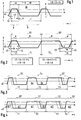
- Fig. 1 is a pulse-width modulated signal s0 with a relatively flat in the time diagram schematically Signal edges shown.
- the intersections of the signal edges with a mean signal level m, the transmitter side, the logical signal states H, L define form a first and second Signal part A, B of a single signal SO.
- the first signal part A corresponds to the time interval tA and the second signal part B the time interval tB.
- a switching threshold k defines which parts of the received Signal s0 are attributable to a first or second logic state H ', L'. Is this one? Switching threshold k no longer at the middle signal level m, then sender and vote On the receiver side, the logic levels H, L or H ', L' no longer coincide and the finite Slope of the signal edges occurs a distortion of the time intervals for signal parts A, B in Receiver on. Instead of the right time tA is now only the time for the first signal part A. t2, which is shorter than the interval tA by the time intervals t3, t4. Correspondingly enlarged the interval tB of the second signal part B by the intervals t3, t4.
- Pulse width ratio on the receiver side is expediently only one of the two Signal parts A, B and the period T used, since the latter by the position of the switching threshold k is not affected.
- the sum of the intervals t3, t4 gives the phase error td.
- FIG. 2 shows a first exemplary embodiment of the invention with reference to the pulse-width-modulated signal s1 in the time diagram.
- the single signal SO of FIG. 1 corresponds to this Single signal S1, which is not inverted during a first period T1 and during a second Period T2 inverted as a single signal S1 'is transmitted.
- the first signal part A at the signal S1 thereby by the intervals t3, t4 smaller than the correct interval tA.
- In the inverted transmission is the time interval t5 for the first signal part A 'by the intervals t3, t4 greater than the correct one Interval tA.
- the order of the first and second signal part A, B is in Fig. 2 in the two periods T1, T2 interchanged. In this way, the non-inverted and the inverted signal match edge together, see the rising signal edge between the signal parts B, B '.
- Fig. 3 are in the time chart as a further embodiment of the invention three successive clock periods of a pulse width modulated signal s2 shown.
- a first individual signal S1 is transmitted.
- a second individual signal Sx is transmitted, which has a pulse width ratio of about 0.5 Has. Whose first and second signal part Ax, Bx are about the same length. If this relationship with real measured values does not occur, then this pulse width ratio can serve as a separation signal.
- the receiver knows that the first individual signal S1 comes again after the separation signal Sx, but in inverted form S1 '. Thereafter, a new single signal is expected, to which a separation signal Sx follows and then the inversion of the previously received single signal.
- the order of incoming individual signals is so clearly defined.
- the separation signals be inserted elsewhere in the signal curve s2, so that, for example, a separation after associated individual signals and the signal pairs are not separated.
- a pulse width modulated signal s3 is shown in the time chart, the determination of the Phase error td is used.
- the first period T1 an inverted individual signal S1 'with the Signal parts B1 'and A1' and then transmit the associated non-inverted single signal S1 with the signal parts A1, B1.
- the phase error td in the receiver determined, which then in the detection of the further individual signals S2, S3 in the periods T3, T4 for Correction of the time intervals of the first signal parts A2, A3 is used.
Landscapes
- Engineering & Computer Science (AREA)
- Signal Processing (AREA)
- Physics & Mathematics (AREA)
- Theoretical Computer Science (AREA)
- General Physics & Mathematics (AREA)
- Spectroscopy & Molecular Physics (AREA)
- Computer Networks & Wireless Communication (AREA)
- Multimedia (AREA)
- Arrangements For Transmission Of Measured Signals (AREA)
Abstract
Description
Claims (12)
- Sensorausgangssignal, das mittels eines pulsweitenmodulierten Signals (s1; s2; s3) den momentanen Wert eines Meßsignals in kodierter Form enthält, wobei der momentane Wert einem zeitlichen Verhältnis aus einem ersten und zweiten Signalteil (A, B) entspricht, die sich durch einen ersten bzw. zweiten logischen Zustand (H, L) voneinander unterscheiden, dadurch gekennzeichnet, daß
mindestens einmal während eines Meßablaufs ein bereits abgegebener Meßwert, ein nichtinvertiertes Einzelsignal (S1), mit einer invertierten Kodierung als ein invertiertes Einzelsignal (S1') nochmals abgegeben wird, wobei der erste Signalteil (A) mit dem zweiten logischen Zustand (L)und der zweite Signalteil (B) mit dem ersten logischen Zustand (H) verknüpft wird. - Sensorausgangssignal nach Anspruch 1, dadurch gekennzeichnet, daß das zeitliche Verhältnis auf einen konstanten Zeitwert (T) bezogen ist.
- Sensorausgangssignal nach Anspruch 2, dadurch gekennzeichnet, daß der konstante Zeitwert mit einer Taktperiode ( T) verknüpft ist.
- Sensorausgangssignal nach Anspruch 3, dadurch gekennzeichnet, daß die Taktperiode (T) im pulsweitenmodulierten Signal (s1; s2; s3) enthalten ist.
- Sensorausgangssignal nach Anspruch 1, dadurch gekennzeichnet, daß jeder Meßwert mindestens einmal als nichtinvertiertes Einzelsignal (S1) und mindestens einmal als invertiertes Einzelsignal (S1') abgegeben wird, wobei die Reihenfolge beliebig ist.
- Sensorausgangssignal nach Anspruch 5, dadurch gekennzeichnet, daß bei den alternierend erzeugten nichtinvertierten und invertierten Einzelsignalen (S1, S1') die jeweilige Reihenfolge aus dem erstem und zweitem Signalteil (A, B bzw. B', A') vertauscht wird.
- Sensorausgangssignal nach Anspruch 1, dadurch gekennzeichnet, daß zu Beginn des Meßablaufs ein Messwert oder ein fester Referenzwert in normaler und invertierter Kodierung als ein Einzelsignal (S1, S1') abgegeben wird, aus dem empfängerseitig ein Phasenfehler (td) bestimmt und gespeichert wird, der nachfolgenden Einzelsignalen (S2, S3) als Korrekturwert dient.
- Sensorausgangssignal nach einem der Ansprüche 1 bis 7, dadurch gekennzeichnet, daß in dem Meßablauf mindestens ein erstes Trennsignal (Sx) vorhanden ist, das empfängerseitig eine einfache Unterscheidung zwischen nichtinvertierten und invertierten Einzelsignalen (S1, S1') ermöglicht.
- Sensorausgangssignal nach einem der Ansprüche 1 bis 8, dadurch gekennzeichnet, daß in dem Meßablauf mindestens ein zweites Trennsignal vorhanden ist, mit dem während des Meßablaufs das Ende oder der Beginn eines neuen Einzelsignals signalisiert wird.
- Sensorausgangssignal nach Anspruch 1, dadurch gekennzeichnet, daß während der Übertragung des invertierten Ausgangssignals im Sensor ein Systemtest erfolgt, dessen Ergebnis während des Meßablaufes mittels eines Einzelsignals (S1, S2, S3) übertragen wird.
- Sensorausgangssignal nach einem der Ansprüche 1 bis 10, dadurch gekennzeichnet, daß der erste und zweite logische Zustand (H, L) durch unterschiedliche Strompegel definiert sind.
- Sensorausgangssignal nach Anspruch 11, dadurch gekennzeichnet, daß die unterschiedlichen Strompegel an den Versorgungsanschlüssen eines Zweibeinelementes abgreifbar sind.
Applications Claiming Priority (2)
| Application Number | Priority Date | Filing Date | Title |
|---|---|---|---|
| DE2002120844 DE10220844B4 (de) | 2002-05-08 | 2002-05-08 | Verfahren zur Übertragung von Messwerten mittels eines pulsmodulierten Signals sowie zugehöriger Sensor und System mit Sensor |
| DE10220844 | 2002-05-08 |
Publications (2)
| Publication Number | Publication Date |
|---|---|
| EP1363404A1 true EP1363404A1 (de) | 2003-11-19 |
| EP1363404B1 EP1363404B1 (de) | 2014-04-09 |
Family
ID=29265213
Family Applications (1)
| Application Number | Title | Priority Date | Filing Date |
|---|---|---|---|
| EP20030010032 Expired - Lifetime EP1363404B1 (de) | 2002-05-08 | 2003-05-02 | Pulsweitenmoduliertes Sensorausgangssignal |
Country Status (2)
| Country | Link |
|---|---|
| EP (1) | EP1363404B1 (de) |
| DE (1) | DE10220844B4 (de) |
Cited By (1)
| Publication number | Priority date | Publication date | Assignee | Title |
|---|---|---|---|---|
| EP3032223A1 (de) * | 2014-12-09 | 2016-06-15 | National Chung Shan Institute of Science and Technology | Kontaktloser einstellbarer hysteretischer magnetischer Codierer |
Citations (3)
| Publication number | Priority date | Publication date | Assignee | Title |
|---|---|---|---|---|
| DE19734248A1 (de) * | 1997-08-07 | 1999-02-11 | Litef Gmbh | Verfahren und Einrichtung zur Übertragung von Sensorausgangssignalen zwischen asynchron arbeitenden Sensoren und ihren jeweiligen Datenverarbeitungseinrichtungen |
| DE19737999A1 (de) * | 1997-08-30 | 1999-03-04 | Bosch Gmbh Robert | Einrichtung zur Winkelerfassung und Winkelzuordnung |
| GB2332835A (en) * | 1997-12-24 | 1999-06-30 | Daewoo Electronics Co Ltd | Differential post-coder for a tcm decoder |
-
2002
- 2002-05-08 DE DE2002120844 patent/DE10220844B4/de not_active Expired - Lifetime
-
2003
- 2003-05-02 EP EP20030010032 patent/EP1363404B1/de not_active Expired - Lifetime
Patent Citations (3)
| Publication number | Priority date | Publication date | Assignee | Title |
|---|---|---|---|---|
| DE19734248A1 (de) * | 1997-08-07 | 1999-02-11 | Litef Gmbh | Verfahren und Einrichtung zur Übertragung von Sensorausgangssignalen zwischen asynchron arbeitenden Sensoren und ihren jeweiligen Datenverarbeitungseinrichtungen |
| DE19737999A1 (de) * | 1997-08-30 | 1999-03-04 | Bosch Gmbh Robert | Einrichtung zur Winkelerfassung und Winkelzuordnung |
| GB2332835A (en) * | 1997-12-24 | 1999-06-30 | Daewoo Electronics Co Ltd | Differential post-coder for a tcm decoder |
Non-Patent Citations (1)
| Title |
|---|
| HIORNS R E ET AL: "POWER DIGITAL TO ANALOGUE WIDT MODULATION AND DIGITAL SIGNAL PROCESSING", IEE PROCEEDINGS G. ELECTRONIC CIRCUITS & SYSTEMS, INSTITUTION OF ELECTRICAL ENGINEERS. STEVENAGE, GB, vol. 140, no. 5, 1 October 1993 (1993-10-01), pages 329 - 338, XP000400068, ISSN: 0622-0039 * |
Cited By (1)
| Publication number | Priority date | Publication date | Assignee | Title |
|---|---|---|---|---|
| EP3032223A1 (de) * | 2014-12-09 | 2016-06-15 | National Chung Shan Institute of Science and Technology | Kontaktloser einstellbarer hysteretischer magnetischer Codierer |
Also Published As
| Publication number | Publication date |
|---|---|
| EP1363404B1 (de) | 2014-04-09 |
| DE10220844B4 (de) | 2006-05-11 |
| DE10220844A1 (de) | 2003-12-18 |
Similar Documents
| Publication | Publication Date | Title |
|---|---|---|
| DE3221499A1 (de) | Verfahren und schaltungsanordnung zur automatischen erfassung der spitzenwerte eines unbekannten elektrischen signals | |
| EP0051141B1 (de) | Verfahren und Einrichtung zur Entzerrung binärer Empfangssignale | |
| EP0232451A1 (de) | Verfahren und Einrichtung zur Umwandlung eines elektrischen Signals in eine proportionale Frequenz | |
| DE3533467C2 (de) | Verfahren und Anordnung zum störsicheren Erkennen von in Datensignalen enthaltenen Daten | |
| EP0332642B1 (de) | Verfahren und schaltungsanordnung zur adaptiven entzerrung von impulssignalen | |
| EP1363404B1 (de) | Pulsweitenmoduliertes Sensorausgangssignal | |
| DE1762267A1 (de) | Impulsbreitendiskriminator | |
| WO1988003733A2 (en) | Process and circuit for adaptive correction of pulsed signals | |
| DE2719223C2 (de) | Anordnung zum Umsetzen von Alarmsignalen zwischen einem digitalen Nachrichtenübertragungssystem und einer zentralen Betriebsüberwachung | |
| DE3608440C2 (de) | ||
| DE2613930B2 (de) | Digitaler Phasenregelkreis | |
| DE2729108C3 (de) | Schaltungsanordnung zur Erkennung von Taktsignalen und zur Umwandlung in digitale Dauersignale | |
| DE2442822C3 (de) | Schaltungsanordnung zur Messung von auf Datenubertragungsstrecken auftretenden Pegelunterbrechungen und Pegelabsenkungen | |
| DE3239935C2 (de) | Schaltungsanordnung zum Umwandeln eines mit Prellungen behafteten Eingangssignales in prellfreie Ausgangssignale | |
| DE2333571A1 (de) | Demodulator fuer frequenzmodulierte signale | |
| EP0016256B1 (de) | Schaltungsanordnung zum Korrigieren von Schrittverzerrungen bei einer Übertragung von Daten mit Frequenzmodulation | |
| DE2335296C2 (de) | Schaltungsanordnung zum Begrenzen der Schrittgeschwindigkeit bei einer Übertragung von Daten | |
| DE2002564C3 (de) | Empfänger für eine Fernmeßanordnung | |
| DE2010536C (de) | Detektor für frequenzmodulierte Signale | |
| DE1922529C (de) | Verfahren und Vorrichtung zur Auswertung von durch Impulse zeitlich begrenzten Intervallen | |
| DE4212751A1 (de) | Verfahren und Schaltungsanordnung zur Messung der elektromagnetischen Verträglichkeit digitaler Baugruppen | |
| DE1673730C (de) | Empfängeruhr | |
| DE3028582C2 (de) | Informationsübertragungseinrichtung, bei der ein Abfragesignal frequenzselektiv reflektiert wird | |
| DE19843980B4 (de) | Schaltungsanordnung zur Unterdrückung von einem digitalen Signal überlagerten Störimpulsen | |
| CH603012A5 (en) | Pulse train correction circuit |
Legal Events
| Date | Code | Title | Description |
|---|---|---|---|
| PUAI | Public reference made under article 153(3) epc to a published international application that has entered the european phase |
Free format text: ORIGINAL CODE: 0009012 |
|
| AK | Designated contracting states |
Kind code of ref document: A1 Designated state(s): AT BE BG CH CY CZ DE DK EE ES FI FR GB GR HU IE IT LI LU MC NL PT RO SE SI SK TR |
|
| AX | Request for extension of the european patent |
Extension state: AL LT LV MK |
|
| 17P | Request for examination filed |
Effective date: 20040519 |
|
| AKX | Designation fees paid |
Designated state(s): DE FR GB IT NL |
|
| 17Q | First examination report despatched |
Effective date: 20091116 |
|
| GRAP | Despatch of communication of intention to grant a patent |
Free format text: ORIGINAL CODE: EPIDOSNIGR1 |
|
| INTG | Intention to grant announced |
Effective date: 20131220 |
|
| GRAS | Grant fee paid |
Free format text: ORIGINAL CODE: EPIDOSNIGR3 |
|
| GRAA | (expected) grant |
Free format text: ORIGINAL CODE: 0009210 |
|
| AK | Designated contracting states |
Kind code of ref document: B1 Designated state(s): DE FR GB IT NL |
|
| REG | Reference to a national code |
Ref country code: GB Ref legal event code: FG4D Free format text: NOT ENGLISH |
|
| REG | Reference to a national code |
Ref country code: DE Ref legal event code: R096 Ref document number: 50315012 Country of ref document: DE Effective date: 20140515 |
|
| REG | Reference to a national code |
Ref country code: NL Ref legal event code: VDEP Effective date: 20140409 |
|
| PG25 | Lapsed in a contracting state [announced via postgrant information from national office to epo] |
Ref country code: NL Free format text: LAPSE BECAUSE OF FAILURE TO SUBMIT A TRANSLATION OF THE DESCRIPTION OR TO PAY THE FEE WITHIN THE PRESCRIBED TIME-LIMIT Effective date: 20140409 |
|
| REG | Reference to a national code |
Ref country code: DE Ref legal event code: R119 Ref document number: 50315012 Country of ref document: DE |
|
| PLBE | No opposition filed within time limit |
Free format text: ORIGINAL CODE: 0009261 |
|
| STAA | Information on the status of an ep patent application or granted ep patent |
Free format text: STATUS: NO OPPOSITION FILED WITHIN TIME LIMIT |
|
| REG | Reference to a national code |
Ref country code: DE Ref legal event code: R119 Ref document number: 50315012 Country of ref document: DE Effective date: 20141202 |
|
| 26N | No opposition filed |
Effective date: 20150112 |
|
| PG25 | Lapsed in a contracting state [announced via postgrant information from national office to epo] |
Ref country code: IT Free format text: LAPSE BECAUSE OF FAILURE TO SUBMIT A TRANSLATION OF THE DESCRIPTION OR TO PAY THE FEE WITHIN THE PRESCRIBED TIME-LIMIT Effective date: 20140409 |
|
| PG25 | Lapsed in a contracting state [announced via postgrant information from national office to epo] |
Ref country code: DE Free format text: LAPSE BECAUSE OF NON-PAYMENT OF DUE FEES Effective date: 20141202 |
|
| REG | Reference to a national code |
Ref country code: FR Ref legal event code: PLFP Year of fee payment: 14 |
|
| REG | Reference to a national code |
Ref country code: FR Ref legal event code: PLFP Year of fee payment: 15 |
|
| REG | Reference to a national code |
Ref country code: FR Ref legal event code: PLFP Year of fee payment: 16 |
|
| REG | Reference to a national code |
Ref country code: FR Ref legal event code: CD Owner name: TDK-MICRONAS GMBH, DE Effective date: 20180717 |
|
| PGFP | Annual fee paid to national office [announced via postgrant information from national office to epo] |
Ref country code: FR Payment date: 20190522 Year of fee payment: 17 |
|
| PGFP | Annual fee paid to national office [announced via postgrant information from national office to epo] |
Ref country code: GB Payment date: 20190521 Year of fee payment: 17 |
|
| GBPC | Gb: european patent ceased through non-payment of renewal fee |
Effective date: 20200502 |
|
| PG25 | Lapsed in a contracting state [announced via postgrant information from national office to epo] |
Ref country code: GB Free format text: LAPSE BECAUSE OF NON-PAYMENT OF DUE FEES Effective date: 20200502 Ref country code: FR Free format text: LAPSE BECAUSE OF NON-PAYMENT OF DUE FEES Effective date: 20200531 |