EP1363401A1 - Input buffers with common internal reference voltage - Google Patents
Input buffers with common internal reference voltage Download PDFInfo
- Publication number
- EP1363401A1 EP1363401A1 EP03009724A EP03009724A EP1363401A1 EP 1363401 A1 EP1363401 A1 EP 1363401A1 EP 03009724 A EP03009724 A EP 03009724A EP 03009724 A EP03009724 A EP 03009724A EP 1363401 A1 EP1363401 A1 EP 1363401A1
- Authority
- EP
- European Patent Office
- Prior art keywords
- input
- reference voltage
- control signal
- input buffers
- semiconductor device
- Prior art date
- Legal status (The legal status is an assumption and is not a legal conclusion. Google has not performed a legal analysis and makes no representation as to the accuracy of the status listed.)
- Granted
Links
Images


Classifications
-
- H—ELECTRICITY
- H03—ELECTRONIC CIRCUITRY
- H03K—PULSE TECHNIQUE
- H03K19/00—Logic circuits, i.e. having at least two inputs acting on one output; Inverting circuits
- H03K19/02—Logic circuits, i.e. having at least two inputs acting on one output; Inverting circuits using specified components
- H03K19/173—Logic circuits, i.e. having at least two inputs acting on one output; Inverting circuits using specified components using elementary logic circuits as components
- H03K19/1731—Optimisation thereof
- H03K19/1732—Optimisation thereof by limitation or reduction of the pin/gate ratio
-
- H—ELECTRICITY
- H03—ELECTRONIC CIRCUITRY
- H03K—PULSE TECHNIQUE
- H03K19/00—Logic circuits, i.e. having at least two inputs acting on one output; Inverting circuits
- H03K19/0175—Coupling arrangements; Interface arrangements
- H03K19/0185—Coupling arrangements; Interface arrangements using field effect transistors only
- H03K19/018507—Interface arrangements
- H03K19/018514—Interface arrangements with at least one differential stage
Definitions
- the present invention relates to a semiconductor device including a plurality of input buffers to which internally-generated reference voltages are applied.
- a plurality of input buffers are constructed by differential amplifiers for amplifying the difference between input voltages and respective reference voltages.
- the reference voltages are generated within the semiconductor device.
- the reference voltages are important parameters for determining whether the operation of the input buffers is normal or abnormal, i.e., whether the semiconductor device is normal or abnormal. Therefore, each of the input buffers monitors its reference voltage which is transmitted to an external pad in a test mode. This will be explained later in detail.
- the larger the number of input buffers the larger the number of external pads for monitored reference voltages.
- the semiconductor device constitutes a processor
- the number of input buffers is several hundreds.
- the semiconductor device including such input buffers would be increased in size.
- a semiconductor device is constructed by at least one reference voltage generating circuit for generating a reference voltage, a plurality of input voltage pads for receiving input voltages, a control signal pad for receiving a control signal, and a plurality of input buffers.
- Each of the input buffers amplifies a difference between one of the input voltages and the reference voltage to generate an output voltage, and includes a switch connected between the reference voltage generating circuit and one of the input voltage pads and controlled by the control signal.
- the reference voltage is transmitted by the control signal from the reference voltage generating circuit to the input voltage pads
- a plurality of input buffers such as input buffers 1, 2, ⁇ , 8 are provided.
- the input buffers 1, 2, 3 and 4 for the same interface receive input voltages IN 1 , IN 2 , IN 3 and IN 4 , respectively, so that the input voltages IN 1 , IN 2 , IN 3 and IN 4 are compared with a reference voltage V REFA generated from a voltage divider by resistors R A1 and R A2 .
- the input buffers 1, 2, 3 and 4 generate output voltages OUT 1 , OUT 2 , OUT 3 and OUT 4 in accordance with differences between the input voltages IN 1 , IN 2 , IN 3 and IN 4 and the reference voltage V REFA .
- the input buffers 5, 6, 7 and 8 for the same interface receive input voltages IN 5 , IN 6 , IN 7 and IN 8 respectively, so that the input voltages IN 5 , IN 6 , IN 7 and IN 8 are compared with a reference voltage V REFB generated from a voltage divider by resistors R B1 and R B2 .
- the input buffers 5, 6, 7 and 8 generate output voltages OUT 5 , OUT 6 , OUT 7 and OUT 8 in accordance with differences between the input voltages IN 5 , IN 6 , IN 7 and IN 8 and the reference voltage V REFB .
- V REFA or V REFB
- ECL emitter coupled logic
- the reference voltages MV REFA and MV REFB can be monitored, In this case, however, the layouts of the input buffers 1, 2, ⁇ , 8 are not uniform. In view of a semiconductor design rule that the layouts of the input buffers are all the same, the above-mentioned configuration in which the input buffers 1 and 5 are different from the other input buffers is not preferable.
- Fig. 3 which illustrates a first embodiment of the semiconductor device according to the present invention
- the input buffers 1, 2, 3, 4, 5, 6, 7 and 8 of Fig. 1 are replaced by input buffers 1', 2', 3', 4', 5', 6', 7' and 8' where the external pads for the monitored reference voltages MV REF1 , MV REF2 , MV REF3 , MV REF4 , MV REF5 , MV REF6 , MV REF7 and MV REF8 of Fig. 1 are replaced by a single external pad for a control signal CNT.
- the control signal CNT is made high, so that the transistor Q6 is turned ON. Therefore, the reference voltage V REFA (or V REFB ) is transmitted to the pads for the input voltages IN 1 , IN 2 , ⁇ , IN 8 , thus monitoring the reference voltage V REFA (or V REFB ).
- a P-channel MOS transistor Q7 as a switch is added to the elements of the input buffer i of Fig. 2.
- the control signal CNT is made low, so that the transistor Q7 is turned ON. Therefore, the reference voltage V REFA (or V REFB ) is transmitted to the pads for the input voltages IN 1 , IN 2 , ⁇ , IN 8 , thus monitoring the reference voltage V REFA (or V REFB ).
- a transfer gate T formed by a P-channel MOS transistor and an N-channel MOS transistor as a switch is added to the elements of the input buffer i of Fig. 2.
- the control signal CNT is made low, so that the transistor gate T is opened. Therefore, the reference voltage V REFA (or V REFB ) is transmitted to the pads for the input voltages IN 1 , IN 2 , ⁇ , IN 8 , thus monitoring the reference voltage V REFA (or V REFB ).
- the input buffer i' of Fig. 6 is increased in size as compared with those of Figs. 4 and 5; however, the input buffer i' of Fig. 6 has an advantage in that the monitored range of the reference voltage V REFA (or V REFB ) can be increased.
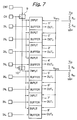
- Fig. 7 which illustrates a second embodiment of the semiconductor device according to the present invention
- registers i.e., D-type flip-flops 9 and 10 connected in series and a pad for a clock signal CK for the D-type flip-flops 9 and 10 are added to the elements of Fig. 3. That is, the D-type flip-flops 9 and 10 store the control signal CNT in synchronization with the clock signal CK.
- the switches within the input buffers 1', 2', 3' and 4' are turned OFF, so that the input buffers 1', 2', 3' and 4' normally operate, while the switches within the input buffers 5', 6', 7' and 8' are turned ON, so that the reference voltage V REFB is transmitted to the pads for the input voltages IN 5 , IN 6 , IN 7 and IN 8 , thus performing a reference voltage monitoring operation upon the reference voltage V REFB .
- the switches within the input buffers 1', 2', 3' and 4' are turned ON, so that the reference voltage V REFA is transmitted to the pads for the input voltages IN 1 , IN 2 , IN 3 and IN 4 , thus performing a reference voltage monitoring operation upon the reference voltage V REFA , while the switches within the input buffers 5', 6', 7' and 8' are turned OFF, so that the input buffers 5', 6', 7' and 8' normally operate.
- the switches within the input buffers 1', 2', 3', 4', 5', 6', 7' and 8' are turned ON, so that the reference voltage V REFA is transmitted to the pads for the input voltages IN 1 , IN 2 , IN 3 and IN 4 , thus performing a reference voltage monitoring operation upon the reference voltage V REFA and simultaneously, the switches within the input buffers 5', 6', 7' and 8' are turned ON, so that the reference voltage V REFB is transmitted to the pads for the input voltages IN 5 , IN 6 , IN 7 and IN 8 thus performing a reference voltage monitoring operation upon the reference voltage V REFB .
- the transistors Q1 and Q2 can be of a P-channel type and the transistors Q3, Q4 and Q5 can be of an N-channel type, as illustrated in Fig. 8 which corresponds to Fig. 4.
- the voltage dividers can be constructed by a series of P-channel MOS transistors whose gates are connected to a high power supply voltage terminal or a series of N-channel MOS transistors whose gates are connected to a low power supply voltage terminal.
- the semiconductor device can be decreased in size.
Abstract
Description
- The present invention relates to a semiconductor device including a plurality of input buffers to which internally-generated reference voltages are applied.
- Generally, in a semiconductor device, a plurality of input buffers are constructed by differential amplifiers for amplifying the difference between input voltages and respective reference voltages. Also, in order to decrease the number of external pads, the reference voltages are generated within the semiconductor device. In this case, the reference voltages are important parameters for determining whether the operation of the input buffers is normal or abnormal, i.e., whether the semiconductor device is normal or abnormal. Therefore, each of the input buffers monitors its reference voltage which is transmitted to an external pad in a test mode. This will be explained later in detail.
- In the above-described prior art semiconductor device, however, the larger the number of input buffers, the larger the number of external pads for monitored reference voltages. For example, if the semiconductor device constitutes a processor, the number of input buffers is several hundreds. As a result, the semiconductor device including such input buffers would be increased in size.
- It is an object of the present invention to provide a semiconductor device having a plurality of input buffers with a reduced number of external pads.
- According to the present invention, a semiconductor device is constructed by at least one reference voltage generating circuit for generating a reference voltage, a plurality of input voltage pads for receiving input voltages, a control signal pad for receiving a control signal, and a plurality of input buffers. Each of the input buffers amplifies a difference between one of the input voltages and the reference voltage to generate an output voltage, and includes a switch connected between the reference voltage generating circuit and one of the input voltage pads and controlled by the control signal.
- Thus, the reference voltage is transmitted by the control signal from the reference voltage generating circuit to the input voltage pads
- The present invention will be more clearly understood from the description set forth below, as compared with the prior art, with reference to the accompanying drawings, wherein:
- Fig. 1 is a block circuit diagram illustrating a prior art semiconductor device;
- Fig. 2 is a detailed circuit diagram of the input buffer of Fig. 1;
- Fig. 3 is a block circuit diagram illustrating a first embodiment of the semiconductor device according to the present invention;
- Fig. 4 is a detailed circuit diagram of the input buffer of Fig. 3;
- Figs 5 and 6 are circuit diagrams illustrating modifications of the input buffer of Fig. 4;
- Fig. 7 is a block circuit diagram illustrating a second embodiment of the semiconductor device according to the present invention;
- Fig. 8 is a circuit diagram illustrating a modification of the input buffer of Figs. 4 and 6;
-
- Before the description of the preferred embodiments, a prior art semiconductor device will be explained with reference to Figs. 1 and 2.
- In Fig. 1, which illustrates a prior art semiconductor device, a plurality of input buffers such as
input buffers - For example, the
input buffers input buffers - Similarly, the
input buffers input buffers - Since the reference voltages VREFA and VREFB are generated within the semiconductor device, each of the
input buffers - In Fig. 2, which is a detailed circuit diagram of the input buffer i (= 1, 2, ···, 8) of Fig. 1, the input buffer i is constructed by N-channel MOS transistors Q1 and Q2 forming a current mirror circuit, P-channel MOS transistors Q3 and Q4 whose gates receive the input voltage INi and the reference voltage VREFA (or VREFB), and a P-
channel 1 MOS transistor Q5 serving as a current source. Therefore, the input buffer i amplifies the difference between the input voltage INi and the reference voltage VREFA (or VREFB) to generate the output voltage OUT; in response to this difference. For example, the input voltage INi of an emitter coupled logic (ECL) level whose amplitude is small is converted into the output voltage OUTi of a CMOS level whose amplitude is large. - In Figs. 1 and 2, however, the larger the number of input buffers, the larger the number of external pads for monitored reference voltages MVREF1, MVREF2, ···. Therefore, a semiconductor device including such input buffers is increased in size.
- In Figs. 1 and 2, even if only the pads for the monitored reference voltages MVREF1 and MVREF5 are provided and the pads for the monitored reference voltage MVREF2, MVREF3, MVREF4, MVREF6, MVREF7 and MVREF8 are not provided, the reference voltages MVREFA and MVREFB can be monitored, In this case, however, the layouts of the
input buffers input buffers - In Fig. 3, which illustrates a first embodiment of the semiconductor device according to the present invention, the
input buffers - In Fig. 4, which is a detailed circuit diagram of the input buffer i' (i' = 1, 2, ···, 8) of Fig. 3, an N-channel MOS transistor Q6 as a switch is added to the elements of the input buffer i of Fig. 2.
- In a normal operation mode, the control signal CNT is made low, so that the transistor Q6 is turned OFF. Therefore, the input buffer i' (i' = 1, 2, ···, 8) operates normally.
- In a reference voltage monitoring mode, the control signal CNT is made high, so that the transistor Q6 is turned ON. Therefore, the reference voltage VREFA (or VREFB) is transmitted to the pads for the input voltages IN1, IN2, ···, IN8, thus monitoring the reference voltage VREFA (or VREFB).
- In Fig. 5, which is a modification of the input buffer i' (i' = 1, 2, ···, 8) of Fig. 4, a P-channel MOS transistor Q7 as a switch is added to the elements of the input buffer i of Fig. 2.
- In a normal operation mode, the control signal CNT is made high, so that the transistor Q7 is turned OFF. Therefore, the input buffer i' (i' = 1, 2, ···, 8) operates normally.
- In a reference voltage monitoring mode, the control signal CNT is made low, so that the transistor Q7 is turned ON. Therefore, the reference voltage VREFA (or VREFB) is transmitted to the pads for the input voltages IN1, IN2, ···, IN8, thus monitoring the reference voltage VREFA (or VREFB).
- In Fig. 6, which is another modification of the input buffer i' (i' = 1, 2, ···, 8) of Fig. 4, a transfer gate T formed by a P-channel MOS transistor and an N-channel MOS transistor as a switch is added to the elements of the input buffer i of Fig. 2.
- In a normal operation mode, the control signal CNT is made high, so that the transistor gate T is closed. Therefore, the input buffer i' (i' = 1, 2, ···, 8) operates normally.
- In a reference voltage monitoring mode, the control signal CNT is made low, so that the transistor gate T is opened. Therefore, the reference voltage VREFA (or VREFB) is transmitted to the pads for the input voltages IN1, IN2, ···, IN8, thus monitoring the reference voltage VREFA (or VREFB).
- The input buffer i' of Fig. 6 is increased in size as compared with those of Figs. 4 and 5; however, the input buffer i' of Fig. 6 has an advantage in that the monitored range of the reference voltage VREFA (or VREFB) can be increased.
- In Fig. 7, which illustrates a second embodiment of the semiconductor device according to the present invention, registers, i.e., D-type flip-
flops 9 and 10 connected in series and a pad for a clock signal CK for the D-type flip-flops 9 and 10 are added to the elements of Fig. 3. That is, the D-type flip-flops 9 and 10 store the control signal CNT in synchronization with the clock signal CK. - If "0" is stored in the D-type flip-
flops 9 and 10, the switches within the input buffers 1', 2', 3', 4', 5', 6', 7' and 8' are turned OFF, so that the input buffers 1', 2', 3', 4', 5', 6', 7' and 8' normally operate. - If "0" and "1" are stored in the D-type flip-
flops 9 and 10, respectively, the switches within the input buffers 1', 2', 3' and 4' are turned OFF, so that the input buffers 1', 2', 3' and 4' normally operate, while the switches within the input buffers 5', 6', 7' and 8' are turned ON, so that the reference voltage VREFB is transmitted to the pads for the input voltages IN5, IN6, IN7 and IN8, thus performing a reference voltage monitoring operation upon the reference voltage VREFB. - If "1" and "0" are stored in the D-type flip-
flops 9 and 10, respectively, the switches within the input buffers 1', 2', 3' and 4' are turned ON, so that the reference voltage VREFA is transmitted to the pads for the input voltages IN1, IN2, IN3 and IN4, thus performing a reference voltage monitoring operation upon the reference voltage VREFA, while the switches within the input buffers 5', 6', 7' and 8' are turned OFF, so that the input buffers 5', 6', 7' and 8' normally operate. - If "1" is stored in the D-type flip-
flops 9 and 10, the switches within the input buffers 1', 2', 3', 4', 5', 6', 7' and 8' are turned ON, so that the reference voltage VREFA is transmitted to the pads for the input voltages IN1, IN2, IN3 and IN4, thus performing a reference voltage monitoring operation upon the reference voltage VREFA and simultaneously, the switches within the input buffers 5', 6', 7' and 8' are turned ON, so that the reference voltage VREFB is transmitted to the pads for the input voltages IN5, IN6, IN7 and IN8 thus performing a reference voltage monitoring operation upon the reference voltage VREFB. - In Figs. 3 and 7, the number of pads for monitored reference voltages is decreased as compared with that of Fig. 1.
- In the above-described embodiments, the transistors Q1 and Q2 can be of a P-channel type and the transistors Q3, Q4 and Q5 can be of an N-channel type, as illustrated in Fig. 8 which corresponds to Fig. 4. Also, in Fig. 3, the voltage dividers can be constructed by a series of P-channel MOS transistors whose gates are connected to a high power supply voltage terminal or a series of N-channel MOS transistors whose gates are connected to a low power supply voltage terminal.
- As explained hereinabove, according to the present invention, since the number of pads for monitoring internally-generated reference vollages is decreased, the semiconductor device can be decreased in size.
Claims (6)
- A semiconductor device comprising:at least one reference voltage generating circuit (RA1, RA2; RB1, RB2) for generating a reference voltage (VREFA, VREFB);a plurality of input voltage pads for receiving input voltages (IN1, IN2, ···, IN8);a control signal pad for receiving a control signal (CNT);a plurality of input buffers (1', 2', ···, 8'), each connected to said control signal pad and one of said input voltage pads, each of said input buffers amplifying a difference between one of said input voltages and said reference voltage to generate an output voltage (OUT1, OUT2, ···, OUT8),each of said input buffers comprising a switch (Q6, Q7, T) connected between said reference voltage generating circuit and one of said input voltage pads and controlled by said control signal.
- The semiconductor device as set forth in claim 1, wherein said switch comprises an N-channel MOS transistor (Q6).
- The semiconductor device as set forth in claim 1 or 2, wherein said switch comprises a P-channel MOS transistor (Q7).
- The semiconductor device as set forth in claim 1, 2 or 3, wherein said switch comprises a transfer gate (T).
- The semiconductor device as set forth in claim 1, 2, 3 or 4 comprising a register (9, 10), connected between said control signal pad and said input buffers, for storing said control signal.
- The semiconductor device as set forth in claim 5, further comprising a clock signal pad for receiving a clock signal (CK),said register comprising a D-type flip-flop having a data terminal connected to said control signal pad, a clock terminal connected to said clock signal pad and an output terminal connected to said input buffers.
Applications Claiming Priority (2)
| Application Number | Priority Date | Filing Date | Title |
|---|---|---|---|
| JP2002140243A JP3876760B2 (en) | 2002-05-15 | 2002-05-15 | Input buffer circuit and semiconductor integrated circuit device |
| JP2002140243 | 2002-05-15 |
Publications (2)
| Publication Number | Publication Date |
|---|---|
| EP1363401A1 true EP1363401A1 (en) | 2003-11-19 |
| EP1363401B1 EP1363401B1 (en) | 2005-06-29 |
Family
ID=29267795
Family Applications (1)
| Application Number | Title | Priority Date | Filing Date |
|---|---|---|---|
| EP03009724A Expired - Fee Related EP1363401B1 (en) | 2002-05-15 | 2003-04-30 | Semiconductor device with input buffers with common internal reference voltage |
Country Status (4)
| Country | Link |
|---|---|
| US (1) | US6828829B2 (en) |
| EP (1) | EP1363401B1 (en) |
| JP (1) | JP3876760B2 (en) |
| DE (1) | DE60300910T2 (en) |
Cited By (1)
| Publication number | Priority date | Publication date | Assignee | Title |
|---|---|---|---|---|
| EP2412246A1 (en) | 2010-07-28 | 2012-02-01 | Bühler AG | Grinding coffee beans |
Families Citing this family (5)
| Publication number | Priority date | Publication date | Assignee | Title |
|---|---|---|---|---|
| KR100753032B1 (en) * | 2004-07-14 | 2007-08-30 | 주식회사 하이닉스반도체 | Input stage circuit |
| KR101893179B1 (en) * | 2012-01-31 | 2018-08-30 | 에스케이하이닉스 주식회사 | Receiver Circuit |
| US9792964B1 (en) * | 2016-09-20 | 2017-10-17 | Micron Technology, Inc. | Apparatus of offset voltage adjustment in input buffer |
| US11099774B2 (en) | 2017-08-30 | 2021-08-24 | Micron Technology, Inc. | Command address input buffer bias current reduction |
| KR102559563B1 (en) * | 2018-07-16 | 2023-07-26 | 에스케이하이닉스 주식회사 | Integrated circuit |
Citations (1)
| Publication number | Priority date | Publication date | Assignee | Title |
|---|---|---|---|---|
| JP2001267501A (en) * | 2000-03-16 | 2001-09-28 | Nec Eng Ltd | Semiconductor integrated circuit and testing method for input characteristics using the same |
Family Cites Families (5)
| Publication number | Priority date | Publication date | Assignee | Title |
|---|---|---|---|---|
| JPS60167517A (en) * | 1984-02-10 | 1985-08-30 | Hitachi Ltd | Voltage comparator |
| JPS62269512A (en) * | 1986-05-19 | 1987-11-24 | Nippon Telegr & Teleph Corp <Ntt> | Voltage comparator |
| JPH01166612A (en) * | 1987-12-23 | 1989-06-30 | Hitachi Ltd | Comparator |
| US4849661A (en) * | 1988-06-16 | 1989-07-18 | Intel Corporation | CMOS input buffer with switched capacitor reference voltage generator |
| JPH0247916A (en) * | 1988-08-08 | 1990-02-16 | Nec Corp | Analog comparator |
-
2002
- 2002-05-15 JP JP2002140243A patent/JP3876760B2/en not_active Expired - Fee Related
-
2003
- 2003-04-30 EP EP03009724A patent/EP1363401B1/en not_active Expired - Fee Related
- 2003-04-30 DE DE60300910T patent/DE60300910T2/en not_active Expired - Fee Related
- 2003-05-14 US US10/437,174 patent/US6828829B2/en not_active Expired - Fee Related
Patent Citations (1)
| Publication number | Priority date | Publication date | Assignee | Title |
|---|---|---|---|---|
| JP2001267501A (en) * | 2000-03-16 | 2001-09-28 | Nec Eng Ltd | Semiconductor integrated circuit and testing method for input characteristics using the same |
Non-Patent Citations (1)
| Title |
|---|
| PATENT ABSTRACTS OF JAPAN vol. 2000, no. 26 1 July 2002 (2002-07-01) * |
Cited By (2)
| Publication number | Priority date | Publication date | Assignee | Title |
|---|---|---|---|---|
| EP2412246A1 (en) | 2010-07-28 | 2012-02-01 | Bühler AG | Grinding coffee beans |
| WO2012013620A1 (en) | 2010-07-28 | 2012-02-02 | Bühler AG | Grinding of coffee beans |
Also Published As
| Publication number | Publication date |
|---|---|
| DE60300910D1 (en) | 2005-08-04 |
| JP3876760B2 (en) | 2007-02-07 |
| DE60300910T2 (en) | 2005-12-08 |
| US20030214328A1 (en) | 2003-11-20 |
| US6828829B2 (en) | 2004-12-07 |
| JP2003332902A (en) | 2003-11-21 |
| EP1363401B1 (en) | 2005-06-29 |
Similar Documents
| Publication | Publication Date | Title |
|---|---|---|
| US7345519B2 (en) | Flip-flop circuit | |
| US7358786B2 (en) | Control signal generator, latch circuit, flip flop and method for controlling operations of the flip-flop | |
| US7969194B2 (en) | Semiconductor device | |
| US5576651A (en) | Static/dynamic flip-flop | |
| US7859310B2 (en) | Semiconductor integrated circuit | |
| US7719319B2 (en) | Semiconductor integrated circuit | |
| US5298807A (en) | Buffer circuitry for transferring signals from TTL circuitry to dual range CMOS circuitry | |
| EP1363401B1 (en) | Semiconductor device with input buffers with common internal reference voltage | |
| JP4769509B2 (en) | Semiconductor device | |
| CN113608112A (en) | Scan output flip-flop | |
| US7501850B1 (en) | Scannable limited switch dynamic logic (LSDL) circuit | |
| US20210226628A1 (en) | Flip-flop device and method of operating flip-flop device | |
| CN106409342B (en) | Area efficient multi-bit flip-flop topology | |
| US5943274A (en) | Method and apparatus for amplifying a signal to produce a latched digital signal | |
| US7068079B2 (en) | Circuit device with clock pulse detection facility | |
| JP2697691B2 (en) | Semiconductor integrated circuit having scan path | |
| JP3057739B2 (en) | Semiconductor integrated circuit | |
| KR100339247B1 (en) | Comparator with 2-level test input | |
| KR100210858B1 (en) | Integrated circuit | |
| JPH05150003A (en) | Storage circuit | |
| JPH05300007A (en) | Two-input or circuit | |
| JP2656660B2 (en) | Semiconductor integrated circuit | |
| JP2947168B2 (en) | Semiconductor integrated circuit | |
| JPH05322984A (en) | Test input circuit | |
| JPH07134158A (en) | Output buffer circuit for mos semiconductor integrated circuit |
Legal Events
| Date | Code | Title | Description |
|---|---|---|---|
| PUAI | Public reference made under article 153(3) epc to a published international application that has entered the european phase |
Free format text: ORIGINAL CODE: 0009012 |
|
| AK | Designated contracting states |
Kind code of ref document: A1 Designated state(s): AT BE BG CH CY CZ DE DK EE ES FI FR GB GR HU IE IT LI LU MC NL PT RO SE SI SK TR |
|
| AX | Request for extension of the european patent |
Extension state: AL LT LV MK |
|
| 17P | Request for examination filed |
Effective date: 20031002 |
|
| GRAP | Despatch of communication of intention to grant a patent |
Free format text: ORIGINAL CODE: EPIDOSNIGR1 |
|
| GRAS | Grant fee paid |
Free format text: ORIGINAL CODE: EPIDOSNIGR3 |
|
| AKX | Designation fees paid |
Designated state(s): DE FR GB |
|
| RTI1 | Title (correction) |
Free format text: SEMICONDUCTOR DEVICE WITH INPUT BUFFERS WITH COMMON INTERNAL REFERENCE VOLTAGE |
|
| GRAA | (expected) grant |
Free format text: ORIGINAL CODE: 0009210 |
|
| AK | Designated contracting states |
Kind code of ref document: B1 Designated state(s): DE FR GB |
|
| REG | Reference to a national code |
Ref country code: GB Ref legal event code: FG4D |
|
| REF | Corresponds to: |
Ref document number: 60300910 Country of ref document: DE Date of ref document: 20050804 Kind code of ref document: P |
|
| ET | Fr: translation filed | ||
| PLBE | No opposition filed within time limit |
Free format text: ORIGINAL CODE: 0009261 |
|
| STAA | Information on the status of an ep patent application or granted ep patent |
Free format text: STATUS: NO OPPOSITION FILED WITHIN TIME LIMIT |
|
| 26N | No opposition filed |
Effective date: 20060330 |
|
| PGFP | Annual fee paid to national office [announced via postgrant information from national office to epo] |
Ref country code: DE Payment date: 20070426 Year of fee payment: 5 |
|
| PGFP | Annual fee paid to national office [announced via postgrant information from national office to epo] |
Ref country code: GB Payment date: 20070425 Year of fee payment: 5 |
|
| PGFP | Annual fee paid to national office [announced via postgrant information from national office to epo] |
Ref country code: FR Payment date: 20070411 Year of fee payment: 5 |
|
| GBPC | Gb: european patent ceased through non-payment of renewal fee |
Effective date: 20080430 |
|
| PG25 | Lapsed in a contracting state [announced via postgrant information from national office to epo] |
Ref country code: DE Free format text: LAPSE BECAUSE OF NON-PAYMENT OF DUE FEES Effective date: 20081101 |
|
| REG | Reference to a national code |
Ref country code: FR Ref legal event code: ST Effective date: 20081231 |
|
| PG25 | Lapsed in a contracting state [announced via postgrant information from national office to epo] |
Ref country code: FR Free format text: LAPSE BECAUSE OF NON-PAYMENT OF DUE FEES Effective date: 20080430 |
|
| PG25 | Lapsed in a contracting state [announced via postgrant information from national office to epo] |
Ref country code: GB Free format text: LAPSE BECAUSE OF NON-PAYMENT OF DUE FEES Effective date: 20080430 |