EP1363332A1 - Semiconductor device and method of manufacturing the same - Google Patents
Semiconductor device and method of manufacturing the same Download PDFInfo
- Publication number
- EP1363332A1 EP1363332A1 EP01906190A EP01906190A EP1363332A1 EP 1363332 A1 EP1363332 A1 EP 1363332A1 EP 01906190 A EP01906190 A EP 01906190A EP 01906190 A EP01906190 A EP 01906190A EP 1363332 A1 EP1363332 A1 EP 1363332A1
- Authority
- EP
- European Patent Office
- Prior art keywords
- trenches
- region
- trench
- impurity
- semiconductor device
- Prior art date
- Legal status (The legal status is an assumption and is not a legal conclusion. Google has not performed a legal analysis and makes no representation as to the accuracy of the status listed.)
- Granted
Links
Images










































Classifications
-
- H—ELECTRICITY
- H10—SEMICONDUCTOR DEVICES; ELECTRIC SOLID-STATE DEVICES NOT OTHERWISE PROVIDED FOR
- H10P—GENERIC PROCESSES OR APPARATUS FOR THE MANUFACTURE OR TREATMENT OF DEVICES COVERED BY CLASS H10
- H10P10/00—Bonding of wafers, substrates or parts of devices
-
- H—ELECTRICITY
- H10—SEMICONDUCTOR DEVICES; ELECTRIC SOLID-STATE DEVICES NOT OTHERWISE PROVIDED FOR
- H10D—INORGANIC ELECTRIC SEMICONDUCTOR DEVICES
- H10D30/00—Field-effect transistors [FET]
- H10D30/60—Insulated-gate field-effect transistors [IGFET]
- H10D30/64—Double-diffused metal-oxide semiconductor [DMOS] FETs
- H10D30/65—Lateral DMOS [LDMOS] FETs
- H10D30/657—Lateral DMOS [LDMOS] FETs having substrates comprising insulating layers, e.g. SOI-LDMOS transistors
-
- H—ELECTRICITY
- H10—SEMICONDUCTOR DEVICES; ELECTRIC SOLID-STATE DEVICES NOT OTHERWISE PROVIDED FOR
- H10D—INORGANIC ELECTRIC SEMICONDUCTOR DEVICES
- H10D30/00—Field-effect transistors [FET]
- H10D30/01—Manufacture or treatment
- H10D30/021—Manufacture or treatment of FETs having insulated gates [IGFET]
- H10D30/028—Manufacture or treatment of FETs having insulated gates [IGFET] of double-diffused metal oxide semiconductor [DMOS] FETs
- H10D30/0291—Manufacture or treatment of FETs having insulated gates [IGFET] of double-diffused metal oxide semiconductor [DMOS] FETs of vertical DMOS [VDMOS] FETs
-
- H—ELECTRICITY
- H10—SEMICONDUCTOR DEVICES; ELECTRIC SOLID-STATE DEVICES NOT OTHERWISE PROVIDED FOR
- H10D—INORGANIC ELECTRIC SEMICONDUCTOR DEVICES
- H10D30/00—Field-effect transistors [FET]
- H10D30/60—Insulated-gate field-effect transistors [IGFET]
- H10D30/64—Double-diffused metal-oxide semiconductor [DMOS] FETs
- H10D30/65—Lateral DMOS [LDMOS] FETs
- H10D30/655—Lateral DMOS [LDMOS] FETs having edge termination structures
-
- H—ELECTRICITY
- H10—SEMICONDUCTOR DEVICES; ELECTRIC SOLID-STATE DEVICES NOT OTHERWISE PROVIDED FOR
- H10D—INORGANIC ELECTRIC SEMICONDUCTOR DEVICES
- H10D30/00—Field-effect transistors [FET]
- H10D30/60—Insulated-gate field-effect transistors [IGFET]
- H10D30/64—Double-diffused metal-oxide semiconductor [DMOS] FETs
- H10D30/66—Vertical DMOS [VDMOS] FETs
- H10D30/665—Vertical DMOS [VDMOS] FETs having edge termination structures
-
- H—ELECTRICITY
- H10—SEMICONDUCTOR DEVICES; ELECTRIC SOLID-STATE DEVICES NOT OTHERWISE PROVIDED FOR
- H10D—INORGANIC ELECTRIC SEMICONDUCTOR DEVICES
- H10D62/00—Semiconductor bodies, or regions thereof, of devices having potential barriers
- H10D62/01—Manufacture or treatment
- H10D62/051—Forming charge compensation regions, e.g. superjunctions
- H10D62/058—Forming charge compensation regions, e.g. superjunctions by using trenches, e.g. implanting into sidewalls of trenches or refilling trenches
-
- H—ELECTRICITY
- H10—SEMICONDUCTOR DEVICES; ELECTRIC SOLID-STATE DEVICES NOT OTHERWISE PROVIDED FOR
- H10D—INORGANIC ELECTRIC SEMICONDUCTOR DEVICES
- H10D62/00—Semiconductor bodies, or regions thereof, of devices having potential barriers
- H10D62/10—Shapes, relative sizes or dispositions of the regions of the semiconductor bodies; Shapes of the semiconductor bodies
- H10D62/102—Constructional design considerations for preventing surface leakage or controlling electric field concentration
- H10D62/103—Constructional design considerations for preventing surface leakage or controlling electric field concentration for increasing or controlling the breakdown voltage of reverse-biased devices
- H10D62/105—Constructional design considerations for preventing surface leakage or controlling electric field concentration for increasing or controlling the breakdown voltage of reverse-biased devices by having particular doping profiles, shapes or arrangements of PN junctions; by having supplementary regions, e.g. junction termination extension [JTE]
- H10D62/106—Constructional design considerations for preventing surface leakage or controlling electric field concentration for increasing or controlling the breakdown voltage of reverse-biased devices by having particular doping profiles, shapes or arrangements of PN junctions; by having supplementary regions, e.g. junction termination extension [JTE] having supplementary regions doped oppositely to or in rectifying contact with regions of the semiconductor bodies, e.g. guard rings with PN or Schottky junctions
-
- H—ELECTRICITY
- H10—SEMICONDUCTOR DEVICES; ELECTRIC SOLID-STATE DEVICES NOT OTHERWISE PROVIDED FOR
- H10D—INORGANIC ELECTRIC SEMICONDUCTOR DEVICES
- H10D62/00—Semiconductor bodies, or regions thereof, of devices having potential barriers
- H10D62/10—Shapes, relative sizes or dispositions of the regions of the semiconductor bodies; Shapes of the semiconductor bodies
- H10D62/102—Constructional design considerations for preventing surface leakage or controlling electric field concentration
- H10D62/103—Constructional design considerations for preventing surface leakage or controlling electric field concentration for increasing or controlling the breakdown voltage of reverse-biased devices
- H10D62/105—Constructional design considerations for preventing surface leakage or controlling electric field concentration for increasing or controlling the breakdown voltage of reverse-biased devices by having particular doping profiles, shapes or arrangements of PN junctions; by having supplementary regions, e.g. junction termination extension [JTE]
- H10D62/109—Reduced surface field [RESURF] PN junction structures
- H10D62/111—Multiple RESURF structures, e.g. double RESURF or 3D-RESURF structures
-
- H—ELECTRICITY
- H10—SEMICONDUCTOR DEVICES; ELECTRIC SOLID-STATE DEVICES NOT OTHERWISE PROVIDED FOR
- H10D—INORGANIC ELECTRIC SEMICONDUCTOR DEVICES
- H10D62/00—Semiconductor bodies, or regions thereof, of devices having potential barriers
- H10D62/10—Shapes, relative sizes or dispositions of the regions of the semiconductor bodies; Shapes of the semiconductor bodies
- H10D62/113—Isolations within a component, i.e. internal isolations
- H10D62/115—Dielectric isolations, e.g. air gaps
- H10D62/116—Dielectric isolations, e.g. air gaps adjoining the input or output regions of field-effect devices, e.g. adjoining source or drain regions
-
- H—ELECTRICITY
- H10—SEMICONDUCTOR DEVICES; ELECTRIC SOLID-STATE DEVICES NOT OTHERWISE PROVIDED FOR
- H10D—INORGANIC ELECTRIC SEMICONDUCTOR DEVICES
- H10D62/00—Semiconductor bodies, or regions thereof, of devices having potential barriers
- H10D62/10—Shapes, relative sizes or dispositions of the regions of the semiconductor bodies; Shapes of the semiconductor bodies
- H10D62/13—Semiconductor regions connected to electrodes carrying current to be rectified, amplified or switched, e.g. source or drain regions
- H10D62/141—Anode or cathode regions of thyristors; Collector or emitter regions of gated bipolar-mode devices, e.g. of IGBTs
- H10D62/142—Anode regions of thyristors or collector regions of gated bipolar-mode devices
-
- H—ELECTRICITY
- H10—SEMICONDUCTOR DEVICES; ELECTRIC SOLID-STATE DEVICES NOT OTHERWISE PROVIDED FOR
- H10P—GENERIC PROCESSES OR APPARATUS FOR THE MANUFACTURE OR TREATMENT OF DEVICES COVERED BY CLASS H10
- H10P30/00—Ion implantation into wafers, substrates or parts of devices
- H10P30/20—Ion implantation into wafers, substrates or parts of devices into semiconductor materials, e.g. for doping
- H10P30/22—Ion implantation into wafers, substrates or parts of devices into semiconductor materials, e.g. for doping using masks
-
- H—ELECTRICITY
- H10—SEMICONDUCTOR DEVICES; ELECTRIC SOLID-STATE DEVICES NOT OTHERWISE PROVIDED FOR
- H10P—GENERIC PROCESSES OR APPARATUS FOR THE MANUFACTURE OR TREATMENT OF DEVICES COVERED BY CLASS H10
- H10P30/00—Ion implantation into wafers, substrates or parts of devices
- H10P30/20—Ion implantation into wafers, substrates or parts of devices into semiconductor materials, e.g. for doping
- H10P30/222—Ion implantation into wafers, substrates or parts of devices into semiconductor materials, e.g. for doping characterised by the angle between the ion beam and the crystal planes or the main crystal surface
Definitions
- the present invention relates to a semiconductor device and a manufacturing method for the same, and more particularly to an improvement in performance and an increase in the yield of a power semiconductor device.
- RESURF REduced SURface Field
- MOS-FET Metal Oxide Semiconductor-Field Effect Transistor
- STM Super Trench power MOS-FET
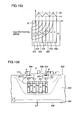
- Fig. 148 is a cross sectional view schematically showing the first configuration of a semiconductor device according to a prior art and shows a configuration that corresponds to a case where a MOS-FET is posited as a concrete active element structure.
- an n- epitaxial layer 102 is formed on the first main surface side of an n + drain region 101 of the MOS-FET.
- a pn-repeating structure wherein n-type drift regions 103 and p-type impurity regions 104 are repeated in alternation is formed within this n - epitaxial layer 102.
- n-type impurity concentration of n-type drift region 103 and the p-type impurity concentration of p-type impurity region 104 in each pair are set at substantially the same level.
- a p-type body region 105 is formed on the first main surface side of p-type impurity region 104. This p-type body region 105 is also located on, at least, a portion of n-type drift region 103 on the first main surface side so as to form a main pn junction with n-type drift region 103.
- An n + source region 106 of a MOS-FET and a p + contact region 107 for making a low resistance contact with p-type body region 105 are formed side by side in the first main surface within this p-type body region 105.
- a gate electrode 109 is formed above the first main surface so as to face p-type body region 105 located between n-type drift region 103 and n + source region 106 via a gate insulating film 108.
- p-type body region 105 which faces gate electrode 109, is inverted to an n-type so that a channel region is formed.
- a drain metal wire 111 is formed on the second main surface so as to contact n + drain region 101.
- the source electrode part is electrically connected to n + source region 106 and p + contact region 107 through a contact hole provided in an interlayer insulating film on the first main surface and via a barrier metal.
- this portion is not important and, therefore, the source electrode part is simplified and expressed using solid lines throughout all of the drawings.
- n + drain region 101 is several times to several tens of times thicker than the effective element portion in the actual element, n + drain region 101 is expressed as thinner than the effective element portion in the drawings for the purpose of simplification.
- scales, ratios of dimensions, and the like are deformed in order to simphfy the expression and, therefore, the respective dimensions in the drawings are not necessarily precise.
- n-type drift regions 103 and p-type impurity regions 104 respectively, have substantially the same impurity concentration in the center portion and edge portions of the pn-repeating structure.
- Fig. 149 is a cross sectional view schematically showing the second configuration of the semiconductor device according to the prior art.
- an n - epitaxial layer 102 has a buried multi-layer epitaxial structure and a p-type impurity region 104 is formed of a plurality of p-type regions 104a that are integrated in the depth direction of the semiconductor substrate in this configuration.
- p-type impurity regions 104 respectively, have the same impurity concentration in the center portion and edge portions of the pn-repeating structure.
- each p-type impurity region 104 is an intrinsic structure and this is a concentration distribution due to the manufacturing method, which has no bearing on the concentration gradient in the part in the lateral direction discussed in the present invention.
- concentration gradient in the upward and downward directions is depicted in only two stages for the purpose of simplification, in practice this concentration sequentially changes.
- a manufacturing method according to this prior art is characterized in that n- epitaxial layer 102, having a comparatively high concentration to the extent that the concentration thereof is balanced with that of the p-type layers, is used for the purpose of simplifying the process of formation of the buried layers.
- a heat treatment is carried out after forming p-type buried diffusion layers 104a within n- epitaxial layer 102 in such a manner and, therefore, p-type impurity region 104 becomes of a form well-known in Japan as "round sweet balls of confectionary on a skewer.”
- Fig. 150 is a cross sectional view schematically showing the third configuration of the semiconductor device according to the prior art.
- n-type drift regions 103 and p-type impurity regions 104 form pairs and a trench 123 filled in with a filling 124 is arranged between the members of each combined pn pair in this configuration.
- Fig. 151 shows the appearance of electrical field concentration in the structure corresponding to this Fig. 150.
- the dark portion in this figure indicates a portion of high electrical field concentration and it is seen that an electrical field concentrates on portions (regions shown by arrows) wherein the pn-repeating structure ends.
- an FP (Field Plate) structure is adopted for the termination structure portions instead of the multiple guard ring called an FLR (Field Limiting Ring) or an FFR (Floating Field Ring).
- Prior Art 1 has been announced as a method for preventing the loss of the high withstand voltage of the main cell portion by setting a specific concentration of the p-type layers and of the n-type layers outside of the portions wherein the pn-repeating structures ends. According to this technique, however, there is a problem wherein implementation is difficult due to the reasons described below.
- This Prior Art 1 shows improvement of the termination structure itself in the pn-repeating structure.
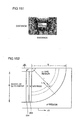
- Fig. 152 the structure shown in Fig. 152 is shown in the above described Prior Art 1.
- a region of which the effective conductive type and concentration can be regarded as those of a low concentration p- region in a fan form of a quarter of a circle having a radius of R of the thickness (depth) of an n layer is formed from a portion wherein the repetition of p layers 204 and n layers 203 ends.
- a p - region cannot actually be formed to have such a concentration distribution. Therefore, it is necessary for the concentration distribution of the effective p - region to have an attenuation curve as shown in Fig. 153.
- the only requirements at this time are a form wherein the equipotential surfaces are aligned in fans at equal intervals as shown in Fig. 155 and a zigzag electrical field intensity distribution that is exposed to the surface wherein the peaks and the troughs have the same height and depth, respectively.
- each of the concentrations of p i regions 204 and n i regions 203 are posited as being uniform within the single diffusion layer in the upward, downward, leftward and rightward directions.
- this Prior Art 1 discloses the design of the entirety of the element in a form that includes the termination structure by literally extending the super junction structure of the repeating cell portions to the termination structure portions in some manner according to SJT, that is to say, "Super Junction Termination structure,” wherein a repeating cell portion in the center and a termination structure have a one-to-one correspondence so as to be indivisible having a very limitative structure while "manner of connection" of a repeating cell portion to a general termination structure portion is described in the present invention, which is essentially different from the above.
- the electrical field distribution closest to the surface becomes of a zigzag form and, in the case that the peaks and troughs all have the same value, the maximum withstand voltage can be obtained. Therefore, in the case that the all of the concentrations of n and p regions 203 and 204 are made uniform so that the equipotential surfaces (lines) distribute in fan forms at equal intervals, as shown in Fig. 155, it is necessary to carry out an adjustment of the width of each of the regions 203 and 204.
- SJT is considered to be impractical because it has the following two problems.
- concentration regulation for forming an SJT structure is too complicated and it is necessary to apply an interval design that agrees with the concentration arrangement of the repeating cell portions that are different from the termination structure portions to the SJT part after examining the arrangement in detail before carrying out the actual design and, in addition, it is physically and mechanically difficult to fabricate a semiconductor chip structure to include terminal edges.
- the present invention has the advantage that both design and manufacturing method are simple because the relative concentrations in the vicinity of the terminal edges of the repeating cell portions may be adjusted using comparatively simple arithmetic.
- an SJT structure can only be implemented in the case of manufacture by means of a buried multi-layer epitaxial growth method and lacks versatility in that it cannot be actually manufactured in the case wherein a trench sidewall diffusion is used.
- a vertical-type MOS-FET has inside region 301 that is doped so as to be a low level n-type.
- a base region 303 of the opposite conductive type (p) is provided in the upper side surface 302 of the semiconductor substrate.
- a source region 304 of the first conductive type (n) is buried within base region 303.
- a gate electrode 308 is arranged above surface 302 so as to be insulated from the surface.
- a drain region 307 that is highly doped so as to be of the same conductive type as inside region 301 is provided in the surface 306 on the opposite side.
- Auxiliary semiconductor regions 311 and 312 are arranged in a range of the space-charge region that spreads at the time of reverse voltage application within the inside region 301. At least two regions 211 of a conductive type opposite to that of the inside region are provided. Auxiliary regions 312 having the same the same conductive type (n) as inside region 301 and being more highly doped than the inside region arranged between regions 311. The auxiliary regions are surrounded from all directions by a single region. This single region is of the same conductive type as the inside region, as well as regions 312, and is more highly doped than the inside region.
- n- region 301 which has a low concentration
- the impurity concentration of this outer peripheral portion is not specifically described and only the method of formation of a cell portion is discussed.
- the impurity concentration of a portion wherein a pn-repeating structure is not formed in this Prior Art 2 is presumed to be set at the impurity concentration that is reverse calculated from a value obtained by adding a manufacturing margin to the element withstand voltage set for the power MOS-FET of a conventional structure (structure that does not have pn repetition).
- a manufacturing margin to the element withstand voltage set for the power MOS-FET of a conventional structure (structure that does not have pn repetition).
- An object of the present invention is to provide a structure which improves the trade-off relationship between the main withstanding voltage and the ON resistance, and a manufacturing method capable of implementing such a structure in a semiconductor device based on a three-dimensional multiple RESURF effect.
- a semiconductor device of the present invention is a semiconductor device having a repeating structure, wherein a structure where a first impurity region of a first conductive type and a second impurity region of a second conductive type are aligned side by side, is repeated twice or more in a semiconductor substrate of the first conductive type, characterized in that a low concentration region, which is either the first or the second impurity region located at the outermost portion in the repeating structure, has the lowest impurity concentration or has the least generally effective charge amount from among all of the first and second impurity regions forming the repeating structure.
- a portion of the concentration of the outermost portion in the repeating structure is converted to have a concentration lower than the center portion and, thereby, the "mitigating region” that gradually mitigates the strong "three-dimensional multiple RESURF effect” used in the repeating cell portion in the center portion is provided so that the connection with a conventional so-called “termination structure” portion formed of a guard ring or a field plate is made easier and the main withstanding voltage drop caused by "mismatch" in the connection between the strong "three-dimensional multiple RESURF effect” portion and a so-called “termination structure” portion can be restricted.
- the impurity concentration of the low concentration region is preferably no lower than 30% and no higher than 70% of the impurity concentration of the high concentration region that is either the first or second impurity region located closer to the center portion of the repeating structure than is the low concentration region.
- the impurity concentration of the middle concentration region which is of the above described first or second impurity region located between the low concentration region and the high concentration region, is higher than the impurity concentration of the low concentration region and is lower than the impurity concentration of the high concentration region.
- the semiconductor substrate preferably has a first main surface and a second main surface facing each other wherein a third impurity region of the second conductive type is formed in, at least, a portion of at least one of the plurality of the first impurity regions on the first main surface side that forms the repeating structure so as to form a main pn junctions with the first impurity regions and a fourth impurity region of the first conductive type is formed on the second main surface side of the repeating structure.
- the present invention can be applied to an element having a vertical-type structure.
- the third impurity region that forms the main pn junctions with the first impurity regions is preferably a body region of an insulating gate-type field effect transistor portion.
- the present invention can be applied to an element having a MOS-FET.
- the low concentration regions located at the outermost portion in the repeating structure do not form active elements.
- the withstand voltage alone can be maintained in the low concentration regions having a concentration gradient that tends to be unstable at the time of switching operation without forming an element, such as a MOS-FET, so that stable switching operation can be obtained.
- a third impurity region of the second conductive type formed in, at least, a portion of the upper portion of the first impurity region close to an end that extends in one specific direction
- a fourth impurity region of the first conductive type formed in, at least, a portion of the upper portion of the first impurity region close to an end in the direction opposite to the above described one specific direction
- a first electrode electrically connected to the third impurity region and a second electrode electrically connected to a fourth impurity region are further provided, wherein the first and second electrodes are both formed on the first main surface.
- the present invention can be applied to an element having a lateral-type structure.
- the semiconductor substrate preferably has a first main surface and a second main surface that face each other and has a plurality of trenches in the first main surface, wherein the repeating structure has a structure where a structure in which the first and second impurity regions,are arranged side by side with a trench located in between is repeated twice or more.
- the present invention can be applied to an element having a trench, for example, an ST (Super Trench) type element.
- an ST Super Trench
- the impurity concentration of the low concentration region is preferably no lower than 30% and no higher than 70% of the impurity concentration of the high concentration region, which is the first or second impurity region, that is located closer to the center portion of the repeating structure than is the low concentration region.
- the impurity concentration of the middle concentration region which is either the first or the second impurity region, located between the low concentration region and the high concentration region is preferably higher than the impurity concentration of the low concentration region and lower than the impurity concentration of the high concentration region.
- the middle concentration region in an element having a trench in the above described manner, it becomes possible to continuously change the concentration gradient from the center portion of the pn-repeating structure to the first conductive type region of the semiconductor substrate.
- a first impurity region is formed on one side of a mesa portion of a semiconductor device surrounded by a plurality of trenches and a second impurity region is formed in the surface of the other side and a third impurity region of the second conductive type is formed in, at least, a portion of the above described first main surface side of the first impurity region so that the first impurity region and the main pn junction are formed.
- the present invention can be applied to an element having an ST-type mesa region.
- the third impurity region forming a pn junction primarily with the first impurity region is a body region of an insulating gate-type field effect transistor portion.
- the present invention can be applied to an ST-type element having a MOS-FET, that is to say, to an STM (Super Trench power MOS-FET).
- the low concentration region located at the outermost portion of the repeating structure preferably does not form a passive element.
- withstand voltage alone can be maintained in the ST-type element without forming an element, such as a MOS-FET, in a low concentration region having a concentration gradient which easily becomes unstable at the time of switching operation so that a stable switching operation can be obtained.
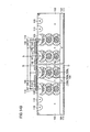
- the trench positioned at the outermost part of the plurality of trenches is a first trench in a dotted line form having a surface pattern in a dotted line form wherein a plurality of first holes are arranged at intervals in a predetermined direction in the first main surface and the low concentration region is formed so as to be located along one of the sidewalls of the first trench of a dotted line form.
- the present invention can be applied to an element having a trench in a dotted line form, that is to say, to an element having a DLT (Dotted Line Trench) so that the manufacturing process can be simplified.
- DLT Dotted Line Trench
- the total of the length of the sidewalls on one side of the first main surface of a plurality of first holes forming the first trench of a dotted line form is preferably no lower than 30% and no more than 70% of the length of the sidewalls on one side in the first main surface of the trench continuously extending along a location closer to the center portion than the first trench of a dotted line form.
- the length and the intervals of the holes of the trench of the dotted line form are adjusted and, thereby, the impurity concentration of the low concentration region can be adjusted.
- the concentration gradient from the center portion of the pn-repeating structure to the first conductive type region of the semiconductor substrate is in a range that can be regarded as continuous.
- the trench located between the first trench of a dotted line form and the continuously extending trench is preferably a second trench of a dotted line form having a surface pattern in a dotted line form wherein a plurality of second holes are arranged at intervals in a predetermined direction in the first main surface and the sum of length of the sidewalls on one side in the first main surface of the plurality of second holes that form the second trench of a dotted line form is greater than the sum of length of the sidewalls on one side in the first main surface of the plurality of first holes that form the first trench of a dotted line form and is less than the length of the sidewall on one side in the first main surface of the continuously extending trench in the location closer to the center portion than the second trench of a dotted line form.
- the trenches of dotted line forms are provided in a step-by-step manner in the element having the DLT structure and, thereby, the concentration gradient can be regarded as being continuous from the center portion of the pn-repeating structure to the first conductive type region of the semiconductor substrate.
- the first impurity region is preferably formed on one of the sides of the mesa portion of the semiconductor device surrounded by a plurality of trenches and the second impurity region is formed on the other of the sides and the third impurity region of the second conductive type is formed in, at least, a portion on the first main surface side of the first impurity region so as to form a main pn junction with the first impurity region.
- the present invention can be applied to an element having a DLT structure and having an ST-type mesa region.
- the third impurity region which forms the main pn junction with the first impurity region, is a body region of an insulating gate-type field effect transistor portion
- the present invention can be applied to an element having a MOS-FET in an ST-type type element having a DLT structure, that is to say, to an STM (Super Trench power MOS-FET).
- STM Super Trench power MOS-FET
- the low concentration region located at the outermost portion of the repeating structure preferably does not form an active element.
- the withstand voltage alone can be maintained without forming an element, such as a MOS-FET, in the low concentration region having a concentration gradient that tends to become unstable at the time of switching operation in an ST-type element having a DLT structure so that a stable switching operation can be obtained.
- an element such as a MOS-FET
- the semiconductor substrate preferably has a first main surface and a second main surface facing each other and has a plurality of trenches including first and second trenches adjoining each other in the first main surface wherein a structure where a first impurity region is formed in each of the two sidewalls of the first trench and a second impurity region is formed in each of the two sidewalls of the second trench is repeated twice or more.
- the present invention can be applied to an element having a twin trench structure.
- the impurity concentration of the low concentration region is no lower than 30% and no higher than 70% of the impurity concentration of the high concentration region that is either the first or second impurity region located closer to the center portion in the repeating structure than the low concentration region.
- the impurity concentration of the middle concentration region which is either the first or second impurity region, located between the low concentration region and the high concentration region is preferably higher than the impurity concentration of the low concentration region and is lower than the impurity concentration of the high concentration region.
- trenches of dotted line forms are provided in a side by side manner in an element having a twin trench structure and, thereby, the concentration gradient from the center portion of the pn-repeating structure to the first conductive type region of the semiconductor substrate can be regarded as being continuous.
- a first impurity region is preferably formed on one side of the mesa portion of the semiconductor substrate surrounded by a plurality of trenches, a second impurity region is formed on the other side and a third impurity region of the second conductive type is formed on, at least, a portion of the first main surface side of the first impurity region so as to form a main pn junction with the first impurity region.
- the present invention can be applied to an element having twin trench structure.
- the third impurity region forming the main pn junction with the first impurity region is preferably a body region of an insulating gate-type field effect transistor portion.
- the present invention can be applied to an element having a MOS-FET in an element having a twin trench structure.
- the low concentration region located at the outermost portion of the repeating structure preferably does not form an active element.
- withstand voltage alone can be maintained without forming an element, such as a MOS-FET; in the low concentration region having a concentration gradient that tends to become unstable at the time of switching operation in an element having a twin trench structure so that a stable switching operation can be obtained.
- the trench located at the outermost portion of the plurality of trenches is the first trench of a dotted line form having a surface pattern of a dotted line form wherein a plurality of first holes are arranged at intervals in a predetermined direction in the first main surface and the low concentration region is formed so as to be located on one of the sidewalls of the first trench of a dotted line form.
- the present invention can be applied to an element having a twin trench structure and having a DLT structure so that the manufacturing process can be simplified.
- the sum of the lengths of the sidewalls on one side in the first main surface of the plurality of first holes forming the first trench of a dotted line form is no greater than 30% and no less than 70% of the length of the sidewall on one side in the first main surface of the trench that extends continuously in a location closer to the center portion than the first trench of a dotted line form.
- the impurity concentration of the low concentration region can be adjusted.
- the concentration gradient from the center portion of the pn-repeating structure to the first conductive region of the semiconductor device to be in a range that is regarded as being continuous.
- a trench located between the first trench of a dotted line form and the continuously extending trench is a second trench of a dotted line form having a surface pattern of a dotted line form wherein a plurality of second holes are arranged at intervals in a predetermined direction in the first main surface and the sum of the lengths of the sidewalls on one side of the plurality of second holes forming the second trench of a dotted line form in the first main surface is greater than the sum of the lengths of the sidewalls on one side of the plurality of first holes forming the first trench of a dotted line form and is smaller than the length of the sidewall on one side of the continuously extending trench that is closer to the center portion than the second trench of a dotted line form in the above described first main surface.
- the concentration gradient from the center portion of the pn-repeating structure to the first conductive type region of the semiconductor substrate can be regarded as being continuous.
- a first impurity region is preferably formed on one side of the mesa portion of the semiconductor substrate surrounded by the plurality of trenches, a second impurity region is formed on the opposite side of the mesa portion and a third impurity region of the second conductive type is formed in, at least, a portion on the above described first main surface side of the first impurity region so as to form a main pn junction with the first impurity region.
- the present invention has a twin trench structure and a DLT structure and can be applied to an element having an ST-type mesa region.
- the third impurity region forming a main pn junction with the first impurity region is preferably a body region of an insulating gate-type field effect transistor portion.
- the present invention can be applied to an element having a MOS-FET in an element having a twin trench structure and a DLT structure.
- the low concentration region located at the outermost portion of the repeating structure preferably does not form an active element.
- the withstand voltage alone can be maintained without forming an element, such as a MOS-FET, in the low concentration region having a concentration gradient that tends to become unstable at the time of switching operation in an ST-type element having a twin trench structure and a DLT structure so that a stable switching operation can be obtained.
- an element such as a MOS-FET
- a manufacturing method for a semiconductor device of the present invention is characterized in that the low concentration region and other first and second impurity regions are formed by independently changing the concentration so that the low concentration region, which is either the first or second impurity region located at the outermost portion of the repeating structure, has the lowest impurity concentration or has the least generally effective charge amount from among all of the first and second impurity regions forming the repeating structure in a manufacturing method for a semiconductor device having a repeating structure wherein a structure where a first impurity region of a first conductive type and a second impurity region of a second conductive type are aligned side by side is repeated twice, or more, in a semiconductor substrate of the first conductive type
- the outermost portion of the repeating structure has a concentration lower than that of the center portion and, thereby, the concentration of i layer of a pin diode formed of the repeating structure and the region of the first conductive type of the semiconductor substrate can be lowered.
- concentration of the i layer so that the withstand voltage obtained at the outermost portion of the repeating structure becomes greater than the withstand voltage obtained in the center portion. Therefore, an increase in the withstand voltage at a cell portion can be achieved, in contrast to the prior art.
- the low concentration region and other first and second impurity regions are preferably formed by means of ion implantation and heat treatment in order to independently control the concentration so as to form the low concentration region and other first and second impurity regions of which the concentrations have been independently changed.
- this method is suitable for a manufacturing method for a low withstand voltage element.
- the low concentration region and other first and second impurity regions are preferably formed by means of ion implantation and multi-stage epitaxial growth in order to independently control the concentration so as to form the low concentration region and other first and second impurity regions of which the concentrations have been independently changed.
- epitaxial layers can, in principle, be layered infinitely. Accordingly, this method is suitable for a manufacturing method for high withstand voltage element.
- the low concentration region and other first and second impurity regions are favorably formed by independently changing the concentrations and, therefore, the above described low concentration region and other first and second impurity regions have independently changed concentrations and are formed by means of ion implantation wherein implantation energy is changed according to multi-stages.
- this method is suitable for a manufacturing method for a low withstand voltage element.
- impurity ions injected from the first openings in a mask for ion implantation preferably form the first and second impurity regions, other than the low concentration region, while impurity ions injected from the second openings, of which the total area of the openings is smaller than that of the first openings, form the low concentration region in order to independently change the concentrations at the time of the formation of the low concentration region and other first and second impurity regions.
- openings of which the areas of the openings differ, are used and, thereby, high concentration regions are low concentration regions can be formed at the same time through a single ion implantation process so that simplification of the process can be achieved.
- the second openings preferably have a configuration wherein a plurality of microscopic openings separated from each other are densely arranged so that impurity ions injected from each of the plurality of microscopic openings are integrated by applying a heat treatment so as to form a finished low concentration region of which the average impurity concentration is lower than that of the other first and second impurity regions.
- the openings, of which the areas of the openings differ can easily be formed.
- the above described manufacturing method for a semiconductor device preferably is further provided with the step of creating one, or more, trenches and a trench of a dotted line form having a surface pattern of a dotted line form in the first main surface at the same time by arranging the trench of a dotted line form so as to be located along the outside of the above one, or more, trenches wherein a plurality of first holes are arranged at intervals in a predetermined direction and the step of forming a low concentration region on the one sidewall of the trench of a dotted line form and the other first and second impurity regions on one of the sidewalls of the above one, or more, trenches at the same time by simultaneously implanting ions in the above one, or more, trenches and in one of sidewalls of respective trenches of a dotted line form.
- the trenches of a dotted line form are used in the STM structure and, thereby, a high concentration region and a low concentration region can be simultaneously formed by means of a single ion implantation step so that simplification of the process can be achieved.
- the above described manufacturing method for a semiconductor device preferably is further provided with the step of creating two, or more, trenches in the first main surface of the semiconductor substrate, the step of implantation of impurities in order to form the first and second impurity regions and the step of forming a low concentration region by substantially lowering the concentration of the impurities that have already been implanted through the ion implantation of impurities of a conductive type opposite to the already implanted impurities in the one sidewall of the trench located at the outermost portion.
- the concentration of the impurity region at the outermost portion in the repeating structure can be lowered by means of counter doping.
- the above described manufacturing method for a semiconductor device preferably is further provided with the step of creating one, or more, trenches in the first main surface of the semiconductor substrate, the step of ion implantation with a first implantation amount in order to form first or second impurity regions on one side of the respective sidewalls of the above one, or more, trenches, the step of creating a new trench at the outermost portion outside of the above one, or more, trenches in the condition wherein each of the above one, or more, trenches is filled in with a filling layer and the step of ion implantation with a second implantation amount smaller than the first implantation amount in order to form a low concentration region on one sidewall of the trench at the outermost portion.
- the trenches in the center portion and at the outermost portion in the pn-repeating structure can be separately created and ion implantations can be separately implemented in the STM structure.
- the above described manufacturing method for a semiconductor device preferably is further provided with the step of simultaneously creating two, or more, trenches including first and second trenches adjoining each other in the first main surface of the semiconductor substrate and a trench of a dotted line form that is located along the outside of the two, or more, trenches wherein the plurality of first holes are arranged at intervals in a predetermined direction and that, thereby, has a surface pattern of a dotted line form in the first main surface, the step of ion implantation of the first impurities in order to form the first impurity region in each of the two sidewalls of the first trench and the step of ion implantation of the second impurities in order to form the second impurity region in each of the two sidewalls of the second trench, wherein the low concentration region is formed on both sidewalls of the trench of a dotted line form by means of an implantation at the same time as the ion implantation of the first or second impurities.
- a trench of a dotted line form is used in a twin trench structure and, thereby, a high concentration region and a low concentration region can be simultaneously formed by means of a single ion implantation step so that simplification of the process can be achieved.
- the above described manufacturing method for a semiconductor device preferably is further provided with the step of creating a first group of trenches made of a plurality of first trenches in the first main surface of the semiconductor substrate, the step of ion implantation for forming the first impurity regions in the sidewalls on both sides of each of the first trenches, the step of creating a second group of trenches made of a plurality of second trenches in the first main surface so that the first trenches and the second trenches are located in an alternating manner, the step of ion implantation for forming the second impurity regions in the sidewalls on both sides of each of the second trenches and the step of the implantation of impurities of a conductive type opposite to that of the already implanted impurities into the sidewalls on both sides of the above described trench positioned at the outermost portion under the condition wherein the first and second trenches arranged in an alternating manner, except the trench located at the outermost portion, are filled in with a filling layer so
- the concentration of the impurities at the outermost portion of the repeating structure can be lowered by means of counter doping.
- the above described manufacturing method for a semiconductor device is preferably provided with the step of creating a first trench group made of a plurality of first trenches in the first main surface of the above described semiconductor substrate, the step of ion implantation for forming the first impurity regions in the sidewalls on both sides of each of the first trenches, the step of creating a second group of trenches made of a plurality of second trenches in the first main surface under the condition wherein each of the first trenches is filled in with a filling layer so that the first trenches and the second trenches are located in an alternating manner, the step of ion implantation for forming the second impurity regions in the sidewalls on both sides of each of the second trenches, the step of creating a new trench at the outermost portion outside of the trench located at the outermost portion of the first and second trenches arranged in an alternating manner under the condition wherein each of the first and second trenches is filled in with a filling layer and the step of forming a
- the trenches of the center portion and of the outermost portion in the repeating structure can be separately fabricated and ion implantations can also be separately carried out.
- the above described manufacturing method for a semiconductor device preferably is further provided with the step of simultaneously creating a first group of trenches made of a plurality of first trenches and a second group of trenches made of a plurality of second trenches in the first main surface of the semiconductor substrate so that the first trenches and the second trenches are located in an alternating manner, the step of ion implantation for forming the first impurity regions in the sidewalls on both sides of each of the plurality of first trenches forming the first group of trenches under the condition wherein the second group of trenches is filled in with a first filling layer, the step of ion implantation for forming the second impurity regions in the sidewalls on both sides of each of the plurality of second trenches forming the second group of trenches under the condition wherein the first group of trenches is filled in with a second filling layer and the step of implanting impurity ions of a conductive type opposite to the already implanted impurities into the
- the concentration of the impurity region of the outermost portion in the repeating structure can be lowered by means of counter doping.
- the above described manufacturing method for a semiconductor device is preferably provided with the step of simultaneously creating a first group of trenches made of a plurality of first trenches and a second group of trenches made of a plurality of second trenches in the first main surface to semiconductor substrate so that the first trenches and the second trenches are located in an alternating manner, the step of ion implantation for forming the first impurity regions in the sidewalls on both sides of each of the plurality of first trenches forming the first group of trenches under the condition wherein the second group of trenches is filled in with a first filling layer and the step of ion implantation for forming the second impurity regions in the sidewalls on both sides of each of the plurality of second trenches forming the second group of trenches under the condition wherein the first group of trenches is filled in with a second filling layer, wherein the trench at the outermost portion, located at the outermost portion, from among the trenches of the plurality of first trench
- a high concentration region and a low concentration region can be simultaneously formed through a single ion implantation step by using a trench of a dotted line form and, thereby, simplification of the process can be achieved.
- the above described manufacturing method for a semiconductor device is preferably provided with the step of forming two, or more, trenches in the first main surface of the semiconductor substrate, the step of ion implantation of impurities for forming the first or second impurity regions in the sidewalls on one side of the two, or more, trenches and the step of ion implantation of impurities of the same conductive type as that of the already implanted impurities into the sidewalls on one side of the trenches, other than the trench located at the outermost portion, under the condition wherein the trench located at the outermost portion, from among the two, or more, trenches, is filled in with a filling layer so as to substantially increase the concentration of the already implanted impurities and, thereby, the above described first or second impurity regions in the sidewalls of the trench located at the outermost portion becomes a region of a comparatively low concentration.
- ion implantation of impurities of the same conductive type is again carried out in the sidewalls of the trenches of the center portion and, thereby, the impurity concentration of the center portion is enhanced so that the concentration of the impurity regions at the outermost portion of the repeating structure can be made to be of a comparatively low concentration.
- the above described manufacturing method for a semiconductor device is preferably further provided with the step of creating a first group of trenches made of a plurality of first trenches in the first main surface of the semiconductor substrate, the step of ion implantation for forming the first impurity regions in the sidewalls on both sides of each of the first trenches, the step of forming a second group of trenches made of a plurality of second trenches in first main surface so that the first trenches and the second trenches are located in an alternating manner, the step of ion implantation for forming the second impurity regions in the sidewalls on both sides of each of the second trenches and the step of implanting impurities of the same conductive type as the already implanted impurities in the sidewalls on both sides of the trenches, other than the trench located at the outermost portion, under the condition wherein the trench located at the outermost portion, from among the first and second trenches arranged in an alternating manner is filled in with a filling layer so
- the twin trench structure ion implantation of impurities of the same conductive type is again carried out in the sidewalls of the center portion and, thereby, the impurity concentration of the center portion is enhanced so that the concentration of the impurity region at the outermost portion of the repeating structure can be lowered to have a comparatively low concentration.
- the above described manufacturing method for a semiconductor device preferably is further provided with the step of simultaneously creating a first group of trenches made of a plurality of first trenches and a second group of trenches made of a plurality of second trenches in the first main surface of the semiconductor substrate so that the first trenches and second trenches are located in an alternating manner, the step of ion implantation for forming the first impurity regions in the sidewalls on both sides of each of the plurality of first trenches forming the first group of trenches under the condition wherein the second group of trenches is filled in with a first filling layer, the step of ion implantation for forming the second impurity regions in the sidewalls on both sides of each of the plurality of second trenches forming the second group of trenches under the condition wherein the first group of trenches is filled in with a second filling layer and the step of implanting impurity ions of the same conductive type as that of the already implanted impurities in the
- ion implantation of impurities of the same conductive type is again carried out in the sidewalls of the trenches in the center portion and, thereby, the impurity concentration of the center portion is enhanced so that the impurity region at the outermost portion of the repeating structure can be made to have a comparatively low concentration.
- portions to which the same alphanumeric, or other, symbols are attached indicate the same regions or regions having the same operation or function and a portion to which the same number with an alphanumeric subscript is attached indicates a portion having a similar operation or function to a region having the same number without the alphanumeric subscript.
- the impurity concentration of the impurity region located at the outermost portion of the pn-repeating structure of an n-type impurity region 3 and a p-type impurity region 4 is set at a low concentration to the extent that the structure can generally be regarded as a pin diode structure.
- the impurity concentration of the impurity region located at the outermost portion of the pn-repeating structure has the lowest impurity concentration from among all of the impurity regions forming the pn-repeating structure.
- the impurity concentration of n - epitaxial layer 2 is generally set at a concentration that is lower, by approximately one order, than a conventional element having the same grade of main withstanding voltage.
- a pin diode can be formed so that an approximately trapezoidal electrical field intensity distribution form can be obtained, in contrast to the case of a p + /n - junction alone having a triangular electrical field intensity distribution. Therefore, the thickness of n - epitaxial layer 2 can be made to be approximately half of that of a conventional element having the same grade of main withstanding voltage.
- the withstand voltage of the cell portion differs from that of the case of a conventional MOS-FET structure and has a value obtained by the multiplication of a ⁇ 2 ⁇ 10 5 V/cm by the thickness of n-epitaxial layer 1.
- the constant a is a number that is experimentally found and is a number of from approximately 0.6 to 1.2.
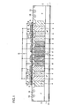
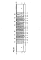
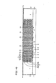
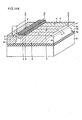
- Fig. 1 shows a configuration that corresponds to the case wherein a MOS-FET is posited as a concrete active element structure.
- an n - epitaxial layer 2 is formed on the first main surface side of an n + drain region 1 of the MOS-FET.
- a pn-repeating structure is formed within this n- epitaxial layer 2 wherein n-type drift regions 3 and p-type impurity regions 4 are repeated in alternation.
- the vicinity of the center of the element having this pn-repeating structure is omitted for simplification of explanation and the pitch of pn repetition is approximately 1 ⁇ m to 20 ⁇ m and, therefore, several hundreds to several tens of thousands of pairs of n-type drift regions 3 and p-type impurity regions 4 usually exist in the form of repeated combinations in this portion.
- the n-type impurity concentration of an n-type drift region 3 and the p-type impurity concentration of a p-type impurity region 4, which are combined in a pair, are set at substantially the same level.
- a p-type body region 5 is formed on the first main surface side of a p-type impurity region 4. This p-type body region 5 is located in, at least, a portion of an n-type drift region 3 on the first main surface side so as to form a main pn junction with n-type drift region 3.
- An n + source region 6 of a MOS-FET and a p + contact region 7 for making a low resistance contact with this p-type body region 5 are formed side by side in the first main surface within this p-type body region 5.
- a gate electrode 9 is formed above the first main surface so as to face p-type body region 5 located between n-type drift region 3 and n + source region 6 via a gate insulating film 8.
- a positive voltage is applied to this gate electrode 9, p-type body region 5 facing gate electrode 9 is inverted to an n-type so that a channel region is formed.
- Gate insulating film 8 is made of, for example, a silicon oxide film and gate electrode 9 is made of, for example, a polycrystal silicon into which a high concentration of impurities is introduced.
- a source electrode 10 made of a material including, for example, aluminum (Al) is formed on the first main surface so as to be electrically connected to n + source region 6 and p + contact region 7.
- a drain metal wire 11 is formed on the second main surface so as to contact n + drain region 1.
- a source electrode part is electrically connected to an n + source region 6 and to a p + contact region 7 through a contact hole provided in the interlayer insulating film above the first main surface and via a barrier metal.
- this part is not important and, therefore, the source electrode part is simplified and is expressed using a solid line throughout the drawings.
- n + drain region 1 is several times to several tens of times thicker than the thickness of the effective element portion
- n + drain region 1 is expressed as being thinner than the effective element portion in the drawings for the purpose of simplification.
- scales, ratios of dimensions, and the like are deformed in order to simplify the expression and, therefore, the respective dimensions in the drawings are not necessarily precise.
- a multiple guard ring structure made of p-type impurity regions 15 is provided as a termination structure of the pn-repeating structure
- the structure of this portion is not particularly limited in the present invention and this guard ring structure may be replaced with another termination structure.
- termination structures of the other embodiments described below can also be replaced in the same manner as in the above.
- the structure of the present embodiment is characterized by the setting of the impurity concentration in the pn-repeating structure of n-type drift regions 3 and p-type impurity regions 4.
- a pair made up of n-type impurity region 3 and p-type impurity region 4 located at the outermost portion, which is the termination portion of this pn-repeating structure, has the lowest impurity concentration (or the least general effective charge amount) from among all of the n-type impurity regions 3 and p-type impurity regions 4 forming the pn-repeating structure.
- n-type drift region 3 may be located at the outermost portions on both sides, left and right, of the pn-repeating structure.
- a p-type impurity region 4 may be located at one outermost portion of the pn-repeating structure and n-type drift region 3 is located at the other outermost portion.
- the pn-repeating structure has a concentration change of three stages (or change in general effective charge amount) in the present embodiment.
- n-type drift regions 3 and p-type impurity regions 4 in the center portion are a high concentration region, one pair made up of n-type drift region 3 and p-type impurity region 4 at the outermost portion is a low concentration region and one pair made up of n-type drift region 3 and p-type impurity region 4 located between the center portion and the outermost portion is a middle concentration region.
- the difference in these impurity concentrations is distinguished by the hatching in the drawings of the present specification. That is to say, the denser is the hatching, the higher is the concentration (or the greater is the general effective charge amount) and the less dense is the hatching, the lower is the concentration (or the smaller is the general effective charge amount) in the pn-repeating structure.
- regions without hatching are also illustrated and indicate regions of the lowest impurity concentration (or the smallest general effective charge amount) in the pn-repeating structure.
- the impurity concentration (or general effective charge amount) of high concentration regions 3 and 4 is posited as 100%
- the impurity concentration (or general effective charge amount) of middle concentration regions 3 and 4 is set at 67% and the impurity concentration (or general effective charge amount) of the low concentration regions 3 and 4 is set at 33% at the time of division into three.
- the respective concentrations (or general effective charge amount) are allowed to have ranges and the impurity concentration (or general effective charge amount) of the middle concentration regions 3 and 4 may be approximately 60% to 80% while the impurity concentration (or general effective charge amount) of the low concentration regions 3 and 4 may be approximately 20% to 45%.
- n-type drift region 3 and p-type impurity region 4 at the outermost portion of the pn-repeating structure have the lowest impurity concentration (or smallest general effective charge amount) from among all of the n-type drift regions 3 and p-type impurity regions 4 forming the pn-repeating structure.
- a buffer region of middle concentration between the pin diode structure, which is in many cases formed at the outermost portion of the pn-repeating structure, and the repeating cell portion is formed so that the difference in the formation of the electrical field distribution occurring in the respective regions is eased and, therefore, the reduction of the main withstanding voltage in the connection portion can be restricted to a great extent in comparison with the case wherein the repeating cell portion and the conventional termination structure portion are directly connected.
- the gist of Prior Art 1 indicates a guiding principle of a method for designing the entirety of an element in a form that includes the termination structure by somehow extending the super junction structure of the repeating cell portion to the termination structure portion.
- the gist of the present invention is "a structure, and manufacturing method for the same, wherein a buffer region of the electrical field between the insides of the cells of a high impurity concentration and the termination portion of a low impurity concentration at the time when a portion similar to the super junction effect described in Prior Art 1 wherein a three dimensional multiple RESURF effect is used and the termination structure portion having an electrical field distribution of a flat trapezoidal form such as of a pin diode having the conventional structure.” Therefore, though Prior Art 1 and the present invention share the same purpose and effect that a high withstand voltage implemented in the same portion is not lost at the termination portion, they are formed from totally different points of view.
- Prior Art 1 is a structure that includes a detailed regulation of the structure of the surface portion of a so-called termination structure portion and the presupposed condition differs from that of the present invention wherein the type of the so-called termination structure portion does not matter.
- the present invention it is possible to adopt a combination of a variety of structures such as generally know multiple guard ring structures (FLR, FFR) or a field plate (FP) structure in addition to the above described "junction termination structure" in the termination structure so as to have a higher versatility.
- FLR, FFR multiple guard ring structures
- FP field plate
- the present invention presupposes that the concentration of the i layer of the pin diode portion including the termination structure formed of a conventional multiple guard ring or of a field plate is set at a low concentration so as to have a higher withstand voltage than that obtained in the pn-repeating structure and, therefore, a super junction structure is not applied in the termination structure portion, unlike the configuration shown in Prior Art 1.
- a three dimensional multiple RESURF structure portion inside of the cell and a termination structure in a conventional structure are not simply combined as in a prior art or in Prior Art 2, shown by figures 148 to 150, and a buffer layer of a middle concentration is provided so that the change in concentration does not become extreme.
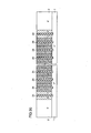
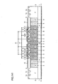
- the configuration of the present invention differs from the configuration shown in Fig. 1 in the point that the present embodiment has a configuration wherein the concentrations of n-type drift regions 3 and p-type impurity regions 4 are independently lowered to get lesser in an alternating manner in the direction toward the edge portion side in four stages without using each combination of n-type drift region 3 and p-type impurity region 4 (hereinafter referred to as a pn combination) as one unit. That is to say, p-type impurity region 4 located at the outermost portion of the pn-repeating structure is a region of extremely low concentration having the lowest impurity concentration.
- n-type drift region 3 adjoining this p-type impurity region 4 at the outermost portion is a low concentration region having the next lowest impurity concentration.
- p-type impurity region 4 adjoining this n-type drift region 3 on the center portion side is a middle concentration region having an impurity concentration lower than the high concentration region of the center portion and higher than the low concentration region.
- the concentration is gradually reduced in multiple stages and, thereby, in practice, the change can be regarded as being continuous without discrete stages.
- the area of a portion having a concentration gradient in the termination portion can be eliminated, even though the electrical field distribution form is slightly distorted in comparison with the configuration, wherein the concentration is reduced in four stages using a unit of a pn combination in the above described first embodiment.
- the area used for the structure of these terminal portions is sufficiently small so that the elimination of the area can be regarded as having no influence. Accordingly, in such a case, a more stable electrical field distribution form can be obtained by reducing the concentration using a unit of a pn combination as in the first embodiment.
- the ratio of the area used for the structure of the termination portion to the entirety of the element becomes high when the pn combination is used as a unit and, thereby, there is a disadvantage wherein the on resistance increases (deteriorates). Accordingly, in such a case, the configuration wherein the concentrations of n-type drift regions 3 and p-type impurity regions 4, without using the pn combination as a unit, are independently lowered is effective, as in the present embodiment.
- the impurity concentration of the high concentration regions 3 and 4 is posited as 100%
- a concentration setting of each region in the case that the concentration gradient has four stages is ideal where the respective impurity concentrations of middle concentration region 4, low concentration region 3 and region of extremely low concentration 4 are equally divided so as to be 75%, 50% and 25%.
- the impurity concentrations need not be reduced in equal steps so that a certain range is allowed to each of the impurity concentrations.
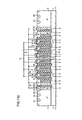
- the configuration of the present embodiment differs from the configuration of the first embodiment in the point wherein the low concentration region at the outermost portion of the pn-repeating structure in the configuration of the present embodiment is formed of only one pair of the pn combination, which is one unit. That is to say, the pair formed of the pn combination 3 and 4 located at the outermost portion of the pn-repeating structure has the same impurity concentration and has an impurity concentration lower than that of the high concentration regions 3 and 4 in the center portion.
- the impurity concentration of each of the low concentration regions 3 and 4 is preferably no less than 30% and no greater than 70% in the case that the impurity concentration of the high concentration regions 3 and 4 is posited as 100%.
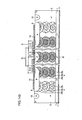
- the configuration of the present embodiment differs from the configuration of the first embodiment in the point that the low concentration region at the outermost portion in the pn-repeating structure is solely p-type impurity region 4 in the present embodiment. That is to say, p-type impurity region 4 at the outermost portion of the pn-repeating structure is solely the low concentration region while other n-type drift regions 3 and p-type impurity regions 4 forming the pn-repeating structure are all high concentration regions.
- the present embodiment has a structure obtained by further simplifying the above described configuration of the third embodiment and, therefore, is effective in, particularly, an element having low voltage, low current and small element area and a manufacturing method for such an element can also be simplified.
- the configuration of the present Embodiment is an example wherein a technique of lowering the concentration in three stages as shown in Fig. 2 and a technique of concentration reduction using the pn combination shown in Fig. 1 as one unit are combined. That is to say, a pair made up of pn combination 3, 4 at the outermost portion in the pn-repeating structure is an extremely low concentration region having the lowest impurity concentration in the pn-repeating structure. A pair made up of pn combination 3, 4 adjoining this extremely low concentration region is a low concentration region having the next lowest impurity concentration. A pair made up of pn combination 3, 4 adjoining this low concentration region is a middle concentration region having the impurity concentration lower than that of the pn combination 3, 4 in the center portion and higher than that of the low concentration region.
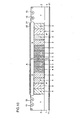
- the configuration of the present embodiment differs from the configurations of the first to fourth embodiments in the configuration of the MOS-FET portion. That is to say, though in the configurations of the first to fourth embodiments, MOS-FET structures are formed on both sides of n-type drift layer 3 in a symmetrical manner, a MOS-FET structure is formed on only one side of n-type drift layer 3 in the present embodiment.
- the MOS-FET structure is formed on only one side of n-type drift region 3 and, therefore, the cell pitch can be scaled down. Therefore, though the total channel width (area) of the MOS-FET is somewhat sacrificed, the cell pitch can be reduced by up to half without changing the total channel width in comparison with the case (the first to fourth embodiments) wherein MOS-FETs are formed in a symmetrical manner and, thereby, an increase in the performance of the pn-repeating structure can be achieved.
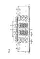
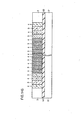
- a plurality of (for example, three) p-type impurity regions 4a forming layers in the depth direction of the semiconductor substrate is integrated so as to form a p-type impurity region 4 making up the pn-repeating structure.
- p-type impurity region 4 located at the outermost portion of the pn-repeating structure from among a plurality of p-type impurity regions 4 has the lowest impurity concentration forming a low concentration region.
- each n-type region in an n- epitaxial layer 2 placed between each pair of the plurality of p-type impurity regions 4 forms an n-type impurity region making up the pn-repeating structure.
- p-type impurity region 4 at the outermost portion in the pn-repeating structure has the lowest impurity concentration in the same manner as in the first embodiment and, therefore, the withstand voltage obtained in this outermost portion becomes high so that an increase in the withstand voltage at the cell portion can be achieved.
- Fig. 6 shows, for the purpose of simplification of the drawing, a configuration wherein the concentration of only one stage respectively on both sides of the terminal portions is lowered.
- the concentration gradient layers of the termination portions may have multiple stages. In the case of the multiple stages, though a withstand voltage higher than that in the case of one stage can be obtained, there is a disadvantage that the process becomes complex as shown in the description of the process flow in the following.
- p-type impurity region 4 has a structure including the concentration distribution in the depth direction of the semiconductor substrate as shown in Fig. 6, a symmetric concentration repeated in the lateral direction is discussed in broad perspective in the present invention and, therefore, a problem caused by such a concentration distribution in the depth direction can be ignored.
- concentration of p-type impurity region 4 in actuality changes without discrete stages and in a continuous manner and changes periodically in the depth direction of the substrate.
- the configuration (Fig. 6) in the present embodiment differs from the configurations of below described Embodiments 7 and 8 in the point that an n - epitaxial layer 2 is used as a substrate in this embodiment, wherein the concentration of the layer has been increased to the degree that the p-type impurity concentration of p-type impurity region 4 is balanced with that of this layer.
- the impurity distribution in a cross section of p-type impurity region 4 becomes of a form well-known in Japan as "round sweet balls of confectionary on a skewer.”
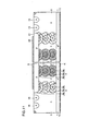
- a plurality of (for example, three) p-type impurity regions 4a that form layers in the depth direction of the semiconductor substrate is integrated as shown in Fig. 7 so as to form p-type impurity regions 4 making up the pn-repeating structure.
- a plurality of (for example, three) n-type impurity regions 3a that form layers in the depth direction of the semiconductor substrate is integrated so as to form n-type drift regions 3 making up the pn-repeating structure. Therefore, each of p-type impurity regions 4 and n-type impurity regions 3 has an impurity concentration distribution that periodically changes in the depth direction of the substrate.
- An average impurity concentration of each of the plurality of p-type impurity regions 4 is substantially the same and an average impurity concentration of each of the plurality of n-type drift regions 3 is also substantially the same.
- This configuration differs from the above described configuration of the sixth embodiment in the point that each of the p-type or n-type regions forming the pn-repeating structure as described above has a constant average concentration and that n-type drift regions 3 are formed through a plurality of 4 implantation steps wherein the implantation energies are changed in the same manner as in p-type impurity regions 4 and, therefore, the concentration distribution in the depth direction of the semiconductor substrate is included in the structure.
- the concentration gradients of n-type drift regions 3 and p-type impurity regions 4 in the depth direction of the semiconductor substrate are depicted as having only two stages for the purpose of simplification in the same manner as in Fig. 6, in actuality they change without discrete stages and in a continuous manner.
- the configuration formed according to a method of diffusing both the p-type impurities and n-type impurities simultaneously so as to form the pn-repeating structure does not become of a form of "round sweet balls of confectionary on a skewer" as shown in Fig. 6.
- the configuration of the seventh embodiment shown in Fig. 8 differs from the conventional configuration of Fig. 7 in the point that the concentration of p-type impurity region 4 at the outermost portion of the pn-repeating structure in the buried multiple epitaxial layers has been lowered by one stage in the configuration of the seventh embodiment.
- the configuration of the eighth embodiment showing Fig. 9 differs from the conventional configuration of Fig. 7 in the point that the concentration of a pair made of the pn combination of p-type impurity region 4 and n-type drift layer 3 at the outermost portion of the pn-repeating structure in the buried multiple epitaxial layers is lowered by one stage in the configuration of the eighth embodiment.
- p-type impurity region 4 (and n-type drift layer 3) at the outermost portion in the pn-repeating structure has the lowest impurity concentration in the same manner as in the first embodiment and, therefore, the withstand voltage obtained at this outermost portion becomes high so that an increase in withstand voltage in the cell portion can be achieved.
- a p-type impurity region 21 is formed on the first main surface side of the entirety of the pn-repeating structure so as to be electrically connected to an anode electrode 22.
- the other parts of the configuration of Fig. 10 are approximately the same as in the configuration shown in Fig. 1
- the other parts of the configuration of Fig. 11 are approximately the same as in the configuration shown in Fig. 6
- the other parts of the configuration of Fig. 12 are approximately the same as in the configuration shown in Fig. 9 and, therefore, the same symbols are attached to the same members, of which the descriptions are omitted.
- the configuration of the twelfth embodiment shown in Fig. 13 differs from the configuration shown in Fig. 5 in the points that a trench 24 is provided in each pn combination in the configuration of the twelfth embodiment and that the MOS-FETs in the configuration of Fig. 5 are replaced with diodes in the configuration of the twelfth embodiment.
- a p-type impurity region 21 is formed on the first main surface side of the entirety of the pn-repeating structure so as to be electrically connected to an anode electrode 22.
- p-type impurity region 4 (and n-type drift layer 3) at the outermost portion has the lowest impurity concentration in the pn-repeating structure in the same manner as in the first embodiment and, therefore, the withstand voltage obtained in this outermost portion becomes high and an increase in the withstand voltage in the cell portion of the diode can be achieved.
- the configurations shown in the ninth to twelfth embodiments are configurations wherein, though the upper portion structures are not active elements, they function as elements that allow high speed switching at a low ON voltage.
- an anode electrode 22 made of metal is electrically connected to the first main surface of the semiconductor substrate and a metal silicide layer 21a is formed on this connection portion.
- the other parts of the configuration of Fig. 14 are approximately the same as in the configuration shown in Fig. 10
- the other parts of the configuration of Fig. 15 are approximately the same as in the configuration shown in Fig. 11
- the other parts of the configuration of Fig. 16 are approximately the same as in the configuration shown in Fig. 12
- the other parts of the configuration of Fig. 17 are approximately the same as in the configuration shown in Fig. 13 and, therefore, the same symbols are attached to the same members, of which the descriptions are omitted.
- p-type impurity region 4 (and n-type drift region 3) at the outermost portion has the lowest impurity concentration in the pn-repeating structure, in the same manner as in the first embodiment and, therefore, the withstand voltage obtained in this outermost portion becomes high so that an increase in the withstand voltage in the cell portion of the Schottky diode can be achieved.
- an n - epitaxial layer 2 is formed on an n+ substrate 1 of a high concentration including arsenic or antimony by means of a conventional epitaxial method.
- This n - epitaxial layer 2 is formed of only one layer having a high and uniform impurity concentration in comparison with the n-type drift layer concentration that is utilized in a MOS-FET of a conventional structure that does not use a multiple RESURF effect.
- a resist pattern 31a having a predetermined pattern is formed on n - epitaxial layer 2 using photomechanical technology. Ion implantation of boron ions is carried out at a high energy level by using this resist pattern 31a as a mask and, thereby, boron ion implanted region 4a is formed at a deep location of the region that becomes the center portion of the pn-repeating structure.
- Fig. 18 shows a case of direct photoresist application wherein a base silicon oxide film is not provided beneath resist pattern 31a a base silicon oxide film may be provided if necessary.
- ion implantation of boron ions is carried out at a middle energy level by using the above described resist pattern 31a as a mask and, thereby, a boron ion implanted region 4a is formed at a location at a depth of a middle level that becomes the center portion of the pn-repeating structure.
- ion implantation of boron ions is carried out at a low energy level by using the above described resist pattern 31a as a mask and, thereby, a boron ion implanted region 4a is formed at a shallow location of a region that becomes the center portion of the pn-repeating structure.
- resist pattern 31a is removed by means of, for example, ashing.
- a resist pattern 31b having a predetermined pattern is formed on n- epitaxial layer 2 using photomechanical technology. Ion implantation of boron ions is carried out at a high energy level by using this resist pattern 31b as a mask and, thereby, a boron ion implanted region 4a is formed at a deep location of a region that becomes the outermost portion of the pn-repeating structure.
- Fig. 21 shows a case of direct photoresist application wherein a base silicon oxide film is not provided beneath resist pattern 31a, a base silicon oxide film may be provided if necessary.
- ion implantation of boron ions is carried out at a middle energy level by using the above described resist pattern 31b as a mask and, thereby, a boron ion implanted region 4a is formed at a location of a middle depth in a region that becomes the outermost portion of the pn-repeating structure.
- ion implantation of boron ions is carried out at a low energy level by using the above described resist pattern 31b as a mask and, thereby, a boron ion implanted region 4a is formed at a shallow location of a region that becomes the outermost portion of the pn-repeating structure.
- resist pattern 31b is removed by means of, for example, ashing.
- the implantation concentration of boron ions implanted into the outermost portion of the pn-repeating structure in the steps of Figs. 21 to 23 is set at approximately half of the implantation concentration of boron ions implanted into the center portion.
- the order of the respective implantations of the above described implantation to a deep location (Fig. 21), implantation to a middle location (Fig. 22) and implantation to a shallow location (Fig. 23) can be switched. Furthermore, the implantation process to give a low concentration to these outermost portions can be switched as a whole with the implantation process to give a high concentration to the above described center portion.
- a resist pattern 31c having a predetermined pattern is formed on an n- epitaxial layer 2 using photomechanical technology. Ion implantation of boron ions is carried out at an extremely low energy level by using this resist pattern 31c as a mask and, thereby, boron ion implanted regions 5 and 15 are formed at very shallow locations of respective regions that become the center portion, the outermost portion and the guard ring portion, which has the termination structure, in the pn-repeating structure. After this, resist pattern 31c is removed by means of, for example, ashing.
- boron ion implanted regions 5 and 15 are diffused to have appropriate sizes so as to form a guard ring portion 15 and a p-type body region 5.
- a plurality of boron ion implanted regions 4a aligned in the depth direction of the semiconductor substrate is diffused into the surroundings so as to be integrated and, thereby, a p-type impurity region 4 making up the pn-repeating structure is formed.
- MOS-FET configuration portions, electrodes, or the like are formed so that the semiconductor device shown in Fig. 6 is completed.
- the maximum acceleration energy is approximately several Mev, even using current high energy ion implantation technology. Therefore, even boron, which is a light element, has a range in Si of 10 ⁇ m, or less, and cannot be implanted into a very deep location. Accordingly, the element structure that can be implemented according to a manufacturing method of the present embodiment is limited to having the comparatively low withstand voltage of approximately 200 V, or less.
- n - epitaxial layer 2 is formed of only one layer having a low concentration and a uniform impurity concentration in comparison with the concentration of n-type drift layers utilized in a MOS-FET of the conventional structure wherein a multiple RESURF effect is not used.
- a resist pattern 31d having a predetermined pattern is formed on n - epitaxial layer 2 using photomechanical technology. Ion implantation of phosphorus ions is carried out at a high energy level by using this resist pattern 31d as a mask and, thereby, an implantation region 3a of phosphorus ions is formed at a deep location in a region that becomes the center portion of the pn-repeating structure.
- Fig. 26 shows a case of direct photoresist application wherein a base silicon oxide film is not provided beneath resist pattern 31d, a base silicon oxide film may be provided if necessary.
- ion implantation of phosphorus ions is carried out at a middle energy level by using the above described resist pattern 31d as a mask and, thereby, an implantation region 3a of phosphorus ions is formed at location of a middle depth in a region that becomes the center portion.
- ion implantation of phosphorus ions is carried out at a low energy level by using the above described resist pattern 31d as a mask and, thereby, an implantation region 3a of phosphorus ions is formed at a shallow location in a region that becomes the center portion. After this, resist pattern 31d is removed by means of, for example, ashing.
- a resist pattern 31e having a predetermined pattern is formed on n - epitaxial layer 2 using photomechanical technology. Ion implantation of boron ions is carried out at a high energy level by using this resist pattern 31e as a mask and, thereby, an implantation region 4a of boron ions is formed at a deep location in a region that becomes the outermost portion of the pn-repeating structure.
- Fig. 29 shows a case of direct photoresist application wherein a base silicon oxide film is not provided beneath resist pattern 31a, a base silicon oxide film may be provided if necessary.
- ion implantation of boron ions is carried out at a middle energy level by using the above described resist pattern 31e as a mask and, thereby, an implantation region 4a of boron ions is formed at a location of a middle depth in a region that becomes the outermost portion of the pn-repeating structure.
- ion implantation of boron ions is carried out at a low energy level by using the above described resist pattern 31e as a mask and, thereby, an implantation region 4a of boron ions is formed at a shallow location in a region that becomes the outermost portion of the pn-repeating structure.
- resist pattern 31e is removed by means of, for example, ashing.
- the implantation concentration of boron ions implanted into the outermost portion of the pn-repeating structure in the steps of Figs. 29 to 31 is set at approximately half of the implantation concentration of boron ions implanted into the center portion.
- guard ring portions 15 and p-type body regions 5 are formed by carrying out the same process as that of the seventeenth embodiment, shown in Fig. 24.
- a plurality of implantation regions 4a of boron ions and a plurality of implantation regions 3a of phosphorus ions aligned in the depth direction of the semiconductor substrate are diffused into the surrounding areas so as to be integrated and p-type impurity regions 4 and n-type drift regions 3 making up the pn-repeating structure are formed.
- MOS-FET configuration portions, electrodes, and the like, are formed so that the semiconductor device shown in Fig. 8 is completed.
- Fig. 32 represents connected n-type drift regions 3 and connected p-type impurity regions 4 in two stages, of low concentration and high concentration, for the purpose of simplification, these impurity concentrations in actuality change without discrete stages and in a continuous manner and change in an alternating manner in the depth direction of the substrate.
- p-type impurity region 4 of a low concentration at the outermost portion of the pn-repeating structure has a wavy cross sectional form that spreads somewhat to the outer periphery in a portion having a high impurity concentration, this detail is omitted for the purpose of simplification.
- p-type impurity regions 4 are formed in n-type epitaxial layer 2 of a comparatively high concentration through boron ion implantation.
- n-type epitaxial layer 2 of a low concentration is used so that respective buried diffusion regions 3a and 4a in n-type drift regions 3 and p-type impurity regions 4 are independently formed. Therefore, the concentration of n-type epitaxial layer 2 in the outer peripheral portion of the pn-repeating structure becomes low so as to form a pin diode.
- the manufacturing method according to the present embodiment is a method suitable for an element of a comparatively high withstand voltage, even among elements having a low withstand voltage.
- ion implantation processes for n-type drift regions 3 and p-type impurity regions 4 are independently carried out and, therefore, there is a disadvantage wherein the number of steps increases in comparison with the seventeenth embodiment. Therefore, it is preferable to choose a method from among these that is appropriate for the element from the point of view of performance or of cost.
- FIG. 9 An example of a manufacturing method for the configuration shown in Fig. 9 is described in reference to Figs. 33 to 42 in the present embodiment. Here, according to the following method, it is possible to form the structure shown in Figs. 1 to 5.
- n - epitaxial layer 2 is formed of only one layer having a low concentration and a uniform impurity concentration in comparison with the concentration of n-type drift layers utilized in a MOS-FET of the conventional structure wherein a multiple RESURF effect is not used.
- a resist pattern 31f having a predetermined pattern is formed on n- epitaxial layer 2 according to photomechanical technology. Ion implantation of phosphorus ions is carried out at a high energy level by using this resist pattern 31f as a mask and, thereby, an implantation region 3a of phosphorus ions is formed at a deep location in a region that becomes the center portion of the pn-repeating structure.
- Fig. 33 shows a case of direct photoresist application wherein a base silicon oxide film is not provided beneath resist pattern 31f, a base silicon oxide film may be provided if necessary.
- ion implantation of phosphorus ions is carried out at a middle energy level by using the above described resist pattern 31f as a mask and, thereby, an implantation region 3a of phosphorus ions is formed at a location of middle depth in a region that becomes the center portion.
- ion implantation of phosphorus ions is carried out at a low energy level by using the above described resist pattern 31f as a mask and, thereby, an implantation region 3a of phosphorus ions is formed at a shallow location in a region that becomes the center portion.
- resist pattern 31f is removed by means of, for example, ashing.
- this is the start of a manufacturing process of a configuration wherein the concentration is required to be lowered.
- a resist pattern 31g having a predetermined pattern is formed on n - epitaxial layer 2 according to photomechanical technology. Ion implantation of phosphorus ions is carried out at a high energy level using this resist pattern 31g as a mask and, thereby, an implantation region 3a of phosphorus ions is formed at a deep location in a region that is closer to the center portion (front) by one stage from the outermost portion of the pn-repeating structure.
- Fig. 36 shows a case of direct photoresist application wherein a base silicon oxide film is not provided beneath resist pattern 31g, a base silicon oxide film may be provided if necessary.
- ion implantation of phosphorus ions is carried out at a middle energy level using the above described resist pattern 31g as a mask and, thereby, an implantation region 3a of phosphorus ions is formed at a location of a middle depth in a region that is closer to the center portion by one stage from the outermost portion of the pn-repeating structure.
- ion implantation of phosphorus ions is carried out at a low energy level using the above described resist pattern 31g as a mask and, thereby, an implantation region 3a of phosphorus ions is formed at a shallow location in a region that is closer to the center portion by one stage from the outermost portion of the pn-repeating structure.
- resist pattern 31g is removed by means of, for example, ashing.
- the implantation concentration of phosphorus ions implanted to the outermost portion of the pn-repeating structure in the process of Figs. 36 to 38 is set at approximately half of the implantation concentration of phosphorus ions implanted to the center portion.
- a resist pattern 31h having a predetermined pattern is formed on n- epitaxial layer 2 using photomechanical technology. Ion implantation of boron ions is carried out at a high energy level using this resist pattern 31h as a mask and, thereby, an implantation region 4a of boron ions is formed at a deep location in a region that becomes the outermost portion of the pn-repeating structure.
- Fig. 39 shows a case of direct photoresist application wherein a base silicon oxide film is not provided beneath resist pattern 31h, a base silicon oxide film may be provided if necessary.
- ion implantation of boron ions is carried out at a middle energy level using the above described resist pattern 31h as a mask and, thereby, an implantation region 4a of boron ions is formed at a location of a middle depth in a region that becomes the outermost portion of the pn-repeating structure.
- ion implantation of boron ions is carried out at a low energy level using the above described resist pattern 31h as a mask and, thereby, an implantation region 4a of boron ions is formed at a shallow location in a region that becomes the outermost portion of the pn-repeating structure.
- resist pattern 31h is removed by means of, for example, ashing.
- the implantation concentration of boron ions implanted to the outermost portion of the pn-repeating structure in the process of Figs. 39 to 41 is set at approximately half of the implantation concentration of boron ions implanted into the center portion.
- the order of the respective implantations of the above described implantation to a deep location (Fig. 39), implantation to a middle location (Fig. 40) and implantation to a shallow location (Fig. 41) can be switched. Furthermore, these implantation processes of a low concentration of boron ions to the outermost portion can be switched as a whole with the above described implantation processes of a high concentration of boron ions or phosphorus ions to the center portion or the implantation process of a low concentration of phosphorus ions to a region closer to the center portion by one stage from the outermost portion of the pn-repeating structure.
- guard ring portions 15 and p-type body regions 5 are formed by carrying out the same process as in the seventeenth embodiment, shown in Fig. 24.
- a plurality of implantation regions 4a of boron ions and a plurality of implantation regions 3a of phosphorus ions aligned in the depth direction of the semiconductor substrate are diffused into the surrounding areas so as to be integrated and p-type impurity regions 4 and n-type drift regions 3 making up the pn-repeating structure are formed.
- MOS-FET configuration portions, electrodes, and the like, are formed so that the semiconductor device shown in Fig. 9 is completed.
- Fig. 42 represents connected n-type drift regions 3 and connected p-type impurity regions 4 in two stages, of low concentration and high concentration, for the purpose of simplification, these impurity concentrations in actuality change without discrete stages and in a continuous manner and change in an alternating manner in the depth direction of the substrate.
- p-type impurity region 4 of a low concentration at the outermost portion of the pn-repeating structure has a wavy cross sectional form that spreads somewhat to the outer periphery in a portion having a high impurity concentration, this detail is omitted for the purpose of simplification.
- a process flow for manufacturing the configuration of Fig. 6 by using multiple epitaxial layers for the formation of the buried regions is described in detail in the twentieth embodiment, in reference to Figs. 43 to 53.
- a first stage of n- epitaxial layer 2a is formed on an n+ substrate 1 of high concentration including arsenic or antimony by means of a conventional epitaxial method.
- This n- epitaxial layer 21 is formed of only one layer having a low concentration and a uniform impurity concentration in comparison with the concentration of n-type drift layers utilized in a MOS-FET of the conventional structure wherein a multiple RESURF effect is not used.
- a resist pattern 31i having a predetermined pattern is formed on n - epitaxial layer 2a using photomechanical technology.
- Fig. 43 shows a case of direct photoresist application wherein a base silicon oxide film is not provided beneath resist pattern 31i, a base silicon oxide film may be provided if necessary.
- ion implantation of boron ions is carried out at a conventional energy level by using this resist pattern 31i as a mask and, thereby, an implantation region 4a of a high concentration of boron ions is formed at a comparatively shallow location (though the location may be deep, in general it is difficult to obtain a high energy level) in a region that becomes the center portion.
- resist pattern 31i is removed by means of, for example, ashing.
- a resist pattern 31k having a predetermined pattern is formed on n - epitaxial layer 2a using photomechanical technology. Ion implantation of boron ions is carried out at a conventional energy level by using this resist pattern 31k as a mask and, thereby, an implantation region 4a of a low concentration of boron ions is formed at a comparatively shallow location in a region that becomes the outermost portion of the pn-repeating structure. After this, resist pattern 31k is removed by means of, for example, ashing.
- Fig. 45 shows a case of direct photoresist application wherein a base silicon oxide film is not provided beneath resist pattern 31k, a base silicon oxide film may be provided if necessary.
- an n - epitaxial layer 2b of a low concentration is formed by means of epitaxial growth in the same manner as the process described in Fig. 43 in order to bury implantation regions 4a of boron ions of both the above described high concentration and low concentration in the substrate.
- each implantation region 4a slightly diffuses into the surrounding area so that the cross sectional form thereof becomes circular as a result of a heat treatment in this epitaxial growth process.
- the diffused state is illustrated in a form of spreading (rising) into the above portion of the epitaxial growth interface shown by the dotted line and this rise, itself, is not positively utilized and the rise is not harmful.
- each of the processes starting from the formation of the above described first stage of n - epitaxial layer 2a, of the formation of a high concentration boron ion implanted region 4a, of the formation of a low concentration boron ion implanted region 4a and of the formation of a second stage of n - epitaxial layer 2b is essentially repeated a desired number of times.
- a resist pattern 311 having a predetermined pattern is formed on n - epitaxial layer 2b using photomechanical technology. Ion implantation of boron ions is carried out at a conventional energy level by using this resist pattern 311 as a mask and, thereby, an implantation region 4a of a high concentration of boron ions is formed at a comparatively shallow location of a region that becomes the center portion of the pn-repeating structure. After this, resist pattern 311 is removed by means of, for example, ashing.
- Fig. 47 shows a case of direct photoresist application wherein a base silicon oxide film is not provided beneath resist pattern 311, a base silicon oxide film may be provided if necessary.
- a resist pattern 31m having a predetermined pattern is formed on n - epitaxial layer 2b using photomechanical technology. Ion implantation of boron ions is carried out at a conventional energy level by using this resist pattern 31m as a mask and, thereby, an implantation region 4a of a low concentration of boron ions is formed at a comparatively shallow location of a region that becomes the outermost portion of the pn-repeating structure. After this, resist pattern 31m is removed by means of, for example, ashing.
- Fig. 48 shows a case of direct photoresist application wherein a base silicon oxide film is not provided beneath resist pattern 31m, a base silicon oxide film may be provided if necessary.
- n - epitaxial layer 2c is formed by means of epitaxial growth in the same manner as described in the process of Fig. 43 in order to bury implantation regions 4a of boron ions of both the above described high concentration and low concentration in the substrate.
- each implantation region 4a slightly diffuses into the surrounding area so that the cross sectional form thereof becomes circular as a result of a heat treatment in this epitaxial growth process.
- the diffused state is illustrated in a form of spreading (rising) into the above portion of the epitaxial growth interface shown by the dotted line and this rise, itself, is not positively utilized and the rise is not harmful.
- a resist pattern 31n having a predetermined pattern is formed on n - epitaxial layer 2c using photomechanical technology. Ion implantation of boron ions is carried out at a conventional energy level by using this resist pattern 31n as a mask and, thereby, an implantation region 4a of a high concentration of boron ions is formed at a comparatively shallow location of a region that becomes the center portion of the pn-repeating structure. After this, resist pattern 3 in is removed by means of, for example, ashing.
- Fig. 49 shows a case of direct photoresist application wherein a base silicon oxide film is not provided beneath resist pattern 31n, a base silicon oxide film may be provided if necessary.
- a resist pattern 31o having a predetermined pattern is formed on n - epitaxial layer 2c using photomechanical technology. Ion implantation of boron ions is carried out at a conventional energy level by using this resist pattern 310 as a mask and, thereby, an implantation region 4a of a low concentration of boron ions is formed at a comparatively shallow location of a region that becomes the outermost portion of the pn-repeating structure. After this, resist pattern 31o is removed by means of, for example, ashing.
- Fig. 50 shows a case of direct photoresist application wherein a base silicon oxide film is not provided beneath resist pattern 31o, a base silicon oxide film may be provided if necessary.
- n - epitaxial layer 2d of a low concentration is formed by means of epitaxial growth in the same manner as described in the process of Fig. 43 in order to bury implantation regions 4a of boron ions of both the above described high concentration and low concentration in the substrate.
- a multi-layer epitaxial layer 2 is formed of n - epitaxial layers 2a to 2d.
- each implantation region 4a slightly diffuses into the surrounding area so that the cross sectional form thereof becomes circular as a result of a heat treatment in this epitaxial growth process.
- the diffused state is illustrated in a form of spreading (rising) into the above portion of the epitaxial growth interface shown by the dotted line and this rise, itself, is not positively utilized and the rise is not harmful.
- a resist pattern 31p having a predetermined pattern is formed on an n - epitaxial layer 2d using photomechanical technology. Ion implantation of boron ions is carried out at an extremely low energy level by using this resist pattern 31p as a mask and, thereby, implantation regions 5 and 15 of boron ions are formed at very shallow locations of the respective regions that become the center portion and the outermost portion of the pn-repeating structure as well as the guard ring portion that has the termination structure. After this, resist pattern 31p is removed by means of, for example, ashing.
- a heat treatment at a high temperature is carried out for a long period of time.
- the implantation regions 5 and 15 of boron ions are diffused so as to have appropriate sizes so that guard ring portions 15 and p-type body regions 5 are formed.
- a plurality of boron ion implanted regions 4a aligned in the depth direction of the semiconductor substrate is diffused into the surroundings so as to be integrated and, thereby, a p-type impurity region 4 making up the pn-repeating structure is formed.
- MOS-FET configuration portions, electrodes, or the like are formed so that the semiconductor device shown in Fig. 6 is completed.
- the implantation concentration of boron ions implanted into the outermost portion of the pn-repeating structure in the steps of Fig. 45, Fig. 48 and Fig. 50 is set at approximately half of the implantation concentration of boron ions implanted into the center portion.
- the concentration of the outermost portion of the pn-repeating structure is lowered by only one stage
- the concentration may be lowered in multiple stages in accordance with the relationship between the price and performance of the required products and the present embodiment is definitely not limited to the structure wherein the concentration is lowered in one stage or to the manufacturing method for such a structure.
- epitaxial layers can, in principle, be infinitely stacked by increasing the number of layers. Therefore, a semiconductor device obtained according to this manufacturing method can deal with withstand voltages in a range of from a middle withstand voltage of several hundreds V to a high withstand voltage of several thousands V. Contrarily, as described below, a heat treatment process at a relatively high temperature is always required in order to connect buried diffusion regions 4a in the depth direction.
- a process flow for manufacturing the configuration of Fig. 6 by using multi-layered epitaxial layer for the formation of a buried region and by using a strip pattern for diffusion at the outermost portion of the pn-repeating structure is described in detail as the twenty-first embodiment in reference to Figs. 54 to 63.
- a first stage of n - epitaxial layer 2a is formed on an n + substrate 1 of a high concentration including arsenic or antimony by means of a conventional epitaxial method.
- This n - epitaxial layer 2a is formed of only one layer having a low concentration and a uniform impurity concentration in comparison with the concentration of the n-type drift layer utilized in a MOS-FET of the conventional structure wherein a multiple RESURF effect is not used.
- a resist pattern 31q having a predetermined pattern is formed on n - epitaxial layer 2a by means of photomechanical technology.
- a first opening pattern including a single hole is formed in a region that becomes the center portion of the pn-repeating structure of this resist pattern 31q while a second opening pattern including a plurality of microscopic holes is formed in a region that becomes the outermost portion of the pn-repeating structure.
- the sum of the areas of the openings of all of the microscopic holes in the second opening pattern is set to be smaller than the area of the opening of the first opening pattern.
- Fig. 54 shows a case of direct photoresist application wherein a base silicon oxide film is not provided beneath resist pattern 31q, a base silicon oxide film may be provided if necessary.
- ion implantation of boron ions is carried out at a conventional energy level by using this resist pattern 31q as a mask.
- an implantation region 4a of a high concentration of boron ions is formed at a comparatively shallow location in a region that becomes the center portion of the pn-repeating structure and an implantation region 4a of a low concentration of boron ions is formed at a comparatively shallow location in a region that becomes the outermost portion of the pn-repeating structure, respectively.
- Fig. 63 shows the state of impurity implantation at the outermost portion of the pn-repeating structure immediately after the above described ion implantation.
- the second opening pattern above the outermost portion of the pn-repeating structure is formed of a plurality of microscopic holes and, therefore, implantation regions 4a 1 of boron ions are formed directly beneath the respective microscopic holes.
- a heat treatment for impurity diffusion is carried out on the substrate in this condition.
- a slight heat treatment makes the plurality of implantation regions 4a 1 of boron ions spread and diffuse into the surrounding areas, as shown in Fig. 64, so as to overlap each other and so as to become integrated to form an implantation region 4a of a low concentration.
- a slight heat treatment enables the respective implantation regions 4a 1 to easily overlap through lateral diffusion so that the concentration becomes uniform as a whole.
- this implantation region 4a of a low concentration has unevenness in form and concentration, it can macroscopically be regarded as a uniform diffusion region 4a of a comparatively low concentration.
- the above described heat treatment itself can be carried out as a part of an epitaxial growth process in the following steps or can be independently carried out before the epitaxial growth.
- the sum of the areas of the openings of all of the microscopic holes in the second opening pattern is set to become smaller than the area of the opening of the first opening pattern. Therefore, even though ion implantation to both of these opening patterns is carried out at the same time, implantation region 4a of a high concentration can be formed in a region that becomes the center portion and implantation region 4a of a low concentration can be formed in a region that becomes the outermost portion of the pn-repeating structure, respectively.
- resist pattern 31q is removed by means of, for example, ashing.
- an n - epitaxial layer 2b of a low concentration is formed through epitaxial growth in the same manner as described in the process of Fig. 54 in order to bury both of the above described implantation regions 4a of boron ions of a high concentration and of a low concentration in the substrate.
- each implantation region 4a slightly diffuses into the surrounding area so that the cross sectional form thereof becomes circular as a result of a heat treatment in this epitaxial growth process.
- the diffused state is illustrated in a form of spreading (rising) into the above portion of the epitaxial growth interface shown by the dotted line and this rise, itself, is not positively utilized and the rise is not harmful.
- the respective steps, starting from the formation of the above described first stage n - epitaxial layer 2a, of the formation of implantation region 4a of a high concentration of boron ions, of the formation of implantation region 4a of a low concentration of boron ions and of the formation of a second stage n - epitaxial layer 2b are essentially repeated a desired number of times.
- a resist pattern 31r having a predetermined pattern is formed on n - epitaxial layer 2a by means of photomechanical technology in the same manner as in Fig. 54.
- a first opening pattern made of a single hole in this resist pattern 31r is formed above a region that becomes the center portion of the pn-repeating structure and a second opening pattern made of a plurality of microscopic holes is formed above a region that becomes the outermost portion of the pn-repeating structure.
- the sum of the areas of the openings of all of the microscopic holes in the second opening pattern is set to be smaller than the area of the opening of the first opening pattern.
- Fig. 57 shows a case of direct photoresist application wherein a base silicon oxide film is not provided beneath resist pattern 31r, a base silicon oxide film may be provided if necessary.
- ion implantation of boron ions is carried out at a conventional energy level by using this resist pattern 31r as a mask.
- an implantation region 4a of a high concentration of boron ions is formed at a comparatively shallow location in a region that becomes the center portion of the pn-repeating structure and an implantation region 4a of a low concentration of boron ions is formed at a comparatively shallow location in a region that becomes the outermost portion of the pn-repeating structure, respectively.
- resist pattern 31r is removed by means of, for example, ashing.
- each implantation region 4a slightly diffuses into the surrounding area so that the cross sectional form thereof becomes circular as a result of a heat treatment in this epitaxial growth process.
- region 4a of a high concentration of boron ions is formed at a comparatively shallow location in a region that becomes the center portion of the pn-repeating structure and an implantation region 4a of a low concentration of boron ions is formed at a comparatively shallow location in a region that becomes the outermost portion of the pn-repeating structure, respectively, by means of a single photomechanical process and a single ion implantation in the same manner as described above.
- resist pattern 31s is removed by means of, for example, ashing.
- each implantation region 4a slightly diffuses into the surrounding area so that the cross sectional form thereof becomes circular as a result of a heat treatment in this epitaxial growth process.
- a resist pattern 31t having a predetermined pattern is formed on n- epitaxial layer 2d by means of photomechanical technology. Ion implantation of boron ions is carried out at an extremely low energy level by using this resist pattern 31t as a mask and, thereby, implantation regions 5 and 15 of boron ions are formed at very shallow locations in the respective regions that become the center portion and the outermost portion of the pn-repeating structure as well as a guard ring portion that is the termination structure. After this, resist pattern 31t is removed by means of, for example, ashing.
- the embodiment is not specifically limited to this and, therefore, the base silicon oxide film is omitted in the drawings for the purpose of simplification.
- a heat treatment at high temperature for a long period of time is carried out.
- implantation regions 5 and 15 of boron ions are diffused to appropriate sizes so that guard ring portion 15 and p-type body region 5 are formed.
- a plurality of implantation regions 4a of boron ions aligned in the depth direction of the semiconductor substrate is diffused to the surrounding areas so as to be integrated and, thereby, a p-type impurity region 4, forming the pn-repeating structure, is formed.
- an n + source region 6 and a p + contact region 7 for making a low resistance contact with a p-type body region 5 are formed within the p-type body region 5 by means of conventional photomechanical technology and by means of ion implantation technology.
- n + source region 6 is formed of arsenic or phosphorus and p + contact region 7 is formed of boron, respectively, and, therefore, it is necessary to independently carry out a photomechanical process and an ion implantation process for forming n + source region 6 and p + contact region 7.
- the order of these processes relative to the below described formation of a gate region is not specifically defined and the order can be switched according to the performance or application.
- the semiconductor device shown in Fig. 6 is completed by completing the MOS-FET structures.
- contact holes via the interlayer insulating film are omitted and Al wires, and the like, are simplified so as to be shown as simple straight line wires.
- the concentration of the outermost portion of the pn-repeating structure is lowered in only one stage is cited as an example and is described, it is possible to lower the concentration in a plurality of stages as in the other above described examples.
- the concentration may be lowered in multiple stages according to the relationship between the price and performance of the required products and the present embodiment is definitely not limited to the structure having one stage or to a manufacturing method for such a structure.
- the manufactured device can cope with a high withstand voltage in a range from a middle withstand voltage of approximately several hundreds V to a high withstand voltage of several thousands V while having the drawback of poor performance in the low withstand voltage region beneath approximately 300 V.
- the outermost portion of the pn-repeating structure can be formed at the same time as the center portion through modification of the manufacturing method of the present embodiment, in contrast to the twentieth embodiment, and, therefore, there is an advantage wherein the manufacturing steps can be halved.
- a process flow for manufacturing a pn-repeating structure in the center portion in the case that there are trenches in the structure is briefly described in the following, though this is not a direct embodiment, and, after that, an embodiment of the present invention wherein the structure having these trenches and a manufacturing method for such a structure are applied is described.
- a process flow for creating diffusion layers in the trench sidewalls through diagonal ion implantation is described sequentially in reference to Figs. 65 to 69.
- anisotropic etching is carried out by using a silicon oxide film, or the like, formed by means of a CVD method as a mask material 41 according to a conventional method and, thereby, a plurality of trenches 23 are created in the first main surface of the semiconductor substrate.
- boron ions are implanted into the sidewalls on only one side of trenches 23 created in a stripe form and, thereby, boron ion implantation regions 4 are formed.
- phosphorus ions are implanted into the sidewalls only on the opposite side of trenches 23 created in a stripe form and, thereby, phosphorus ion implantation regions 3 are formed.
- the steps of these figures 66 and 67 may be switched.
- p-type impurity regions 4 and n-type drift regions 3 having desired impurity concentration profiled are formed by carrying out simultaneous diffusion of boron ion implanted regions 4 and phosphorus ion implantation regions 3 by means of a heat treatment.
- trenches 23 are filled in with an insulator 24, such as a silicon oxide film, formed by means of a CVD method.
- the STM structure is excellent in performance and from the point of view of manufacturing cost in comparison with the buried multi-layer epitaxial structure.
- the technique of diagonal ion implantation into the sidewalls on only one side of trenches 23, which is seldom used for manufacturing LSIs (Large Scale Integrated circuits) is used. Therefore, there is a drawback wherein the process becomes complicated and the difficulty in setting the conditions of manufacture increases at the time when the concentration of the outermost portion in the pn-repeating structure is lowered, in comparison with the case of the above described buried multi-layer epitaxial process. Accordingly, it is preferable to manufacture a semiconductor device of the present invention by selecting a suitable manufacturing method from among several types, including of this embodiment, according to the index listing cost and performance required for the product.
- anisotropic etching is carried out by using a silicon oxide film, or the like, formed by means of a CVD method as a mask material 41a according to a conventional method and, thereby, a plurality of trenches 23 is created in the first main surface of a semiconductor substrate. A trench located at the outermost portion in the finished condition is not included in these trenches 23.
- boron ions are implanted into all of the sidewalls on one side of the plurality of trenches 23 created in a striped form and, thereby, boron ion implanted regions 4 are formed.
- phosphorus ions are implanted into all of the sidewalls on only the opposite side of the plurality of trenches 23 formed in a striped form and, thereby, phosphorus ion implanted regions 3 are formed.
- these processes of Figs. 71 and 72 may be switched and, essentially, the order is not important.
- a window is opened at a desired location of film 41b that is utilized for filling in trenches 23 by means of a conventional photomechanical process and by means of anisotropic etching in order to create a trench at the outermost portion.
- trench 23 at the outermost portion is created by carrying out anisotropic etching on the semiconductor substrate through the window opened in film 41b.
- boron ions are implanted into the sidewall on only one side of trench 23 at the outermost portion so that a boron ion implanted region 4 is formed. At this time, boron ions are implanted having a concentration of approximately half that of the implantation concentration of boron ions that have been implanted in the center portion.
- phosphorus ions are implanted to the sidewall on the opposite side of trench 23 at the outermost portion so that a phosphorus ion implanted region 3 is formed.
- phosphorus ions are implanted having a concentration of approximately half that of the implantation concentration of phosphorus ions that have been implanted in the center portion.
- the step of phosphorus implantation may be switched with the above step of boron implantation and the order thereof is not important.
- a heat treatment is carried out on the entirety of the element so that mesa regions located between trenches 23 have desired concentration distributions.
- boron ion implanted regions 4 and phosphorus ion implanted regions 3 diffuse into the surrounding areas so that p-type impurity regions 4 and n-type drift regions 3 are formed.
- p-type impurity region 4 and n-type drift region 3 diffused from the sidewalls of trench 23 at the outermost portion are set to have lower impurity concentrations than those in the center portion, as described above, and, therefore, the concentrations thereof become lower than the impurity concentrations in the center portion in the finished condition.
- the part of the process up to this point concerns the present embodiment.
- an insulating film 24 is filled in within trenches 23.
- this step of the filling in of the insulating film and the previous heat treatment process may be switched.
- the step of forming comparatively deep diffusion regions, such as a guard ring portion that is the termination structure and p-type body regions of the MOS-FETs is not illustrated, they can be appropriately inserted somewhere in the above described process or somewhere in the back-end process.
- the concentration of only one trench 23 at the outermost portion is lowered is cited as an example and is described, it is possible to lower the concentration in a plurality of stages, as shown in the other above described examples or in the below described example of an STM structure in Fig. 88.
- the concentration may be lowered in multiple stages according to the relationship between price and performance of the required products and the present embodiment is definitely not limited to the structure having one stage or to a manufacturing method for such a structure.
- a manufacturing method in the case that ion implantation of the opposite conductive type, that is to say counter ion implantation, is carried out to the sidewalls of the trench at the outermost portion wherein the concentrations of the diffusion layers are lowered in an STM structure is described in detail as the twenty-third embodiment in reference to Figs. 79 to 86.
- anisotropic etching is carried out by using a silicon oxide film that is formed by means of a CVD method, or the like, as a mask material 41c according to a conventional method and, thereby, a plurality of trenches 23 is simultaneously created in the first main surface of a semiconductor substrate.
- the trench located at the outermost portion in the repeating structure in the finished condition is included in these trenches 23.
- boron ions of the same implantation concentration are implanted into all of the sidewalls on one side of the plurality of trenches 23 created in a striped form and, thereby, boron ion implanted regions 4 are formed.
- phosphorus ions of the same implantation concentration are implanted into all of the sidewalls only on the opposite side of the plurality of trenches 23 created in a striped form and, thereby, phosphorus ion implanted regions 3 are formed.
- the steps of these Figs. 80 and 81 may be switched and the order is not essentially important.
- a film 41d such as a silicon oxide film, formed by means of a CVD method.
- the part of the process up to this point corresponds to a manufacturing method for the conventional STM structure and the following is a process concerning the present embodiment.
- a photoresist pattern 31u having a window above trench 23 located at the outermost portion is formed by means of photomechanical technology. Etching is carried out by using this resist pattern 31u as a mask. In this etching process, wet-type, dry-type etching or a combination of both is appropriately selected according to the absolute depth, the aspect ratio, and the like, of trenches 23 that are to be formed.
- resist pattern 31u is removed by means of, for example, ashing.
- phosphorus ions (n-type) of a conductive type opposite to that of boron (p-type) that was implanted in the previous step is implanted into the sidewall on only one side of trench 23 at the outermost portion and, thereby, a phosphorus ion implanted region 3b is formed.
- This implantation of phosphorus ions controls the finished condition of p-type impurity region 4 formed on the sidewall of trench 23 at the outermost portion to have an impurity concentration of approximately half of the concentration of the impurities that have been implanted in the center portion.
- boron (p-type) of a conductive type opposite to that of phosphorus ions (n-type) that was implanted in the previous step is implanted into the sidewall on only the opposite side of trench 23 at the outermost portion and, thereby, a boron ion implanted region 4b is formed.
- This implantation of boron ions controls the finished condition of n-type impurity region 3 formed on the sidewall of trench 23 at the outermost portion to have an impurity concentration of approximately half of the concentration of the impurities that have been implanted in the center portion.
- the step of boron implantation may be switched with the previous step of phosphorous implantation and the order thereof is not important.
- the part of the process up to this point is characteristic of the present embodiment.
- the same flow of a process of another embodiment is briefly described in the following.
- a heat treatment is carried out on the entirety of the element so that mesa regions placed between trenches 23 have desired concentration distributions.
- boron ion implanted regions 4 and phosphorous ion implanted regions 3 diffuse to the surrounding areas so as to form p-type impurity regions 4 and n-type drift regions 3.
- the impurity concentrations of p-type impurity region 4 and n-type drift region 3 diffused from the sidewalls of trench 23 at the outermost portion are set lower than those of the center portion as described above and, therefore, become lower than those of the center portion in the finished condition.
- an insulating film 24 is filled into trenches 23.
- this process of the filling in of insulating film 24 and the previous heat treatment process may be switched.
- the process of forming comparatively deep diffusion regions such as a guard ring portion that is the termination structure and p-type body regions of MOS-FETs are not illustrated, they can be appropriately inserted somewhere in the above described process or somewhere in the back-end process.
- the concentration of one trench 23 at the outermost portion is lowered is sited as an example and is described, it is possible to lower the concentration in a plurality of stages as shown in the above described other examples or in the below described example of an STM structure in Fig. 88.
- the concentration may be lowered in multiple stages in accordance with the relationship between price and performance of the required products and the present embodiment is definitely not limited to the structure having one stage or to a manufacturing method for such a structure.
- An advantage of the method of the present embodiment is that the process becomes simple in comparison with the case of the twenty-second embodiment wherein trenches 23 are excavated twice.
- trench etching is an established technology, the depth required for this element is in many cases much deeper than that of the trenches utilized in the isolation process of a conventional LSI so that a problem arises that the processing period of time becomes long.
- an advantage is obtained wherein only the buried oxide film is removed in the portion where the counter doping is carried out so that the processing period of time becomes short and the process becomes simple in the case that the process shown in the present embodiment is used.
- the setting of the conditions for either wet-type or dry-type etching is difficult in order to remove the silicon oxide film filled in within a trench of a high aspect ratio.
- FIG. 88 is a three-dimensional bird's-eye view showing a configuration wherein a DLT structure is applied in the trench at the outermost portion in an STM having the structure where the gates are parallel to the trenches shown in Fig. 87.
- the configuration of the present embodiment differs from the configuration shown in Fig. 5 in the point that a trench 23 is provided between a pair made of a p-type impurity region 4 and an n-type drift region 3 in a pn combination in the present embodiment, in the point that the concentration of the pn combination is lowered only in one stage at the outermost portion of the pn-repeating structure of the present embodiment and in the point that trench 23 located at the outermost portion of the plurality of trenches 23 has a DLT structure in the present embodiment.
- the trenches of the DLT structure are trenches wherein a plurality of holes 23a are arranged at intervals in a predetermined direction and, thereby, the trenches have a surface pattern of a dotted line form in the first main surface.
- each trench 23 is filled in with an insulating film 24 made of, for example, a silicon oxide film.
- the present embodiment is characterized by a structure closely related to its manufacturing method wherein the number of the steps is not increased and wherein an element having a high main withstand voltage can be implemented according to the same manufacturing process for an STM having the conventional structure.
- the manufacturing steps increase and become complicated in the case that the concentration gradient in multiple stages is formed in the outermost portion of the pn-repeating structure according to the above described other embodiments
- there is a great advantage wherein the DLT structures shown in the present embodiment and in the following embodiments can be implemented very easily and wherein its manufacturing steps do not generally increase, though the pattern dimensions are restricted, even in the case the concentration is lowered in multiple stages.
- impurity atoms located at the center of a straight line portion (region wherein hole 23a is created) into which impurities are implanted reach to the center portion of a region into which impurities are not implemented.
- the impurity atoms located at an edge (edge of hole 23a) of a straight line portion reach to the edge of the adjoining straight line portion into which impurities are simultaneously implanted.
- the concentration of the straight line portions LA into which impurities are not implanted and the concentration of the regions LB into which impurities are implanted are averaged so as to be lowered to approximately 50% of the concentration immediately after the implantation.
- this Rlc it is preferable for this Rlc to be no less than 30% and no greater than 70%.
- the impurity concentration profile in silicon has a form defined by Gaussian distribution or by error function and can almost be regarded as a primary function, that is to say a triangular distribution, in the case that these distributions are seen on a linear scale. Accordingly, a large gap does not, in fact, occur in the above described approximation and, therefore, the concentration can be very simply adjusted according to the ratio of length LA of the dotted line to interval LB.
- the dimensions in the direction perpendicular to length LA and LB that is to say the width of trenches 23, does not related to this calculation of ratio.
- Fig. 89 shows the condition immediately after implantation or of insufficient heat treatment wherein high concentration regions 3 and 4 still remain in the sidewalls of trenches 23 in the DLT structure and shows the condition wherein diffusion regions 3 and 4 of the dotted line form are not connected.
- Fig. 90 shows the condition wherein impurity regions 3 and 4 have diffused through diffusion in the lateral direction by carrying out a slight heat treatment after implantation.
- High concentration regions diffuse from the sidewalls of trenches 23 in the DLT structure so as to be connected to other high concentration regions 3 and 4 as a result of this heat processing.
- high concentration regions still remain in portions close to the sidewalls of trenches 23 in the DLT structure.
- diffusion by means of a heat treatment is desirable until the entirety has been made uniform, as shown in the below described Fig. 91.
- Fig. 91 shows the state wherein high concentration regions 3 and 4 are sufficiently diffused from the sidewalls of trenches 23 in the DLT structure through lateral direction diffusion by applying a sufficient heat treatment after implantation so as to be connected to other high concentration regions and so that the concentration of the sidewalls of trenches 23 in the DLT structure becomes approximately uniform.
- Table 1 shows an improved effect in the case that the DLT structure is applied to an STM of the 300 V class.
- Fig. 93 is a three-dimensional bird's-eye view showing a configuration wherein a DLT structure is used for three trenches at an outermost portion of the repeating structure in Fig. 92.
- the configuration of the present embodiment differs from the configuration shown in Figs. 87 and 88 in the point that the pn combination of an outermost portion of the pn-repeating structure is lowered in three stages in the present embodiment and in the point the DLT structure is used for three trenches at the outermost portion of the repeating structure in the present embodiment.
- the length and intervals of the dotted lines three trenches 23 at the outermost portion having the DLT structure are adjusted in order to lower the concentration of the pn combination at the outermost portion of the pn-repeating structure in three stages based on the concentration lowering ratio described in the twenty-fourth embodiment.
- the concentration lowering ratio Rlc of trenches 23 of a DLT structure made of a plurality of holes 23a 3 is smaller than the concentration lowering ratio Rlc of trenches 23 of a DLT structure made of a plurality of holes 23a 2 and the concentration lowering ratio Rlc of trenches 23 of a DLT structure made of a plurality of holes 23a 2 is smaller than the concentration lowering ratio Rlc of trenches 23 of a DLT structure made of a plurality of holes 23a 1 .
- the length and intervals of the dotted lines of trenches 23 are adjusted and, thereby, the concentration gradient in multiple stages can easily be formed.
- a process flow in the case that trenches of a DLT structure are used for an STM of a structure where gates are parallel to trenches is described in detail as the twenty-sixth embodiment in reference to Figs. 94 and 95.
- a manufacturing method of the present embodiment follows the same steps as the steps shown in Figs. 79 to 81. Thereby, a plurality of trenches 23 is created in the first main surface and a boron ion implanted region 4 is formed in the sidewall on one side of each trench 23 while a phosphorus ion implanted region 3 is formed in the sidewall on the other side, respectively.
- trenches 23 at the outermost portions on both the left and right sides of the repeating structure are created so as to have a DLT structure.
- a heat treatment is carried out on the entirety of the device so that mesa regions located between trenches 23 have desired concentration distributions.
- boron ion implanted region 4 and phosphorus ion implanted region 3 in the sidewalls of the trench of the DLT structure at an outermost portion of the repeating structure are diffused so that the concentrations thereof are lowered and made uniform and, then, become lower than the impurity concentration of the mesa regions in the center portion.
- an insulator 24 is filled in within each trench 23.
- the step of filling in an insulator and the previous heat treatment step may be switched.
- comparatively deep diffusion regions such as a guard ring or p-type body regions of the MOS-FETs
- the step of forming comparatively deep diffusion regions is not illustrated, it can be appropriately inserted somewhere in the above described steps or somewhere after these steps.
- the process flow may be exactly the same as the above description in the case that the concentration gradient is formed in multiple stages by using this manufacturing process. Thereby, an element of a high withstand voltage having a concentration gradient of multiple stages can be manufactured without increasing the number of manufacturing steps.
- a configuration having a twin trench structure in the center portion and having a MOS-FET structure in the active element portion is described in detail in reference to Fig. 9 and, in addition, a manufacturing method for creating a trench at the outermost portion of a repeating structure through excavation carried out two times is described in detail in reference to Figs. 97 to 105 as the twenty-seventh embodiment.
- the structure of the present embodiment differs from the configuration of Fig. 87 in the point that a mesa portion has a twin trench structure and in the point that the outermost portions of both the left and right sides of the pn-repeating structure are formed of one pair of p-type impurity regions 4 and one pair of n-type impurity regions 3 in order to lower the concentrations.
- twin trench structure is a configuration wherein impurity regions of the same conductive type, respectively, exist in each of the two sidewalls of a trench 23.
- a pair of p-type impurity regions 4 and one pair of n-type impurity regions 3 having impurity concentrations lower than those in the center portion (impurity concentrations of approximately half of those in the center portion) are formed at the outermost portions on both the left and right sides in the pn-repeating structure.
- anisotropic etching is carried out by using a silicon oxide film, or the like, formed by means of a CVD method as a mask material 41e according to a conventional method and, thereby, a first group of trenches made up of a plurality of trenches 23 is created in the first main surface of a semiconductor substrate.
- This first group of trenches does not include trenches located at the outermost portions of the repeating structure in the finished condition.
- phosphorus ions are implanted in the sidewalls on both sides of the entirety of a plurality of trenches 23 forming the first group of trenches so as to have a comparatively high concentration and, then, phosphorous ion implanted regions 3 are formed. After this, film 41e is removed through etching, or the like.
- a film 41f such as a silicon oxide film, is formed by means of a CVD method so as to fill in the entirety of the plurality of trenches 23 of the first group of trenches according to a conventional method.
- This film 41f is patterned by means of photomechanical technology and etching technology. Anisotropic etching is carried out by using the patterned film 41f as a mask material.
- a plurality of trenches 23 forming a second group of trenches is created so that the respective trenches thereof are located in alternation with the respective trenches 23 of the first group of trenches.
- This second group of trenches does not include trenches located at the outermost portions of the repeating structure in the finished condition.
- boron ions are implanted in the sidewalls on both sides of the entirety of a plurality of trenches 23 forming the second group of trenches so as to have a comparatively high concentration and, then, boron ion implanted regions 4 are formed. After this, film 41f is removed through etching, or the like.
- these steps in Figs. 98 and 100 may be switched and the order thereof is not essentially important.
- the process up to this point is a manufacturing method for a conventional type twin trench structure. The following process is a process by which the present embodiment is characterized.
- a film 41g such as a silicon oxide film, is formed by means of a CVD method so as to fill in the entirety of the plurality of trenches 23 of the first and second groups of trenches according to a conventional method.
- This film 41g is patterned by means of photomechanical technology and etching technology so that a portion above an area that is located one stage before the outermost portion in the pn-repeating structure is opened. Anisotropic etching is carried out by using the patterned film 41g as a mask material. Thereby, a first outermost trench 23 is created in a region one stage before the outermost portion of the repeating structure.
- phosphorus ions are implanted into the sidewalls on both sides of the first outermost trench 23 so as to have a comparatively low concentration and, then, phosphorous ion implanted regions 3 are formed. After this, film 41g is removed by means of etching, or the like.
- a film 41h such as a silicon oxide film, is formed by means of a CVD method so as to fill in the entirety of the plurality of trenches 23 of the first and second groups of trenches and the first outermost trench 23 according to a conventional method.
- This film 41h is patterned by means of photomechanical technology and etching technology so that a portion above an area that becomes the outermost portion in the pn-repeating structure is opened. Anisotropic etching is carried out by using the patterned film 41h as a mask material. Thereby, a second outermost trench 23 is created in a region that becomes the outermost portion of the repeating structure.
- boron ions are implanted into the sidewalls on both sides of the second outermost trench 23 so as to have a comparatively low concentration and, then, boron ion implanted regions 4 are formed. After this, film 41h is removed by means of etching, or the like.
- these steps in Figs. 102 and 104 may be switched and the order thereof is not essentially important.
- a film 24, such as a silicon oxide film, is formed by means of a CVD method so as to fill in all of trenches 23 according to a conventional method. After this, a heat treatment is carried out on the entirety of the element so that mesa regions placed between trenches 23 have desired concentration distributions. Thereby, boron ion implanted regions 4 and phosphorous ion implanted regions 3 are diffused into the surrounding areas so that p-type impurity regions 4 and n-type drift regions 3 are formed.
- the concentrations of p-type impurity regions 4 and n-type drift regions 3 that have been diffused from the sidewalls of the first and second outermost trenches 23 are set to be lower than the impurity concentrations in the center portion, as described above, and, therefore, they become lower than the impurity concentrations in the center portion in the finished condition.
- this heat treatment process and the previous step of the filling in of insulating film 24 may be switched.
- a guard ring portion which is the termination structure, and a MOS-FET portion are formed so that the semiconductor device shown in Fig. 96 is completed.
- the length of the repeating pn unit in the pn-repeating structure becomes twice as long as that of the STM structure making it difficult for a three-dimensional multiple RESURF effect to be implemented and, therefore, the main withstanding voltage tends to become lower in the high concentration region even in the ideal case.
- manufacture includes a complex process such that deep trenches are created twice.
- twin trench structure it is not necessary to take into consideration the complex physically phenomenon wherein the effective concentration is lowered due to the diffusion of recoil ions to the opposite side because the same ion species are implanted into both sidewalls of a trench. Therefore, there is an advantage such that the manufacturing margin (process window) is great with respect to the trench form wherein, even in the case of the occurrence of a slight bend or slope, there is no major influence therefrom.
- anisotropic etching is carried out by using a silicon oxide film, or the like, formed by means of a CVD method as a mask material 41i according to a conventional method and, thereby, a first group of trenches made of a plurality of trenches 23 is created in the main surface of a semiconductor substrate.
- This first group of trenches includes a trench located at an outermost portion of the repeating structure in the finished condition.
- phosphorus ions are implanted in the sidewalls on both sides of the entirety of the plurality of trenches 23 forming the first group of trenches so as to have a comparatively high concentration and, then, phosphorous ion implanted regions 3 are formed. After this, film 41i is removed through etching, or the like.
- a film 41j such as a silicon oxide film, is formed by means of a CVD method so as to fill in the entirety of the plurality of trenches 23 of the first group of trenches according to a conventional method.
- This film 41j is patterned by means of photomechanical technology and etching technology. Anisotropic etching is carried out by using the patterned film 41j as a mask material.
- a plurality of trenches 23 forming a second group of trenches is created so that the respective trenches thereof are located in alternation with the respective trenches 23 of the first group of trenches.
- This second group of trenches includes a trench located at an outermost portion of the repeating structure in the finished condition.
- boron ions are implanted into the sidewalls on both sides of the entirety of the plurality of trenches 23 forming the second group of trenches so as to have a comparatively high concentration and, then, boron ion implanted regions 4 are formed. After this, film 41j is removed through etching, or the like.
- these steps in Figs. 107 and 109 may be switched and the order thereof is not essentially important.
- the process up to this point is a manufacturing method for a conventional type twin trench structure. The following process is a process by which the present embodiment is characterized.
- film 41k such as a silicon oxide film, is formed by means of a CVD method so as to fill in the entirety of the plurality of trenches 23 according to a conventional method.
- this film 41k is patterned by means of photomechanical technology and etching technology and, thereby, a portion above a first outermost trench located one stage before the outermost portion of the repeating structure is opened. Anisotropic etching is carried out by using the patterned film 41k as a mask material. Thereby, the filling within first outermost trench 23 is removed.
- boron ions are implanted into the sidewalls on both sides of first outermost trench 23 so as to have a comparatively low concentration and, then, boron ion implanted regions 4b are formed. After this, film 41k is removed by means of etching, or the like.
- a film 411 such as a silicon oxide film, is formed by means of a CVD method so as to fill in all trenches 23 according to a conventional method.
- This film 411 is patterned by means of photomechanical technology and etching technology so that a portion above a second outermost trench 23 located at the outermost portion of the repeating structure is opened. Anisotropic etching is carried out by using the patterned film 411 as a mask material. Thereby, the filling within second outermost trench 23 is removed.
- phosphorus ions are implanted into the sidewalls on both sides of second outermost trench 23 so as to have a comparatively low concentration and, then, phosphorous ion implanted regions 3b are formed. After this, film 41I is removed by means of etching, or the like.
- these steps in Figs. 112 and 114 may be switched and the order thereof is not essentially important.
- a heat treatment is carried out on the entirety of the element so that mesa regions placed between trenches 23 have desired concentration distributions.
- boron ion implanted regions 4 and phosphorous ion implanted regions 3 are diffused into the surrounding areas so that p-type impurity regions 4 and n-type drift regions 3 are formed.
- impurities of opposite conductive types cancel each other through counter doping.
- the impurity concentrations of impurity regions 3 and 4 located in the sidewalls of first and second outermost trenches 23 becomes lower than the impurity concentrations in the center portion.
- this heat processing step and the previous step of filling in of insulating film 24 may be switched.
- a guard ring portion which is the termination structure, and the MOS-FET portions are formed so that the semiconductor device shown in Fig. 96 is completed.
- the length of the repeating pn unit in the pn-repeating structure becomes twice as long as that of the STM structure making it difficult for a three-dimensional multiple RESURF effect to be implemented and, therefore, the main withstanding voltage tends to become lower in the high concentration region even in the ideal case.
- manufacture includes a complex process such that deep trenches are created twice.
- twin trench structure it is not necessary to take into consideration the complex physically phenomenon wherein the effective concentration is lowered due to the diffusion of recoil ions to the opposite side and a uniform concentration profile from the top to the bottom of the trenches can be obtained because the same ion species are implanted into both sidewalls of a trench. Therefore, there is an advantage such that the manufacturing margin (process window) is great with respect to the trench form wherein, even in the case of the occurrence of a slight bend or slope, there is no major influence therefrom.
- the configuration of the present embodiment shares with the configuration shown in Fig. 96 the point that the center portion has a twin trench structure and the active element portion has a MOS-FET structure and differs from the configuration shown in Fig. 96 in the point that the concentration of only a pair of p-type impurity regions 4 at the outermost portion in the pn-repeating structure is lowered in the present embodiment.
- the configuration of the present embodiment is a configuration wherein the concentration of only the p-type impurity regions at the outermost portion of the pn-repeating structure is lowered in only one stage and, therefore, has an advantage that the manufacture thereof is easy.
- the configuration of the present embodiment can be implemented according to the above described twenty-seventh embodiment or the twenty-eighth embodiment and can also be implemented according to the below described thirty-third embodiment.
- the configuration of the present embodiment shares the point that the center portion has a twin trench structure with the configuration shown in Fig. 96 and differs from the configuration shown in Fig. 96 in the point that the active element portion has a pin diode structure in stead of a MOS-FET structure and in the point that the concentration of only a pair of p-type impurity regions 4 at the outermost portion of the repeating structure is lowered.
- the pin diode is formed of a p-type impurity region 21 that is formed on the first main surface side of the entirety of the pn-repeating structure and that is electrically connected to an anode electrode 22.
- the configuration of the present embodiment can be implemented according to the above described twenty-seventh embodiment or the twenty-eighth embodiment and can also be implemented according to the below described thirty-third embodiment.
- the configuration of the present embodiment shares the point that the center portion has a twin trench structure with the configuration shown in Fig. 96 and differs from the configuration shown in Fig. 96 in the point that the active element portion has a Schottky barrier diode structure instead of a MOS-FET structure and in the point that the concentration of only a pair of p-type impurity regions 4 at the outermost portion of the pn-repeating structure in the present embodiment.
- the Schottky barrier diode is formed of the entirety of the pn-repeating structure on the first main surface side that is electrically connected to an anode electrode 22 via a metal silicide layer 21a
- the configuration of the present embodiment can be implemented according to the above described twenty-seventh embodiment or the twenty-eighth embodiment and can also be implemented according to the below described thirty-third embodiment.
- the configuration of the present embodiment shares with the configuration shown in Fig. 96 the point that the center portion has a twin trench structure and the active element portion has a MOS-FET structure and differs from the configuration shown in Fig. 96 in the point that an active element is not provided above a pair of p-type impurity regions 4 at the outermost portion in the pn-repeating structure in the present embodiment.
- p-type impurity regions 21 are formed above the pair of p-type impurity regions 4 at the outermost portion of the pn-repeating structure and are electrically connected to a source electrode 10.
- a manufacturing method of simultaneously forming high concentration regions in the center portion and low concentration regions at the outermost portion of the pn-repeating structure through one ion implantation by using a DLT structure for the twin trench structure is described in detail as the thirty-third embodiment in reference to Figs. 106 to 110.
- anisotropic etching is carried out by using a silicon oxide film, or the like, formed by means of a CVD method as a mask material 41i according to a conventional method and, thereby, a first group of trenches including a plurality of trenches 23 in the center portion and trenches 23 of a DLT structure placed outside thereof is simultaneously created in the first main surface of a semiconductor substrate.
- the number of trenches 23 of a DLT structure may be any number that is no less than one.
- phosphorous ions are implanted into the sidewalls on both sides of the entirety of the plurality of trenches 23 forming the first group of trenches so that phosphorous ion implanted regions 3 are formed.
- film 41i is removed by means of etching, or the like.
- a film 41j such as a silicon oxide film is formed by means of a CVD method so as to fill in the entirety of the plurality of trenches 23 of the first group of trenches.
- This film 41j is patterned by means of photomechanical technology and etching technology. Anisotropic etching is carried out by using the patterned film 41j as a mask material.
- a plural number of trenches 23 in the center portion and trenches 23 of a DLT structure placed outside thereof are created forming a second group of trenches so as to located in alternation with the respective trenches 23 of the first group of trenches.
- the number of trenches 23 of a DLT structure may be any number that is no less than one.
- boron ions are implanted into the sidewalls on both sides of the entirety of the plurality of trenches 23 forming the second group of trenches so that boron ion implanted regions 4 are formed.
- film 41j is removed by means of etching, or the like.
- these steps in Figs. 107 and 109 may be switched and the order thereof is not essentially important.
- a film 41k such as a silicon oxide film is formed by means of a CVD method so as to fill in the entirety of the plurality of trenches 23 according to a conventional method.
- the step of the filling in of an insulator and the previous heat treatment step may be switched.
- a manufacturing method for a pn-repeating structure having bi-pitch units wherein p-type impurity regions and n-type drift regions are formed through separate ion implantations is described in detail in reference to Figs. 120 to 128.
- a manufacturing method of the present embodiment follows the step shown in Fig. 79. Thereby, a plurality of trenches 23 is created in the main surface of a semiconductor substrate.
- a film 41m such as a silicon oxide film is formed by means of a CVD method so as to fill in all trenches 23 according to a conventional method.
- this film 41m is patterned by means of photomechanical technology and etching technology so that a portion above every other trench 23 from among the plurality of trenches 23 is opened.
- Anisotropic etching is carried out by using the patterned film 41m as a mask material. Thereby, the filling within every other trench 23 is removed. Phosphorous ions are implanted into the sidewalls on both sides of every other trench 23 from which the filling has been removed so as to have a comparatively high concentration and, then, phosphorous ion implanted regions 3 are formed.
- film 41m is removed by means of etching, or the like.
- a film 41n such as a silicon oxide film is formed by means of a CVD method so as to fill in all trenches 23 according to a conventional method.
- This film 41n is patterned by means of photomechanical technology and etching technology so that respective portions above the other set of every other trench 23 are opened. Anisotropic etching is carried out by using the patterned film 41n as a mask material. Thereby, the filling within the other set of every other trench 23 is removed.
- Boron ions are implanted into the sidewalls on both sides of the other set of every other trench 23 from which the filling has been removed so as to have a comparatively high concentration and, then, boron ion implanted regions 4 are formed. After this, film 41n is removed by means of etching, or the like.
- these steps in Figs. 121 and 122 may be switched and the order thereof is not essentially important.
- a film 41o such as a silicon oxide film is formed by means of a CVD method so as to fill in all trenches 23 according to a conventional method.
- the process up to this point is a process for forming a structure having the repetition of the same bi-pitch units as in a twin trench structure of a conventional structure and the following process is a process for forming a concentration lowering structure at the outermost portion of the pn-repeating structure according to the present embodiment.
- this film 41o is patterned by means of photomechanical technology and etching technology so that a portion above a first outermost trench 23 located one stage before the outermost portion of the repeating structure is opened. Anisotropic etching is carried out by using the patterned film 41o as a mask material. Thereby, the filling within first outermost trench 23 is removed.
- boron ions are implanted into the sidewalls on both side of first outermost trench 23 so as to have a comparatively low concentration (concentration of approximately half of the impurity concentration of phosphorous ion implanted regions 3) so that boron ion implanted regions 4b are formed.
- film 41o is removed by means of etching, or the like.
- a film 41p such as a silicon oxide film is formed by means of a CVD method so as to fill in all trenches 23 according to a conventional method.
- This film 41p is patterned by means of photomechanical technology and etching technology so that a portion above a second outermost trench 23 located at the outermost portion of the repeating structure is opened. Anisotropic etching is carried out by using the patterned film 41p as a mask material. Thereby, the filling within second outermost trench 23 is removed.
- phosphorous ions are implanted into the sidewalls on both side of second outermost trench 23 so as to have a comparatively low concentration (concentration of approximately half of the impurity concentration of boron ion implanted regions 4) so that phosphorous ion implanted regions 3b are formed.
- film 41p is removed by means of etching, or the like.
- a film 24 such as a silicon oxide film is formed by means of a CVD method so as to fill in all trenches 23 according to a conventional method.
- a heat treatment is carried out on the entirety of the element so that mesa regions placed between trenches 23 have desired concentration distributions.
- the impurities of boron ion implanted regions 4 and phosphorous ion implanted regions 3 are diffused into the surrounding areas so that p-type impurity regions 4 and n-type drift regions 3 are formed.
- the impurities of opposite conductive types cancel each other because of counter doping in the sidewalls of first and second outermost trenches 23.
- the impurity concentrations of impurity regions 3 and 4 located in the sidewalls of first and second outermost trenches 23 become lower than the impurity concentration in the center portion.
- this heat treatment process and the previous process of the filling in of insulating film 24 may be switched.
- guard ring portion that is the termination structure and MOS-FET portions are formed so that the semiconductor device shown in Fig. 96 is completed.
- the above described step of counter doping may be repeated a plurality of times.
- a manufacturing method wherein a method of one-time excavation for the creation of a trench and of separately implanting ions for p-type impurity regions and n-type drain regions only through bi-pitch implantations is used for a trench of a DLT structure at the outermost portion of the repeating structure, is described in detail in reference to Figs. 120 to 123.
- a first group of trenches made of a plurality of trenches 23 in the center portion and trenches 23 of a DLT structure placed outside thereof and a second group of trenches made of a plurality of trenches 23 in the center portion and trenches 23 of a DLT structure placed outside thereof are created in the first main surface of a semiconductor substrate.
- the respective trenches 23 of the first group of trenches and the respective trenches 23 of the second group of trenches are created so as to be positioned in alternation.
- the respective numbers of trenches 23 of a DLT structure of the first and second groups of trenches may be any number that is no less than one
- a film 41m such as a silicon oxide film is formed by means of a CVD method so as to fill in all trenches 23 according to a conventional method.
- this film 41m is patterned by means of photomechanical technology and etching technology so that a portion above every other trench 23 from among the plurality of trenches 23 is opened.
- Anisotropic etching is carried out by using the patterned film 41m as a mask material. Thereby, the filling within every other trench 23 is removed. Phosphorous ions are implanted into the sidewalls on both sides of every other trench 23 from which the filling has been removed so that phosphorous ion implanted regions 3 are formed.
- film 41m is removed by means of etching, or the like.
- a film 41n such as a silicon oxide film is formed by means of a CVD method so as to fill in all trenches 23 according to a conventional method.
- This film 41n is patterned by means of photomechanical technology and etching technology so that respective portions above the other set of every other trench 23 from among the plurality of trenches 23 are opened.
- Anisotropic etching is carried out by using the patterned film 41n as a mask material. Thereby, the filling within the other set of every other trench 23 is removed.
- Boron ions are implanted into the sidewalls on both sides of the other set of every other trench 23 from which the filling has been removed so that boron ion implanted regions 4 are formed. After this, film 41n is removed by means of etching, or the like.
- these steps in Figs. 121 and 122 may be switched and the order thereof is not essentially important.
- a film 41o such as a silicon oxide film is formed by means of a CVD method so as to fill in all trenches 23 according to a conventional method.
- the step of the filling in of an insulator and the previous heat treatment step may be switched.
- a manufacturing method for forming a low concentration region at the outermost portion of the repeating structure through high energy ion implantations of multiple stages in an STM structure is described in detail as the thirty-sixth embodiment in reference to Figs. 129 to 136.
- the manufacturing method of the present embodiment first follows the process shown in Figs. 70 to 72. Thereby, a plurality of trenches 23 is created and phosphorous ion implanted regions 3 and boron ion implanted regions 4 are formed in the sidewalls of the respective trenches 23.
- a film 41q such as a silicon oxide film, is formed by means of a CVD method so as to fill in all trenches 23 according to a conventional method.
- the process up to this point is the same as a method shown in the other above described embodiments.
- the respective implanted regions 3 and 4 may be diffused from the sidewalls of trenches 23 by carrying out a heat treatment, a heat treatment is not carried out on this example.
- a resist pattern 31v having a predetermined pattern is formed on film 41q by means of photomechanical technology. Ion implantation of phosphorus ions is carried out at a high energy level by using this resist pattern 31v as a mask and, thereby, phosphorous ion implanted regions 3a are formed at deep locations of the outermost portion of the pn-repeating structure or of a region one stage before the outermost portion.
- ions can, if necessary, be implanted after film 41q is etched or resist pattern 31v can also be removed so that ions are implanted by using only the pattern of film 41q as a mask.
- ion implantation of phosphorus ions is carried out at a middle energy level by using the above described resist pattern 31v as a mask and, thereby, phosphorous ion implanted regions 3a are formed at locations of a middle depth of the outermost portion of the pn-repeating structure or of a region one stage before the outermost portion.
- ion implantation of phosphorus ions is carried out at a low energy level by using the above described resist pattern 31v as a mask and, thereby, phosphorous ion implanted regions 3a are formed at shallow locations of the outermost portion of the pn-repeating structure or of a region one stage before the outermost portion.
- resist pattern 31v is removed by means of, for example, ashing.
- the implantation concentration of phosphorus ions that are implanted in the outermost portion of the pn-repeating structure or in a region one stage before the outermost portion in the steps of Figs. 130 to 132 is approximately half of the implantation concentration of phosphorus ions that have been implanted in the center portion.
- the order of the respective implantations which are the above described implantation to a deep location (Fig. 130), the implantation to a location of a middle depth (Fig. 131) and the implantation to a shallow location (Fig. 132), can be switched. Furthermore, the process of phosphorus ion implantation into the outermost portion of the pn-repeating structure or into a region one stage before the outermost portion can be switched as a whole with the above described implantation process of boron ions or phosphorus ions into the center portion.
- ion may be implanted in two stages or in one stage in the case that an element of a class wherein withstand voltage is low has a thin epitaxial layer and, contrarily, in some cases ions are implanted in four, or more, stages in the case that an element of a class wherein withstand voltage is high has a thick epitaxial layer. Therefore, the present embodiment is not limited to having three stages.
- resist pattern 31w having a predetermined pattern, is formed on film 41q by means of photomechanical technology. Ion implantation of boron ions is carried out at a high energy level using this resist pattern 31w as a mask and, thereby, boron ion implanted regions 4a are formed at deep locations of the outermost portion in the pn-repeating structure or a region one stage before the outermost portion.
- ions can be implanted after film 41q is etched or ions can be implanted after resist pattern 31w is also removed so that only the pattern of film 41q is used as a mask, if necessary.
- ion implantation of boron ions is carried out at a middle energy level by using the above described resist pattern 31w as a mask and, thereby, boron ion implanted regions 4a are formed at locations of a middle depth of the outermost portion of the pn-repeating structure or of a region one stage before the outermost portion.
- ion implantation of boron ions is carried out at a low energy level by using the above described resist pattern 31w as a mask and, thereby, boron ion implanted regions 3a are formed at shallow locations of the outermost portion of the pn-repeating structure or of a region one stage before the outermost portion.
- resist pattern 31w is removed by means of, for example, ashing.
- the implantation concentration of boron ions that are implanted in the outermost portion of the pn-repeating structure or in a region one stage before the outermost portion in the steps of Figs. 133 to 135 is approximately half of the implantation concentration of boron ions that have been implanted in the center portion.
- the order of the respective implantations which are the above described implantation to a deep location (Fig. 133), the implantation to a location of a middle depth (Fig. 134) and the implantation to a shallow location (Fig. 135), can be switched. Furthermore, the process of boron ion implantation for giving a low concentration into the outermost portion of the pn-repeating structure or into a region one stage before the outermost portion can be switched as a whole with the above described implantation process of boron ions or phosphorus ions for giving a high concentration into the center portion or implantation process of phosphorus ions for giving a low concentration into the outermost portion of the pn-repeating structure or into a region one stage before the outermost portion.
- these processes are not limited to the ion implantations for lowering the concentration in three stages and the number of stages may be greater or smaller than this in the same manner in the above described phosphorous ion implanted regions 3a.
- a heat treatment is carried out and, thereby, the respective impurities of a plurality of boron ion implanted regions 4a and a plurality of phosphorous ion implanted regions 3a aligned in the depth direction of the semiconductor substrate are diffused into the surrounding areas so as to be integrated and, then, p-type impurity regions 4 and n-type drift regions 3 forming the pn-repeating structure are formed.
- MOS-FET formation portions, electrodes, and the like are formed.
- the connected n-type drift regions 3 and p-type impurity regions 4 are represented in two stages of a low concentration and of a high concentration for the purpose of simplification, in actuality, the concentration changes without discrete stages and in a continuous manner.
- the p-type impurity region 4 of a low concentration at the outermost portion of the pn-repeating structure has a wavy cross sectional form that spreads somewhat to the outer periphery in a portion having a high impurity concentration, this detail is omitted for the purpose of simplification.
- a manufacturing method in the case that high energy ion implantation is carried out in multiple stages at the time when the concentration is lowered at the outermost portion of the pn repeating structure in an STM structure and in the case that a p-type impurity region is located at the outermost portion of the pn-repeating structure is described in detail as the thirty-seventh embodiment in reference to Figs. 137 to 140.
- the manufacturing method of the present embodiment first, follows the steps shown in Figs. 70 to 72 and, after that, follows the additional steps of Figs. 129 to 132. Thereby, a plurality of trenches 23, phosphorous ion implanted regions 3 and boron ion implanted regions 4 formed in the sidewalls on both sides of respective trenches 23, a film 41q filling in respective trenches 23 and a phosphorus ion implanted region 3a located one stage before the outermost portion of the pn-repeating structure are formed.
- a resist pattern 31x having a predetermined pattern is formed on film 41q by means of photomechanical technology. Ion implantation of boron ions is carried out at a high energy level using this resist pattern 31x as a mask and, thereby, a boron ion implanted region 4a is formed at a deep location in a region that becomes the outermost portion of the pn-repeating structure.
- ions can be implanted after film 41q is etched or ions can be implanted after removing resist pattern 31x so that only the pattern of film 41q is used as a mask.
- ion implantation of boron ions is carried out at a middle energy level using the above described resist pattern 31x as a mask and, thereby, a boron ion implanted region 4a is formed at a location of a middle depth in a region that becomes the outermost portion of the pn-repeating structure.
- ion implantation of boron ions is carried out at a low energy level using the above described resist pattern 31x as a mask and, thereby, a boron ion implanted region 4a is formed at a shallow location in a region that becomes the outermost portion of the pn-repeating structure.
- resist pattern 31x is removed by means of, for example, ashing.
- the implantation concentration of boron ions implanted in the outermost portion of the pn-repeating structure in the steps of Figs. 137 to 139 is set at approximately half the implantation concentration of boron ions implanted into the center portion.
- the order of the respective implantations which are the above described implantation into a deep location (Fig. 137), implantation into a middle location (Fig. 138) and implantation into a shallow location (Fig. 139), can be switched. Furthermore, these implantation steps of boron ions of a low concentration into the outermost portion can be switched as a whole with the above described implantation steps of boron ions or phosphorus ions of a high concentration into the center portion or with the implantation steps of phosphorus ions of a low concentration into a region one stage closer to the center portion from the outermost portion of the pn-repeating structure.
- these steps are not limited to the ion implantations in three stages but, rather, the number of ion implantations may be greater than, or fewer than, this in the same manner as in the above described ion implantations into phosphorus ion implanted region 3a.
- a heat treatment is carried out and, thereby, the plurality of boron ion implanted regions 4a and the plurality of phosphorous ion implanted regions 3a aligned in the depth direction of the semiconductor substrate, respectively, are diffused into the surrounding areas so as to be integrated and, thereby, p-type impurity region 4 and n-type drift region 3 forming the pn-repeating structure are formed.
- MOS-FET configuration portions, electrodes, and the like are formed.
- n-type drift regions 3 and p-type impurity regions 4 are represented in Fig. 140 as having two stages, of a low concentration and a high concentration for the purpose of simplification, in actuality the concentration changes without discrete stages and in a continuous manner.
- p-type impurity region 4 of a low concentration at the outermost portion of the pn-repeating structure has a wavy cross sectional form that spreads somewhat to the outer periphery in a portion having a high impurity concentration, the detailed description of this is omitted for the purpose of simplification.
- the configuration of the thirty-eighth embodiment shares with the configuration of Fig. 3 the point that the concentration is lowered in only one pair (one stage) made up of p-type impurity region 4 and n-type drift region 3 at the outermost portion, on both the left and right sides, of the pn-repeating structure and differs from the configuration of Fig. 3 in the point that a MOS-FET, which is an active element, is not formed above the regions wherein the concentration is lowered in the present embodiment.
- p-type impurity regions 5 are formed above p-type impurity regions 4 and n-type drift regions 3 of a low concentration at the outermost portions of the pn-repeating structure and are electrically connected to source electrodes 10 while n + source regions 6 and gate electrodes 9, which are components of MOS-FETs, are not formed in the present embodiment.
- the configuration of the thirty-ninth embodiment shares with the configuration of Fig. 87 the point that the concentration is lowered in only one pair (one stage) made of p-type impurity region 4 and n-type drift region 3 at the outermost portion of the pn-repeating structure in the STM having a structure wherein gates are parallel to trenches and differs from the configuration of Fig. 87 in the point that a MOS-FET, which is an active element, is not formed above the region wherein the concentration is lowered in the present embodiment.
- p-type impurity regions 21 are formed above p-type impurity regions 4 and n-type drift regions 3 of a low concentration at the outermost portions of the pn-repeating structure and are electrically connected to source electrodes 10 while n + source regions 6 and gate electrodes 9, which are components of MOS-FETs, are not formed in the present embodiment.
- the configuration of the fortieth embodiment shares with the configuration of Fig. 6 the point that the concentration is lowered in only p-type impurity region 4 at outermost portion of the pn-repeating structure in the buried multi-layer epitaxial structure and differs from the configuration of Fig. 6 in the point that a MOS-FET, which is an active element, is not formed above the region wherein the concentration is lowered.
- p-type impurity regions 5 are formed above p-type impurity regions 4 of a low concentration at the outermost portions of the pn-repeating structure and are electrically connected to source electrodes 10 while n + source regions 6 and gate electrodes 9, which are components of MOS-FETs, are not formed in the present embodiment.
- a configuration wherein the concentration is lowered at the outermost portion of the pn-repeating structure of a horizontal power MOS-FET mounted on an SOI (Silicon On Insulator) substrate is described in detail as the forty-first embodiment in reference to Figs. 144 and 145.
- a semiconductor layer 60 is formed above a silicon substrate 51 via an insulating film 52, such as a silicon oxide film. Then, a horizontal power MOS-FET having a pn-repeating structure, wherein the concentration is lowered at the outermost portion, is formed according to the present invention.
- p-type impurity regions 4 and n-type impurity regions 3 are formed in alternation so as to form a pn-repeating structure in this semiconductor layer 60. Then, the concentration is lowered in two stages at the outermost portion of this pn-repeating structure having one pair made up of a pn combination as one unit, as shown in Fig. 145.
- p-type region 5 is formed so as to form a pn junction with n-type impurity regions 3 and so as to be electrically connected to p-type impurity regions 4.
- n + source regions 6 are formed so that portions of p-type region 5 are placed between n + source regions 6 and n-type impurity regions 3.
- a gate electrode layer 9 is formed so as to face p-type region 5 placed between n-type impurity regions 3 and n + source regions 6 via a gate insulating layer 8. This gate electrode layer 9 extends in the direction of pn repetition above the first main surface.
- n + region 54 and an nb region 53 are formed on the side opposite to p-type region 5 of the pn-repeating structure and n + region 54 is electrically connected to a drain electrode.
- trenches may be provided between p-type impurity regions 4 and n-type impurity regions 3 in the above described pn-repeating structure and, in this case, trenches 23 filled in with insulators 24, or the like, are located between p-type impurity regions 4 and n-type impurity regions 3, as shown in Figs. 146 and 147.
- the region wherein the concentration is lowered at the outermost portion of the pn-repeating structure is formed by carrying out a counter ion implantation (counter doping) in the sidewalls of the trench located at the edge portion of the repeating structure.
- impurities of the same conductive type as the impurities that have already been implanted into the sidewalls of the trenches located in the center portion of the pn-repeating structure are additionally implanted and, thereby, the concentrations of p layers 4 and n layers 3 of the pn-repeating structure in the center portion are enhanced so that the concentration of the impurity region in the sidewall of the trench at the outermost portion of the repeating structure may become relatively low.
- first, p-type impurity regions 4 and n-type impurity regions 3 of a comparatively low concentration are formed in the sidewalls of trenches 23 by following the steps of Figs. 79 to 81. After this, the filling within trenches 23 in the center portion of pn-repeating structure is removed. Then, additional p-type impurities are implanted into p-type impurity regions 4 in the sidewalls on one side of these trenches 23 in the center portion and additional n-type impurities are implanted into n-type impurity regions 3 in the sidewalls on the other side.
- the concentrations of p-type impurity regions 4 and n-type impurity regions 3 in the sidewalls of trenches 23 in the center portion of the repeating structure are enhanced so that impurity regions 3 and 4 in the sidewalls of trench 23 at the outermost portion of the repeating structure become relatively low concentration regions.
- p-type impurity regions 4 and n-type impurity regions 3 of a comparatively low concentration are formed in the sidewalls of trenches 23 by following the steps of Figs. 106 to 110. After this, the filling within trenches 23 in the center portion of pn-repeating structure is removed. Then, additional p-type impurities are implanted in p-type impurity regions 4 in the sidewalls on both sides of trenches 23 in this center portion and additional n-type impurities are implanted into n-type impurity regions 3 in the sidewalls on both sides of other trenches 23 in the center portion.
- the concentrations of p-type impurity regions 4 and n-type impurity regions 3 in the sidewalls of trenches 23 in the center portion of the repeating structure are enhanced so that impurity regions 3 and 4 in the sidewalls of trench 23 at the outermost portion of the repeating structure become relatively low concentration regions.
- p-type impurity regions and n-type impurity regions 3 of a comparatively low concentration are formed in the sidewalls of trenches 23 by following the steps of Figs. 120 to 123. After this, the filling within trenches 23 in the center portion of pn-repeating structure is removed. Then, additional p-type impurities are implanted in p-type impurity regions 4 in the sidewalls on both sides of trenches 23 in this center portion and additional n-type impurities are implanted into n-type impurity regions 3 in the sidewalls on both sides of other trenches 23 in the center portion.
- the concentrations of p-type impurity regions 4 and n-type impurity regions 3 in the sidewalls of trenches 23 in the center portion of the repeating structure are enhanced so that impurity regions 3 and 4 in the sidewalls of trench 23 at the outermost portion of the repeating structure become relatively low concentration regions.
- the concentration of the impurity region located at the outermost portion of the pn-repeating structure is lower than that in the center portion
- the same effect can be obtained by setting the general effective charge amount of the impurity region located at the outermost portion of the pn-repeating structure to be smaller than that in the center portion, as described in the first embodiment.
- the main withstanding voltage of a power semiconductor device wherein a three-dimensional multiple RESURF principle with an element withstand voltage in a broad range of 20 V to 6000 V is specifically applied can be improved and the tradeoff relationship between the main withstanding voltage and the ON resistance can also be improved so that an inexpensive semiconductor device having a low power loss and having a small chip size can be obtained.
- the present invention can be advantageously applied to a power semiconductor device and a manufacturing method for the same wherein a three-dimensional multiple RESURF principle with a element withstand voltage in a broad range of 20 V to 6000 V is specifically applied.
Landscapes
- Insulated Gate Type Field-Effect Transistor (AREA)
- Thyristors (AREA)
- Metal-Oxide And Bipolar Metal-Oxide Semiconductor Integrated Circuits (AREA)
Abstract
Description
wherein the process becomes more complicated and the manufacturing cost increases. Therefore, the concentration may be lowered in multiple stages according to the relationship between price and performance of the required products and the present embodiment is definitely not limited to the structure having one stage or to a manufacturing method for such a structure.
| structure | main withstanding voltage (V) | ratio (%) |
| simulation in center cell portion only | 325 | 100 |
| measurement of the embodiment wherein 60% is converted to dotted | 301 | 92.6 |
| measurement of uniform concentration in a prior art | 275 | 84.6 |
Claims (48)
- A semiconductor device having a repeating structure wherein a structure where a first impurity region (3) of a first conductive type and a second impurity region (4) of a second conductive type are aligned side by side is repeated twice, or more, in a semiconductor substrate of the first conductive type, wherein
the semiconductor device is characterized in that a low concentration region (3, 4) that is either said first or second impurity region (3, 4) located at the outermost portion of said repeating structure has the lowest impurity concentration or has the least generally effective charge amount from among all of said first and second impurity regions (3, 4) forming said repeating structure. - The semiconductor device according to claim 1, characterized in that the impurity concentration of said low concentration region (3, 4) is no lower than 30% and no higher than 70% of the impurity concentration of a high concentration region (3, 4) that is either said first or second impurity region (3, 4) located closer to the center portion of said repeating structure than is said lower concentration region (3, 4).
- The semiconductor device according to claim 2, characterized in that the impurity concentration of a middle concentration region (3, 4) that is either said first or second impurity regions (3, 4) located between said low concentration region (3, 4) and said high concentration region (3, 4) is higher than the impurity concentration of said low concentration region (3, 4) and is lower than the impurity concentration of said high concentration region (3,4).
- The semiconductor device according to claim 1, characterized in that
said semiconductor substrate has a first main surface and a second main surface facing each other,
a third impurity region (5) of the second conductive type is formed at least at a portion on said first main surface side in at least one of said plurality of first impurity regions (3) forming said repeating structure so as to form a main pn junction with said first impurity regions (3), and
a fourth impurity region (1) of the first conductive type is formed on said second main surface side of said repeating structure. - The semiconductor device according to claim 1, characterized in that said third impurity region (5) forming a main pn junction with said first impurity region (3) is a body region of an insulating gate type field effect transistor portion.
- The semiconductor device according to claim 1, characterized in that said low concentration region (3, 4) located at the outermost portion of the repeating structure does not form an active element.
- The semiconductor device according to claim 1, further comprising:a third impurity region (5) of the second conductive type that is formed at least in a portion of an upper portion in the vicinity of an edge of said first impurity region (3) extending in one specific direction;a fourth impurity region (54) of the first conductive type that is formed in at least a portion of an upper portion in the vicinity of an edge of said first impurity region (3) in the direction opposite to said one specific direction;a first electrode electrically connected to said third impurity region (5); anda second electrode electrically connected to said fourth impurity region (54), whereinthe semiconductor device is characterized in that said first and second electrodes are both formed on said first main surface.
- The semiconductor device according to claim 1, characterized in that
said semiconductor substrate has a first main surface and a second main surface facing each other and has a plurality of trenches (23) in said first main surface, and
said repeating structure has a structure wherein a structure where said first and second impurity regions (3, 4) is aligned with said trench (23) located in between is repeated twice or more. - The semiconductor device according to claim 8, characterized in that the impurity concentration of said low concentration region (3, 4) is no lower than 30% and no higher than 70% of the impurity concentration of a high concentration region (3, 4) that is either said first or second impurity region (3, 4) located closer to the center portion in said repeating structure than said low concentration region (3, 4).
- The semiconductor device according to claim 9, characterized in that the impurity concentration of a middle concentration region (3, 4) that is either said first or second impurity region (3, 4) located between said low concentration region (3, 4) and said high concentration region (3, 4) is higher than the impurity concentration of said low concentration region (3, 4) and is lower than the impurity concentration of said high concentration region (3, 4).
- The semiconductor device according to claim 8, characterized in that said first impurity region (3) is formed on one side of a mesa portion of said semiconductor substrate surrounded by said plurality of trenches (23), said second impurity region (4) is formed on the opposite side of the mesa portion and a third impurity region (5) of the second conductive type is formed in at least a portion on said first main surface side of said first impurity region (3) so as to form a main pn junction with said first impurity region (3).
- The semiconductor device according to claim 11, characterized in that said third impurity region (5) forming the main pn junction with said first impurity region (3) is a body region of an insulating gate-type field effect transistor portion.
- The semiconductor device according to claim 8, characterized in that said low concentration region (3, 4) located at the outermost portion of the repeating structure does not form an active element.
- The semiconductor device according to claim 8, characterized in that a trench (23) located at the outermost portion of said plurality of trenches (23) is a first trench of a dotted line form having a surface pattern of a dotted line form wherein a plurality of first holes (23a) is arranged at intervals in a predetermined direction in said first main surface and said low concentration region (3, 4) is formed so as to be located on one of the sidewalls of said first trench (23) of a dotted line form.
- The semiconductor device according to claim 14, characterized in that the sum of the lengths of the sidewalls on one side of said plurality of first holes (23a) that form said first trench (23) of a dotted line form in said first main surface is no less than 30% and no greater than 70% of the length of the sidewall on one side of a continuously extending trench (23) located closer to the center portion than is said first trench (23) of a dotted line form in said first main surface.
- The semiconductor device according to claim 14, characterized in that
a trench located between said first trench (23) of the doted line form and said continuously extending trench (23) is a second trench (23) of a dotted line form having a surface pattern of a dotted line form wherein a plurality of second holes (23a1, 23a2) is arranged at intervals in a predetermined direction in said first main surface, and
the sum of the lengths of the sidewalls on one side of said plurality of second holes (23a1, 23a2) forming said second trench (23) of a dotted line form in said first main surface is greater than the sum of the lengths of the sidewalls on one side of said plurality of first holes (23a3) forming said first trench (23) of a dotted line form in said first main surface and is smaller than the length of the sidewall on one side of a continuously extending trench (23) located closer to the center portion than is said second trench (23) of a dotted line form in said first main surface. - The semiconductor device according to claim 14, characterized in that said first impurity region (3) is formed on one side of the mesa portion of said semiconductor substrate surrounded by said plurality of trenches (23), said second impurity region is formed on the opposite side of the mesa portion and a third impurity region (5) of the second conductive type is formed in at least a portion on said first main surface side of said first impurity region (3) so as to form a main pn junction with said first impurity region (3).
- The semiconductor device according to claim 17, characterized in that said third impurity region (5) forming the main pn junction with said first impurity region (3) is a body region of an insulating gate-type field effect transistor portion.
- The semiconductor device according to claim 14, characterized in that said low concentration region (3, 4) located at the outermost portion of the repeating structure does not form an active element.
- The semiconductor device according to claim 1, characterized in that
said semiconductor substrate has a first main surface and a second main surface facing each other and has a plurality of trenches including first and second trenches (23) adjoining each other in said first main surface, and
a structure where said first impurity region (3) is formed on each of the two sidewalls of said first trench (23) and said second impurity region (4) is formed on each of the two sidewalls of said second trench (23) is repeated twice or more. - The semiconductor device according to claim 20, characterized in that the impurity concentration of said low concentration region (3, 4) is no lower than 30% and no higher than 70% of the impurity concentration of a high concentration region (3, 4) that is either said first or second impurity region (3, 4) located closer to the center portion of said repeating structure than is said lower concentration region (3, 4).
- The semiconductor device according to claim 21, characterized in that the impurity concentration of a middle concentration region (3, 4) that is either said first or second impurity region (3, 4) located between said low concentration region (3, 4) and said high concentration region (3, 4) is higher than the impurity concentration of said low concentration region (3, 4) and is lower than the impurity concentration of said high concentration region (3, 4).
- The semiconductor device according to claim 20, characterized in that said first impurity region (3) is formed on one side of the mesa portion of said semiconductor substrate surrounded by said plurality of trenches (23), said second impurity region (4) is formed on the opposite side of the mesa portion and a third impurity region (5) of the second conductive type is formed in at least a portion on said first main surface side of said first impurity region (3) so as to form a main pn junction with said first impurity region (3).
- The semiconductor device according to claim 23, characterized in that said third impurity region (5) forming a main pn junction with said first impurity region (3) is a body region of an insulating gate-type field effect transistor portion.
- The semiconductor device according to claim 20, characterized in that said low concentration region (3, 4) located at the outermost portion of the repeating structure does not form an active element.
- The semiconductor device according to claim 20, characterized in that the trench (23) located at the outermost portion of said plurality of trenches (23) is a first trench (23) of a dotted line form having a surface pattern of a dotted line form wherein said plurality of first holes (23a) is arranged at intervals in a predetermined direction in said first main surface and said low concentration region (3, 4) is formed so as to be located in a sidewall on one side of said first trench (23) of a dotted line form.
- The semiconductor device according to claim 26, characterized in that the sum of the lengths of the sidewalls on one side of said plurality of first holes (23a) forming said first trench (23) of a dotted line form in said first main surface is no less than 30% and no greater than 70% of the length of a sidewall on one side of a trench (23) continuously extending located closer to the center portion than said first trench (23) of a dotted line form in said first main surface.
- The semiconductor device according to claim 26, characterized in that
a trench (23) located between said first trench (23) of a dotted line form and said continuously extending trench (23) is a second trench (23) of a dotted line form having a surface pattern of a dotted line form wherein a plurality of second holes (23a1, 23a2) is arranged at intervals in a predetermined direction in said first main surface, and
the sum of the lengths of the sidewalls on one side of said plurality of second holes (23a1, 23a2) forming said second trench (23) of a dotted line form in said first main surface is greater than the sum of the lengths of the sidewalls on one side of said plurality of first holes (23a3) forming said first trench (23) of a dotted line form in said first main surface and is smaller than the length of the sidewall on one side of the continuously extending trench (23) located closer to the center portion than said second trench (23) of a dotted line form in said first main surface. - The semiconductor device according to claim 26, characterized in that said first impurity region (3) is formed on one side of the mesa portion of said semiconductor substrate surrounded by said plurality of trenches (23), said second impurity region is formed on the opposite side of the mesa portion and a third impurity region (5) of the second conductive type is formed in at least a portion on said first main surface side of said first impurity region (3) so as to form a main pn junction with said first impurity region (3).
- The semiconductor device according to claim 26, characterized in that said third impurity region (5) forming the main pn junction with said first impurity region (3) is a body region of an insulating gate-type field effect transistor portion.
- The semiconductor device according to claim 26, characterized in that said low concentration region (3, 4) located at the outermost portion of the repeating structure does not form an active element.
- A manufacturing method for a semiconductor device having a structure wherein a structure where a first impurity region (3) of a first conductive type and a second impurity region (4) of a second conductive type are aligned side by side is repeated twice or more in a semiconductor substrate of the first conductive type, characterized in that
a low concentration region (3, 4) that is either said first or second impurity region (3, 4) located at the outermost portion of said repeating structure and said first and second impurity regions (3, 4), other than the low concentration region, are formed so as to have independently changed concentrations so that said low concentration region (3, 4) has the lowest impurity concentration or has the least generally effective charge amount among all of said first and second impurity regions (3, 4) forming said repeating structure. - The manufacturing method for a semiconductor device according to claim 32, characterized in that said low concentration region (3, 4) and said other first and second impurity regions (3, 4) are formed by means of ion implantation and heat treatment wherein the concentrations have been independently changed in order to form said low concentration region (3, 4) and said other first and second impurity regions (3, 4) of which the concentrations have been independently changed.
- The manufacturing method for a semiconductor device according to claim 32, characterized in that said low concentration region (3, 4) and said other first and second impurity regions (3, 4) are formed by means of ion implantation and multi-stage epitaxial growth wherein the concentrations have been independently changed in order to form said low concentration region (3, 4) and said other first and second impurity regions (3, 4) of which the concentrations have been independently changed.
- The manufacturing method for a semiconductor device according to claim 32, characterized in that said low concentration region (3, 4) and said other first and second impurity regions (3, 4) are formed by means of ion implantation wherein the concentrations have been independently changed and the implantation energies have been changed according to multiple levels in order to form said low concentration region (3, 4) and said other first and second impurity regions (3, 4) of which the concentrations have been independently changed.
- The manufacturing method for a semiconductor device according to claim 32, characterized in that said other first and second impurity regions (3, 4) are formed of impurity ions implanted through first openings of a mask (31q) for ion implantation and said low concentration region (3, 4) is formed of impurity ions implanted through second openings of which the total opening area is smaller than.that of said first openings in order to form said low concentration region (3, 4) and said other first and second impurity regions (3, 4) of which the concentrations have been independently changed.
- The manufacturing method for a semiconductor device according to claim 36, characterized in that
said second openings have a configuration wherein a plurality of microscopic openings separated from each other are densely arranged, and
impurity ions implanted through all of said plurality of microscopic openings are integrated by carrying out a heat treatment so as to form said low concentration region (3, 4) of which the finished average impurity concentration is lower than that of said other first and second impurity regions (3, 4). - The manufacturing method for a semiconductor device according to claim 32, characterized by further comprising the steps of
simultaneously forming one, or more, trench(es) (23) and a trench (23) of a dotted line form that is located along the outside of said one, or more, trench(es) (23) wherein a plurality of first holes (23a) is arranged at intervals in a predetermined direction and that, thereby, has a surface pattern of a dotted line form in said first main surface; and
simultaneously forming said low concentration region (3, 4) in the sidewall on one side of said trench (23) of a dotted line form and said other first and second impurity regions (3, 4) in the sidewalls on one side of said one, or more, trenches (23) by simultaneously carrying out an ion implantation in the sidewalls on one side of the respective trenches of said one, or more, trench (23) and said trench (23) of a dotted line form. - The manufacturing method for a semiconductor device according to claim 32, characterized by further comprising the steps of:creating two, or more, trenches (23) in the first main surface of said semiconductor substrate;ion implantation of impurities into the sidewalls on one side of said two, or more, trenches (23) in order to form said first or second impurity regions (3, 4); andforming said low concentration region (3, 4) by carrying out an ion implantation of impurities of a conductive type opposite to that of the already implanted impurities in the sidewall on one side of said trench (23) located at the outermost portion under the condition wherein said two, or more, trenches (23) except the trench (23) located at the outermost portion are filled in with a filling layer so that the concentration of the already implanted impurities is substantially lowered.
- The manufacturing method for a semiconductor device according to claim 32, characterized by further comprising the steps of:creating one, or more, trench(es) (23) in a first main surface of said semiconductor substrate;ion implantation of a first implantation amount for forming said first or second impurity region (3, 4) in the sidewalls on one side of said one, or more, trenches (23);creating a new trench (23) at the outermost portion outside of said one, or more, trench(es) (23) under the condition wherein each of said one, or more, trench(es) (23) is filled in with a filling layer; andion implantation of a second implantation amount that is smaller than said first implantation amount for forming said low concentration region (3, 4) in the sidewall on one side of said trench (23) at the outermost portion.
- The manufacturing method for a semiconductor device according to claim 32, characterized by further comprising the steps of:simultaneously creating two, or more, trenches (23) including first and second trenches (23) adjoining each other in a first main surface of said semiconductor substrate and a trench (23) of a dotted line form having a surface pattern of a dotted line form in said first main surface by arranging a plurality of first holes (23a) at intervals in a predetermined direction so as to be located along the outside of said two, or more, trenches (23);ion implantation of first impurities for forming said first impurity region (3) in each of the sidewalls on both sides of said first trench (23); andion implantation of second impurities for forming said second impurity region (4) in each of the sidewalls on both sides of said second trench (23), whereinsaid low concentration regions (3, 4) are created in the sidewalls on both sides of said trench (23) of a dotted line through implantation at the same time of the ion implantation of said first or second impurities.
- The manufacturing method for a semiconductor device according to claim 32, characterized by further comprising the steps of:creating a first group of trenches made of a plurality of first trenches (23) in a first main surface of said semiconductor substrate;ion implantation into each of the sidewalls on both sides of said first trenches (23) for forming said first impurity regions (3);creating a second group of trenches made of a plurality of second trenches (23) in said first main surface so that said first trenches (23) and said second trenches (23) are positioned in an alternating manner;ion implantation in each of the sidewalls on both sides of said second trenches (23) for forming said second impurity regions (4);implanting ions of a conductive type opposite to that of the already implanted impurities in the sidewalls on both sides of said trench (23) located at the outermost portion under the condition wherein said first and second trenches (23) arranged in an alternating manner except the trench (23) located at the outermost portion are filled in with a filling layer so as to form said low concentration regions (3, 4) by substantially lowering the concentration of the already implanted impurities.
- The manufacturing method for a semiconductor device according to claim 32, characterized by further comprising the steps of:creating a first group of trenches made of a plurality of first trenches (23) in a first main surface of said semiconductor substrate;ion implantation for forming said first impurity regions (3) in the sidewalls on both sides of each of said first trenches (23);creating a second group of trenches made of a plurality of second trenches (23) in said first main surface in the condition that each of said first trenches (23) is filled in with a fining layer so that said first trenches (23) and said second trenches (23) are alternately located;ion implantation for forming said second impurity regions (4) in the sidewalls on both sides of each of said second trenches (23);creating a new trench (23) at the outermost portion outside of the trench (23) located at the outermost portion of said first and second trenches (23) that are arranged in an alternating manner under the condition wherein each of said first and second trenches (23) is filled in with a filling layer; andforming said low concentration region (3, 4) of which the impurity concentration is lower than that of said first or second impurity regions (3, 4) by implanting impurity ions of said first or second conductive type into the sidewalls on both sides of said trench (23) at the outermost portion.
- The manufacturing method for a semiconductor device according to claim 32, characterized by further comprising the steps of:simultaneously creating a first group of trenches made of a plurality of first trenches (23) and a second group of trenches made of a plurality of second trenches (23) in a first main surface of said semiconductor substrate so that said first trenches (23) and said second trenches (23) are alternately located;ion implantation for forming said first impurity regions (3) into the sidewalls on both sides of each of said plurality of first trenches (23) forming said first group of trenches under a condition wherein said second group of trenches is filled in with a first filling layer;ion implantation for forming said second impurity regions (4) into the sidewalls on both sides of each of said plurality of second trenches (23) forming said second group of trenches under a condition wherein said first group of trenches is filled in with a second filling layer;forming said low concentration regions (3, 4) by implanting impurity ions of a conductive type opposite to that of the already implanted impurities into the sidewalls on both sides of said trench (23) at the outermost portion so that the concentration of the already implanted impurities is lowered under the condition wherein all the trenches of said plurality of first trenches (23) forming said first group of trenches and of said plurality of second trenches (23) forming said second group of trenches except the trench (23) at the outermost portion located in the outermost portion.
- The manufacturing method for a semiconductor device according to claim 32, characterized by further comprising the steps of:simultaneously creating a first group of trenches made of a plurality of first trenches (23) and a second group of trenches made of a plurality of second trenches (23) in a first main surface of said semiconductor substrate so that said first trenches (23) and said second trenches (23) are alternately located;ion implantation for forming said first impurity regions (3) into the sidewalls on both sides of each of said plurality of first trenches (23) forming said first group of trenches under a condition wherein said second group of trenches is filled in with a first filling layer; andion implantation for forming said second impurity regions (4) into the sidewalls on both sides of each of said plurality of second trenches (23) forming said second group of trenches under a condition wherein said first group of trenches is filled in with a second filling layer, whereinthe trench (23) at the outermost portion located at the outermost portion from among said plurality of first trenches (23) forming said first group of trenches and said plurality of second trenches (23) forming said second group of trenches is a trench (23) of a dotted line form having a surface pattern of a dotted line form wherein a plurality of holes (23a) is arranged at intervals in a predetermined direction in said first main surface.
- The manufacturing method for a semiconductor device according to claim 32, characterized by further comprising the steps of:creating two, or more, trenches (23) in a first main surface of said semiconductor substrate;ion implantation of impurities into the sidewalls on one side of said two, or more, trenches (23) for forming said first or second impurity regions (3, 4); andion implantation of impurities of the same conductive type as that of the already implanted impurities into the sidewalls on one side of the trenches (23) other than said trench (23) located at the outermost portion under the condition wherein the trench (23) located at the outermost portion from among said two, or more, trenches (23) is filled in with a filling layer and, thereby, the concentration of the already implanted impurities is substantially increased so that said first or second impurity region (3, 4) in the sidewall of said trench (23) located at the outermost portion becomes a region of a comparatively low concentration.
- The manufacturing method for a semiconductor device according to claim 32, characterized by further comprising the steps of:creating a first group of trenches made of a plurality of first trenches (23) in a first main surface of said semiconductor substrate;ion implantation for forming said first impurity regions (3) in the sidewalls on both sides of each of said first trenches;creating a second group of trenches made of a plurality of second trenches (23) in said first main surface so that said first trenches (23) and said second trenches (23) are arranged in an alternating manner;ion implantation for forming said second impurity regions (4) in the sidewalls on both sides of each of said second trenches (23);ion implantation of impurities of the same conductive type as that of the already implanted impurities into the sidewalls on both sides of the trenches (23) other than said trench (23) located at the outermost portion under the condition wherein the trench (23) located at the outermost portion from among said first and second trenches (23) arranged in an alternating manner is filled in with a filling layer and, thereby, the concentration of the already implanted impurities is substantially increased so that said first or second impurity region (3, 4) in the sidewall of said trench (23) located at the outermost portion becomes a region of a comparatively low concentration.
- The manufacturing method for a semiconductor device according to claim 32, characterized by further comprising the steps of:simultaneously creating a first group of trenches made of a plurality of first trenches (23) and a second group of trenches made of a plurality of second trenches (23) in a first main surface of said semiconductor substrate so that said first trenches (23) and said second trenches (23) are alternately located;ion implantation for forming said first impurity regions (3) into the sidewalls on both sides of each of said plurality of first trenches (23) forming said first group of trenches under a condition wherein said second group of trenches is filled in with a first filling layer;ion implantation for forming said second impurity regions (4) into the sidewalls on both sides of each of said plurality of second trenches (23) forming said second group of trenches under a condition wherein said first group of trenches is filled in with a second filling layer;implanting impurity ions of the same conductive type as that of the already implanted impurities into the sidewalls on both sides of the trenches (23) other than said trench (23) at the outermost portion under the condition wherein the trench (23) at the outermost portion, located at the outermost portion, from among said plurality of first trenches (23) forming said first group of trenches and said plurality of second trenches (23) forming said second group of trenches is filled in with a third filling layer so as to increase the concentration of the already implanted impurities so that said first or second impurity regions (3, 4) of the sidewalls of the trench (23) at the outermost portion become regions of a comparatively low concentration.
Applications Claiming Priority (1)
| Application Number | Priority Date | Filing Date | Title |
|---|---|---|---|
| PCT/JP2001/001278 WO2002067333A1 (en) | 2001-02-21 | 2001-02-21 | Semiconductor device and method of manufacturing the same |
Publications (3)
| Publication Number | Publication Date |
|---|---|
| EP1363332A1 true EP1363332A1 (en) | 2003-11-19 |
| EP1363332A4 EP1363332A4 (en) | 2006-08-16 |
| EP1363332B1 EP1363332B1 (en) | 2016-10-12 |
Family
ID=11737046
Family Applications (1)
| Application Number | Title | Priority Date | Filing Date |
|---|---|---|---|
| EP01906190.2A Expired - Lifetime EP1363332B1 (en) | 2001-02-21 | 2001-02-21 | Semiconductor device and method of manufacturing the same |
Country Status (7)
| Country | Link |
|---|---|
| US (2) | US6821824B2 (en) |
| EP (1) | EP1363332B1 (en) |
| JP (1) | JP4785335B2 (en) |
| KR (1) | KR100485297B1 (en) |
| CN (1) | CN1223008C (en) |
| TW (1) | TW513767B (en) |
| WO (1) | WO2002067333A1 (en) |
Cited By (4)
| Publication number | Priority date | Publication date | Assignee | Title |
|---|---|---|---|---|
| CN102969357A (en) * | 2012-12-06 | 2013-03-13 | 电子科技大学 | Transverse ultra-junction high-voltage power semiconductor device |
| CN102969355A (en) * | 2012-11-07 | 2013-03-13 | 电子科技大学 | Silicon on insulator (SOI)-based metal-oxide-semiconductor field-effect transistor (PMOSFET) power device |
| CN102969358A (en) * | 2012-12-06 | 2013-03-13 | 电子科技大学 | Transverse high-voltage power semiconductor device |
| US11791368B2 (en) | 2014-09-24 | 2023-10-17 | Sony Corporation | Image pickup element, image pickup apparatus, and method of manufacturing image pickup element |
Families Citing this family (132)
| Publication number | Priority date | Publication date | Assignee | Title |
|---|---|---|---|---|
| US6461918B1 (en) | 1999-12-20 | 2002-10-08 | Fairchild Semiconductor Corporation | Power MOS device with improved gate charge performance |
| US7745289B2 (en) | 2000-08-16 | 2010-06-29 | Fairchild Semiconductor Corporation | Method of forming a FET having ultra-low on-resistance and low gate charge |
| US7132712B2 (en) | 2002-11-05 | 2006-11-07 | Fairchild Semiconductor Corporation | Trench structure having one or more diodes embedded therein adjacent a PN junction |
| US7345342B2 (en) | 2001-01-30 | 2008-03-18 | Fairchild Semiconductor Corporation | Power semiconductor devices and methods of manufacture |
| US6803626B2 (en) | 2002-07-18 | 2004-10-12 | Fairchild Semiconductor Corporation | Vertical charge control semiconductor device |
| US6677641B2 (en) | 2001-10-17 | 2004-01-13 | Fairchild Semiconductor Corporation | Semiconductor structure with improved smaller forward voltage loss and higher blocking capability |
| US6818513B2 (en) | 2001-01-30 | 2004-11-16 | Fairchild Semiconductor Corporation | Method of forming a field effect transistor having a lateral depletion structure |
| DE10205345B9 (en) * | 2001-02-09 | 2007-12-20 | Fuji Electric Co., Ltd., Kawasaki | Semiconductor device |
| WO2002067333A1 (en) * | 2001-02-21 | 2002-08-29 | Mitsubishi Denki Kabushiki Kaisha | Semiconductor device and method of manufacturing the same |
| KR100393201B1 (en) * | 2001-04-16 | 2003-07-31 | 페어차일드코리아반도체 주식회사 | High voltage lateral DMOS transistor having low on-resistance and high breakdown voltage |
| EP1267415A3 (en) * | 2001-06-11 | 2009-04-15 | Kabushiki Kaisha Toshiba | Power semiconductor device having resurf layer |
| CN1331238C (en) * | 2001-09-19 | 2007-08-08 | 株式会社东芝 | Semiconductor device and manufacturing method thereof |
| US7061066B2 (en) | 2001-10-17 | 2006-06-13 | Fairchild Semiconductor Corporation | Schottky diode using charge balance structure |
| KR100859701B1 (en) | 2002-02-23 | 2008-09-23 | 페어차일드코리아반도체 주식회사 | High voltage horizontal MOS transistor and method for manufacturing same |
| JP3634830B2 (en) * | 2002-09-25 | 2005-03-30 | 株式会社東芝 | Power semiconductor device |
| US7576388B1 (en) | 2002-10-03 | 2009-08-18 | Fairchild Semiconductor Corporation | Trench-gate LDMOS structures |
| US9515135B2 (en) * | 2003-01-15 | 2016-12-06 | Cree, Inc. | Edge termination structures for silicon carbide devices |
| JP2004228466A (en) * | 2003-01-27 | 2004-08-12 | Renesas Technology Corp | Integrated semiconductor device and method of manufacturing the same |
| US7638841B2 (en) | 2003-05-20 | 2009-12-29 | Fairchild Semiconductor Corporation | Power semiconductor devices and methods of manufacture |
| US7759254B2 (en) * | 2003-08-25 | 2010-07-20 | Panasonic Corporation | Method for forming impurity-introduced layer, method for cleaning object to be processed apparatus for introducing impurity and method for producing device |
| KR100994719B1 (en) | 2003-11-28 | 2010-11-16 | 페어차일드코리아반도체 주식회사 | Super Junction Semiconductor Device |
| US7368777B2 (en) | 2003-12-30 | 2008-05-06 | Fairchild Semiconductor Corporation | Accumulation device with charge balance structure and method of forming the same |
| US7205657B2 (en) * | 2004-02-12 | 2007-04-17 | International Rectifier Corporation | Complimentary lateral nitride transistors |
| JP2005243716A (en) * | 2004-02-24 | 2005-09-08 | Sanyo Electric Co Ltd | Semiconductor device |
| JP4865194B2 (en) | 2004-03-29 | 2012-02-01 | ルネサスエレクトロニクス株式会社 | Super junction semiconductor device |
| JP3917144B2 (en) * | 2004-04-09 | 2007-05-23 | 株式会社東芝 | Semiconductor device |
| JP4618629B2 (en) * | 2004-04-21 | 2011-01-26 | 三菱電機株式会社 | Dielectric isolation type semiconductor device |
| US6982193B2 (en) * | 2004-05-10 | 2006-01-03 | Semiconductor Components Industries, L.L.C. | Method of forming a super-junction semiconductor device |
| US7352036B2 (en) | 2004-08-03 | 2008-04-01 | Fairchild Semiconductor Corporation | Semiconductor power device having a top-side drain using a sinker trench |
| US7265415B2 (en) | 2004-10-08 | 2007-09-04 | Fairchild Semiconductor Corporation | MOS-gated transistor with reduced miller capacitance |
| FR2880193A1 (en) * | 2004-12-23 | 2006-06-30 | St Microelectronics Sa | SCHOTTKY DIODE WITH VERTICAL BARRIER |
| JP2006186145A (en) * | 2004-12-28 | 2006-07-13 | Toshiba Corp | Semiconductor device and manufacturing method thereof |
| JP2006295134A (en) | 2005-03-17 | 2006-10-26 | Sanyo Electric Co Ltd | Semiconductor device and manufacturing method thereof |
| JP2006269720A (en) * | 2005-03-24 | 2006-10-05 | Toshiba Corp | Semiconductor device and manufacturing method thereof |
| CN101185169B (en) * | 2005-04-06 | 2010-08-18 | 飞兆半导体公司 | Trench gate field effect transistor and method of forming the same |
| JP2007012858A (en) * | 2005-06-30 | 2007-01-18 | Toshiba Corp | Semiconductor device and manufacturing method thereof |
| JP2007012977A (en) * | 2005-07-01 | 2007-01-18 | Toshiba Corp | Semiconductor device |
| JP2007043069A (en) * | 2005-07-08 | 2007-02-15 | Seiko Epson Corp | Semiconductor device and manufacturing method of semiconductor device |
| EP1742258A1 (en) * | 2005-07-08 | 2007-01-10 | STMicroelectronics S.r.l. | Semiconductor power device with multiple drain and corresponding manufacturing process |
| US7381603B2 (en) * | 2005-08-01 | 2008-06-03 | Semiconductor Components Industries, L.L.C. | Semiconductor structure with improved on resistance and breakdown voltage performance |
| US7276766B2 (en) * | 2005-08-01 | 2007-10-02 | Semiconductor Components Industries, L.L.C. | Semiconductor structure with improved on resistance and breakdown voltage performance |
| US7385248B2 (en) | 2005-08-09 | 2008-06-10 | Fairchild Semiconductor Corporation | Shielded gate field effect transistor with improved inter-poly dielectric |
| DE102005046707B3 (en) * | 2005-09-29 | 2007-05-03 | Siced Electronics Development Gmbh & Co. Kg | SiC-PN power diode |
| DE102006055131A1 (en) * | 2005-11-28 | 2007-06-06 | Fuji Electric Holdings Co., Ltd., Kawasaki | Semiconductor component for power uses has super blocking arrangement having alternating first and second type dopant layers between substrate and channel |
| JP4609656B2 (en) * | 2005-12-14 | 2011-01-12 | サンケン電気株式会社 | Trench structure semiconductor device |
| JP5217158B2 (en) * | 2006-01-31 | 2013-06-19 | 株式会社デンソー | Semiconductor device |
| DE102007004616B4 (en) * | 2006-01-31 | 2014-01-23 | Denso Corporation | A semiconductor device having a super junction structure and a method of manufacturing the same |
| US7446374B2 (en) | 2006-03-24 | 2008-11-04 | Fairchild Semiconductor Corporation | High density trench FET with integrated Schottky diode and method of manufacture |
| JP5342752B2 (en) * | 2006-05-16 | 2013-11-13 | 株式会社東芝 | Semiconductor device |
| US7319256B1 (en) | 2006-06-19 | 2008-01-15 | Fairchild Semiconductor Corporation | Shielded gate trench FET with the shield and gate electrodes being connected together |
| KR101279574B1 (en) * | 2006-11-15 | 2013-06-27 | 페어차일드코리아반도체 주식회사 | High voltage semiconductor device and method of fabricating the same |
| US7531888B2 (en) | 2006-11-30 | 2009-05-12 | Fairchild Semiconductor Corporation | Integrated latch-up free insulated gate bipolar transistor |
| US7955929B2 (en) * | 2007-01-10 | 2011-06-07 | Freescale Semiconductor, Inc. | Method of forming a semiconductor device having an active area and a termination area |
| JP2008177328A (en) * | 2007-01-18 | 2008-07-31 | Denso Corp | Semiconductor device and manufacturing method thereof |
| JP4496237B2 (en) * | 2007-05-14 | 2010-07-07 | 株式会社 日立ディスプレイズ | Liquid crystal display |
| DE102007033839B4 (en) * | 2007-07-18 | 2015-04-09 | Infineon Technologies Austria Ag | Semiconductor device and method of making the same |
| JP5261641B2 (en) | 2007-09-13 | 2013-08-14 | セミコンダクター・コンポーネンツ・インダストリーズ・リミテッド・ライアビリティ・カンパニー | Manufacturing method of semiconductor wafer |
| JP2010541212A (en) | 2007-09-21 | 2010-12-24 | フェアチャイルド・セミコンダクター・コーポレーション | Superjunction structure and manufacturing method for power device |
| JP5103118B2 (en) | 2007-09-27 | 2012-12-19 | オンセミコンダクター・トレーディング・リミテッド | Semiconductor wafer and manufacturing method thereof |
| US7772668B2 (en) | 2007-12-26 | 2010-08-10 | Fairchild Semiconductor Corporation | Shielded gate trench FET with multiple channels |
| JP2010045130A (en) * | 2008-08-11 | 2010-02-25 | Nec Electronics Corp | Semiconductor device and method for producing the same |
| US20120273916A1 (en) | 2011-04-27 | 2012-11-01 | Yedinak Joseph A | Superjunction Structures for Power Devices and Methods of Manufacture |
| JP2010098189A (en) * | 2008-10-17 | 2010-04-30 | Toshiba Corp | Semiconductor device |
| US8106487B2 (en) | 2008-12-23 | 2012-01-31 | Pratt & Whitney Rocketdyne, Inc. | Semiconductor device having an inorganic coating layer applied over a junction termination extension |
| US9508805B2 (en) | 2008-12-31 | 2016-11-29 | Alpha And Omega Semiconductor Incorporated | Termination design for nanotube MOSFET |
| US7943989B2 (en) * | 2008-12-31 | 2011-05-17 | Alpha And Omega Semiconductor Incorporated | Nano-tube MOSFET technology and devices |
| US8232603B2 (en) * | 2009-03-19 | 2012-07-31 | International Business Machines Corporation | Gated diode structure and method including relaxed liner |
| JP5462020B2 (en) * | 2009-06-09 | 2014-04-02 | 株式会社東芝 | Power semiconductor device |
| US8299494B2 (en) | 2009-06-12 | 2012-10-30 | Alpha & Omega Semiconductor, Inc. | Nanotube semiconductor devices |
| US7910486B2 (en) * | 2009-06-12 | 2011-03-22 | Alpha & Omega Semiconductor, Inc. | Method for forming nanotube semiconductor devices |
| US8183666B2 (en) * | 2009-10-29 | 2012-05-22 | Infineon Technologies Ag | Semiconductor device including semiconductor zones and manufacturing method |
| JP5543758B2 (en) | 2009-11-19 | 2014-07-09 | ルネサスエレクトロニクス株式会社 | Semiconductor device |
| JP5218380B2 (en) * | 2009-11-20 | 2013-06-26 | 富士電機株式会社 | Manufacturing method of super junction semiconductor device by multi-stage epitaxial method |
| US8421196B2 (en) * | 2009-11-25 | 2013-04-16 | Infineon Technologies Austria Ag | Semiconductor device and manufacturing method |
| US7892924B1 (en) * | 2009-12-02 | 2011-02-22 | Alpha And Omega Semiconductor, Inc. | Method for making a charge balanced multi-nano shell drift region for superjunction semiconductor device |
| JP5652407B2 (en) * | 2010-01-29 | 2015-01-14 | 富士電機株式会社 | Semiconductor device and manufacturing method of semiconductor device |
| US8525260B2 (en) * | 2010-03-19 | 2013-09-03 | Monolithic Power Systems, Inc. | Super junction device with deep trench and implant |
| JP2011199000A (en) * | 2010-03-19 | 2011-10-06 | Toshiba Corp | Semiconductor device and method for manufacturing the same |
| CN102222619B (en) * | 2010-04-13 | 2015-04-15 | 新电元工业株式会社 | Semiconductor device manufacturing method |
| JP5901003B2 (en) * | 2010-05-12 | 2016-04-06 | ルネサスエレクトロニクス株式会社 | Power semiconductor device |
| US8432000B2 (en) | 2010-06-18 | 2013-04-30 | Fairchild Semiconductor Corporation | Trench MOS barrier schottky rectifier with a planar surface using CMP techniques |
| JP5136674B2 (en) * | 2010-07-12 | 2013-02-06 | 株式会社デンソー | Semiconductor device and manufacturing method thereof |
| JP6009731B2 (en) * | 2010-10-21 | 2016-10-19 | 富士電機株式会社 | Semiconductor device |
| JP5719167B2 (en) | 2010-12-28 | 2015-05-13 | ルネサスエレクトロニクス株式会社 | Semiconductor device |
| TW201246542A (en) * | 2011-05-02 | 2012-11-16 | Anpec Electronics Corp | Power element having super interface |
| US8673700B2 (en) | 2011-04-27 | 2014-03-18 | Fairchild Semiconductor Corporation | Superjunction structures for power devices and methods of manufacture |
| US8786010B2 (en) | 2011-04-27 | 2014-07-22 | Fairchild Semiconductor Corporation | Superjunction structures for power devices and methods of manufacture |
| US8836028B2 (en) | 2011-04-27 | 2014-09-16 | Fairchild Semiconductor Corporation | Superjunction structures for power devices and methods of manufacture |
| US8772868B2 (en) | 2011-04-27 | 2014-07-08 | Fairchild Semiconductor Corporation | Superjunction structures for power devices and methods of manufacture |
| KR101904991B1 (en) * | 2011-05-25 | 2018-10-08 | 페어차일드코리아반도체 주식회사 | Semiconductor device with super junction and method of manufacturing the same |
| CN102956647B (en) * | 2011-08-31 | 2015-04-15 | 中国科学院微电子研究所 | Semiconductor device and manufacturing method thereof |
| JP2013069786A (en) * | 2011-09-21 | 2013-04-18 | Toshiba Corp | Power semiconductor device |
| KR20130040383A (en) * | 2011-10-14 | 2013-04-24 | 주식회사 동부하이텍 | High voltage transistor and method thereof |
| US8872278B2 (en) | 2011-10-25 | 2014-10-28 | Fairchild Semiconductor Corporation | Integrated gate runner and field implant termination for trench devices |
| TWI463571B (en) * | 2011-12-08 | 2014-12-01 | 世界先進積體電路股份有限公司 | Semiconductor device manufacturing method |
| DE102011056412B4 (en) * | 2011-12-14 | 2013-10-31 | Austriamicrosystems Ag | High-voltage transistor device and manufacturing method |
| CN103165463B (en) * | 2011-12-19 | 2015-10-14 | 世界先进积体电路股份有限公司 | Manufacturing method of semiconductor device |
| KR101876573B1 (en) * | 2011-12-23 | 2018-07-10 | 매그나칩 반도체 유한회사 | Semiconductor device and method for thereof |
| CN102496624B (en) * | 2011-12-27 | 2014-02-12 | 上海先进半导体制造股份有限公司 | Integrated floating basin isolation structure in high voltage BCD technology |
| TWI587503B (en) * | 2012-01-11 | 2017-06-11 | 世界先進積體電路股份有限公司 | Semiconductor device and method of manufacturing same |
| TWI446459B (en) * | 2012-02-14 | 2014-07-21 | 茂達電子股份有限公司 | Power transistor component with super interface |
| EP2639833B1 (en) * | 2012-03-16 | 2020-04-29 | ams AG | Method of making a high-voltage field-effect transistor |
| TWI463650B (en) * | 2012-07-11 | 2014-12-01 | Anpec Electronics Corp | Power semiconductor component and manufacturing method thereof |
| US8710620B2 (en) * | 2012-07-18 | 2014-04-29 | Infineon Technologies Ag | Method of manufacturing semiconductor devices using ion implantation |
| EP2930739B1 (en) * | 2012-12-06 | 2020-07-01 | Institute Of Microelectronics, Chinese Academy Of Sciences | Super-junction manufacturing method |
| TWI470701B (en) | 2012-12-13 | 2015-01-21 | 節能元件控股有限公司 | Super junction structure for semiconductor components and process thereof |
| CN103903965B (en) * | 2012-12-25 | 2016-09-07 | 节能元件控股有限公司 | Super junction structure process for semiconductor devices |
| JP6090988B2 (en) * | 2013-03-05 | 2017-03-08 | 株式会社 日立パワーデバイス | Semiconductor device |
| JP2014236171A (en) | 2013-06-05 | 2014-12-15 | ローム株式会社 | Semiconductor device and method of manufacturing the same |
| JP2015032627A (en) * | 2013-07-31 | 2015-02-16 | 株式会社東芝 | Semiconductor device |
| CN104900697B (en) * | 2014-03-04 | 2018-10-26 | 世界先进积体电路股份有限公司 | Semiconductor device and method for fabricating the same |
| US9406742B2 (en) | 2014-04-09 | 2016-08-02 | Vanguard International Semiconductor Corporation | Semiconductor device having super-junction structures |
| JP6485034B2 (en) * | 2014-06-16 | 2019-03-20 | 富士電機株式会社 | Semiconductor device manufacturing method |
| CN104103524B (en) * | 2014-08-11 | 2019-03-12 | 肖胜安 | A kind of super junction device fabrication method |
| US9171949B1 (en) | 2014-09-24 | 2015-10-27 | Alpha And Omega Semiconductor Incorporated | Semiconductor device including superjunction structure formed using angled implant process |
| JP6345378B1 (en) * | 2016-08-08 | 2018-06-20 | 三菱電機株式会社 | Semiconductor device |
| DE102016115805B4 (en) * | 2016-08-25 | 2020-07-09 | Infineon Technologies Austria Ag | TRANSISTOR COMPONENT WITH HIGH AVALANCHE STRENGTH |
| KR102227666B1 (en) * | 2017-05-31 | 2021-03-12 | 주식회사 키 파운드리 | High Voltage Semiconductor Device |
| CN109473476B (en) | 2017-09-07 | 2020-12-25 | 无锡华润上华科技有限公司 | Lateral double-diffusion metal oxide semiconductor device and manufacturing method thereof |
| EP3460856B1 (en) * | 2017-09-26 | 2020-12-02 | ams AG | Schottky barrier diode with improved schottky contact for high voltages |
| KR102078295B1 (en) * | 2017-12-22 | 2020-02-18 | 파워큐브세미(주) | Super junction MOSFET transistor with inner well |
| JP6833778B2 (en) | 2018-09-11 | 2021-02-24 | 株式会社東芝 | Semiconductor device |
| US10636660B2 (en) | 2018-09-28 | 2020-04-28 | General Electric Company | Super-junction semiconductor device fabrication |
| KR101998717B1 (en) * | 2018-09-28 | 2019-10-01 | 온세미컨덕터코리아 주식회사 | Semiconductor device with super junction and method of manufacturing the same |
| DE102018132435B4 (en) | 2018-12-17 | 2021-01-21 | Infineon Technologies Austria Ag | Method for manufacturing a superjunction transistor device |
| EP3751598B1 (en) * | 2019-06-13 | 2025-12-03 | Infineon Technologies Austria AG | Method for forming a superjunction transistor device |
| JP7254180B2 (en) * | 2019-07-16 | 2023-04-07 | 三菱電機株式会社 | Semiconductor device, power conversion device, and method for manufacturing semiconductor device |
| CN111933691B (en) * | 2020-10-12 | 2021-01-29 | 中芯集成电路制造(绍兴)有限公司 | Superjunction device and method of making the same |
| DE102021116945B4 (en) * | 2021-07-01 | 2024-11-07 | Infineon Technologies Ag | METHOD FOR FORMING A DRIFT REGION OF A SUPERJUNCTION COMPONENT AND SUPERJUNCTION COMPONENT |
| CN115799178B (en) * | 2021-09-10 | 2025-12-05 | 中芯国际集成电路制造(上海)有限公司 | Methods for forming semiconductor structures |
| EP4220729A1 (en) * | 2022-01-26 | 2023-08-02 | Infineon Technologies Austria AG | Semiconductor device and method for producing thereof |
| CN122056085A (en) * | 2023-09-29 | 2026-05-15 | 英飞凌科技奥地利有限公司 | Superjunction device with improved edge termination |
Family Cites Families (24)
| Publication number | Priority date | Publication date | Assignee | Title |
|---|---|---|---|---|
| US3404580A (en) * | 1967-04-18 | 1968-10-08 | Sargent Industries | Ball screw actuator |
| US3763747A (en) * | 1971-06-28 | 1973-10-09 | Aerojet General Co | Fluid-operable linear actuators |
| IT1214805B (en) * | 1984-08-21 | 1990-01-18 | Ates Componenti Elettron | SEMICONDUCTOR WITH JUNPROCESS DEVICES FOR THE MANUFACTURE OF VARIABLE CHARGE CONCENTRATION PLANAR DIRECTIONS AND VERY HIGH BREAKDOWN VOLTAGE |
| US4858481A (en) * | 1985-05-13 | 1989-08-22 | Brunswick Valve & Control, Inc. | Position controlled linear actuator |
| US4817977A (en) * | 1987-08-24 | 1989-04-04 | David Bookbinder | Stand for motorcycle |
| DE4309764C2 (en) | 1993-03-25 | 1997-01-30 | Siemens Ag | Power MOSFET |
| US6037632A (en) * | 1995-11-06 | 2000-03-14 | Kabushiki Kaisha Toshiba | Semiconductor device |
| EP1408554B1 (en) * | 1996-02-05 | 2015-03-25 | Infineon Technologies AG | Field effect controlled semiconductor component |
| JP3938964B2 (en) * | 1997-02-10 | 2007-06-27 | 三菱電機株式会社 | High voltage semiconductor device and manufacturing method thereof |
| DE19740195C2 (en) | 1997-09-12 | 1999-12-02 | Siemens Ag | Semiconductor device with metal-semiconductor junction with low reverse current |
| KR100363530B1 (en) | 1998-07-23 | 2002-12-05 | 미쓰비시덴키 가부시키가이샤 | Semiconductor device and method of manufacturing the same |
| JP3988262B2 (en) * | 1998-07-24 | 2007-10-10 | 富士電機デバイステクノロジー株式会社 | Vertical superjunction semiconductor device and manufacturing method thereof |
| JP3951522B2 (en) * | 1998-11-11 | 2007-08-01 | 富士電機デバイステクノロジー株式会社 | Super junction semiconductor device |
| EP1011146B1 (en) | 1998-12-09 | 2006-03-08 | STMicroelectronics S.r.l. | Method of manufacturing an integrated edge structure for high voltage semiconductor devices |
| JP3940518B2 (en) * | 1999-03-10 | 2007-07-04 | 株式会社東芝 | High voltage semiconductor element |
| JP3751463B2 (en) * | 1999-03-23 | 2006-03-01 | 株式会社東芝 | High voltage semiconductor element |
| JP2000286417A (en) * | 1999-03-30 | 2000-10-13 | Toshiba Corp | Power semiconductor device |
| JP3971062B2 (en) | 1999-07-29 | 2007-09-05 | 株式会社東芝 | High voltage semiconductor device |
| JP2001119022A (en) | 1999-10-20 | 2001-04-27 | Fuji Electric Co Ltd | Semiconductor device and manufacturing method thereof |
| JP4285899B2 (en) | 2000-10-10 | 2009-06-24 | 三菱電機株式会社 | Semiconductor device having groove |
| US6680515B1 (en) * | 2000-11-10 | 2004-01-20 | Monolithic Power Systems, Inc. | Lateral high voltage transistor having spiral field plate and graded concentration doping |
| WO2002067333A1 (en) * | 2001-02-21 | 2002-08-29 | Mitsubishi Denki Kabushiki Kaisha | Semiconductor device and method of manufacturing the same |
| JP3917144B2 (en) * | 2004-04-09 | 2007-05-23 | 株式会社東芝 | Semiconductor device |
| US6982193B2 (en) * | 2004-05-10 | 2006-01-03 | Semiconductor Components Industries, L.L.C. | Method of forming a super-junction semiconductor device |
-
2001
- 2001-02-21 WO PCT/JP2001/001278 patent/WO2002067333A1/en not_active Ceased
- 2001-02-21 KR KR10-2002-7014135A patent/KR100485297B1/en not_active Expired - Lifetime
- 2001-02-21 EP EP01906190.2A patent/EP1363332B1/en not_active Expired - Lifetime
- 2001-02-21 US US10/257,775 patent/US6821824B2/en not_active Expired - Lifetime
- 2001-02-21 CN CNB01811220XA patent/CN1223008C/en not_active Expired - Lifetime
- 2001-02-21 JP JP2002566558A patent/JP4785335B2/en not_active Expired - Lifetime
- 2001-03-12 TW TW090105676A patent/TW513767B/en not_active IP Right Cessation
-
2004
- 2004-10-12 US US10/961,236 patent/US7105387B2/en not_active Expired - Lifetime
Cited By (7)
| Publication number | Priority date | Publication date | Assignee | Title |
|---|---|---|---|---|
| CN102969355A (en) * | 2012-11-07 | 2013-03-13 | 电子科技大学 | Silicon on insulator (SOI)-based metal-oxide-semiconductor field-effect transistor (PMOSFET) power device |
| CN102969355B (en) * | 2012-11-07 | 2015-06-17 | 电子科技大学 | Silicon on insulator (SOI)-based metal-oxide-semiconductor field-effect transistor (PMOSFET) power device |
| CN102969357A (en) * | 2012-12-06 | 2013-03-13 | 电子科技大学 | Transverse ultra-junction high-voltage power semiconductor device |
| CN102969358A (en) * | 2012-12-06 | 2013-03-13 | 电子科技大学 | Transverse high-voltage power semiconductor device |
| CN102969357B (en) * | 2012-12-06 | 2015-08-19 | 电子科技大学 | A kind of horizontal ultra-junction high-voltage power semiconductor device |
| CN102969358B (en) * | 2012-12-06 | 2015-08-19 | 电子科技大学 | A kind of horizontal high voltage power semiconductor device |
| US11791368B2 (en) | 2014-09-24 | 2023-10-17 | Sony Corporation | Image pickup element, image pickup apparatus, and method of manufacturing image pickup element |
Also Published As
| Publication number | Publication date |
|---|---|
| US6821824B2 (en) | 2004-11-23 |
| KR20020093058A (en) | 2002-12-12 |
| EP1363332B1 (en) | 2016-10-12 |
| US20050048701A1 (en) | 2005-03-03 |
| CN1436372A (en) | 2003-08-13 |
| JPWO2002067333A1 (en) | 2004-06-24 |
| TW513767B (en) | 2002-12-11 |
| KR100485297B1 (en) | 2005-04-27 |
| WO2002067333A1 (en) | 2002-08-29 |
| JP4785335B2 (en) | 2011-10-05 |
| US20030132450A1 (en) | 2003-07-17 |
| CN1223008C (en) | 2005-10-12 |
| US7105387B2 (en) | 2006-09-12 |
| EP1363332A4 (en) | 2006-08-16 |
Similar Documents
| Publication | Publication Date | Title |
|---|---|---|
| US6821824B2 (en) | Semiconductor device and method of manufacturing the same | |
| US6677643B2 (en) | Super-junction semiconductor device | |
| US6919610B2 (en) | Power semiconductor device having RESURF layer | |
| KR100732051B1 (en) | High Voltage MOSF and Formation Method of High Voltage MOSF | |
| CN104254920B (en) | Semiconductor device and method for manufacturing semiconductor device | |
| EP1162664A1 (en) | Lateral semiconductor device with low on-resistance and method of making the same | |
| EP2267788A2 (en) | Semiconductor device with alternating conductivity type layer and method of manufacturing the same | |
| US20040063269A1 (en) | Method for forming a semiconductor structure with improved smaller forward voltage loss and higher blocking capability | |
| US11322582B2 (en) | Semiconductor device | |
| CN1572018A (en) | Manufacturing method of power semiconductor device with floating island voltage sustaining layer | |
| JP7639941B2 (en) | Semiconductor Device | |
| JP2019102761A (en) | Semiconductor device and semiconductor device manufacturing method | |
| JPWO2003065459A1 (en) | Semiconductor device | |
| KR20050014876A (en) | Semiconductor device with edge structure | |
| EP2299481A2 (en) | Semiconductor power device with multiple drain structure and corresponding manufacturing process | |
| JP2019021788A (en) | Semiconductor device and manufacturing method for semiconductor device | |
| US20230299131A1 (en) | Superjunction semiconductor device | |
| KR20230046263A (en) | Transistor device and method for producing a transistor device | |
| US20080303082A1 (en) | Charge-balance power device comprising columnar structures and having reduced resistance | |
| KR101361067B1 (en) | Method for manufacturing super junction MOSFET | |
| US11296219B2 (en) | Semiconductor device and method of manufacturing the same | |
| EP1947699A1 (en) | Trench gate power mosfet | |
| EP4517829A1 (en) | Edge termination region of superjunction device | |
| EP4615191A1 (en) | Semiconductor electronic device with edge termination region and manufacturing process | |
| CN119947204A (en) | Power semiconductor device and related method |
Legal Events
| Date | Code | Title | Description |
|---|---|---|---|
| PUAI | Public reference made under article 153(3) epc to a published international application that has entered the european phase |
Free format text: ORIGINAL CODE: 0009012 |
|
| 17P | Request for examination filed |
Effective date: 20021011 |
|
| AK | Designated contracting states |
Kind code of ref document: A1 Designated state(s): AT BE CH CY DE DK ES FI FR GB GR IE IT LI LU MC NL PT SE TR |
|
| RAP1 | Party data changed (applicant data changed or rights of an application transferred) |
Owner name: MITSUBISHI DENKI KABUSHIKI KAISHA |
|
| A4 | Supplementary search report drawn up and despatched |
Effective date: 20060719 |
|
| RIC1 | Information provided on ipc code assigned before grant |
Ipc: H01L 29/06 20060101ALI20060713BHEP Ipc: H01L 29/78 20060101AFI20020903BHEP Ipc: H01L 21/336 20060101ALI20060713BHEP |
|
| 17Q | First examination report despatched |
Effective date: 20110214 |
|
| REG | Reference to a national code |
Ref country code: DE Ref legal event code: R079 Ref document number: 60150154 Country of ref document: DE Free format text: PREVIOUS MAIN CLASS: H01L0029780000 Ipc: H01L0029080000 |
|
| RIC1 | Information provided on ipc code assigned before grant |
Ipc: H01L 29/78 20060101ALI20141020BHEP Ipc: H01L 29/06 20060101ALI20141020BHEP Ipc: H01L 21/336 20060101ALI20141020BHEP Ipc: H01L 29/08 20060101AFI20141020BHEP |
|
| GRAP | Despatch of communication of intention to grant a patent |
Free format text: ORIGINAL CODE: EPIDOSNIGR1 |
|
| INTG | Intention to grant announced |
Effective date: 20151110 |
|
| RBV | Designated contracting states (corrected) |
Designated state(s): DE FR GB IT NL |
|
| GRAS | Grant fee paid |
Free format text: ORIGINAL CODE: EPIDOSNIGR3 |
|
| GRAP | Despatch of communication of intention to grant a patent |
Free format text: ORIGINAL CODE: EPIDOSNIGR1 |
|
| INTG | Intention to grant announced |
Effective date: 20160502 |
|
| GRAS | Grant fee paid |
Free format text: ORIGINAL CODE: EPIDOSNIGR3 |
|
| GRAA | (expected) grant |
Free format text: ORIGINAL CODE: 0009210 |
|
| AK | Designated contracting states |
Kind code of ref document: B1 Designated state(s): DE FR GB IT NL |
|
| REG | Reference to a national code |
Ref country code: GB Ref legal event code: FG4D |
|
| REG | Reference to a national code |
Ref country code: DE Ref legal event code: R096 Ref document number: 60150154 Country of ref document: DE |
|
| REG | Reference to a national code |
Ref country code: NL Ref legal event code: FP |
|
| REG | Reference to a national code |
Ref country code: FR Ref legal event code: PLFP Year of fee payment: 17 |
|
| REG | Reference to a national code |
Ref country code: DE Ref legal event code: R097 Ref document number: 60150154 Country of ref document: DE |
|
| PLBE | No opposition filed within time limit |
Free format text: ORIGINAL CODE: 0009261 |
|
| STAA | Information on the status of an ep patent application or granted ep patent |
Free format text: STATUS: NO OPPOSITION FILED WITHIN TIME LIMIT |
|
| 26N | No opposition filed |
Effective date: 20170713 |
|
| REG | Reference to a national code |
Ref country code: FR Ref legal event code: PLFP Year of fee payment: 18 |
|
| PGFP | Annual fee paid to national office [announced via postgrant information from national office to epo] |
Ref country code: ES Payment date: 20190325 Year of fee payment: 16 Ref country code: GB Payment date: 20190220 Year of fee payment: 19 Ref country code: FR Payment date: 20190111 Year of fee payment: 19 Ref country code: IT Payment date: 20190221 Year of fee payment: 19 |
|
| PGFP | Annual fee paid to national office [announced via postgrant information from national office to epo] |
Ref country code: DE Payment date: 20200211 Year of fee payment: 20 |
|
| REG | Reference to a national code |
Ref country code: NL Ref legal event code: MM Effective date: 20200301 |
|
| GBPC | Gb: european patent ceased through non-payment of renewal fee |
Effective date: 20200221 |
|
| PG25 | Lapsed in a contracting state [announced via postgrant information from national office to epo] |
Ref country code: NL Free format text: LAPSE BECAUSE OF NON-PAYMENT OF DUE FEES Effective date: 20200301 |
|
| PG25 | Lapsed in a contracting state [announced via postgrant information from national office to epo] |
Ref country code: FR Free format text: LAPSE BECAUSE OF NON-PAYMENT OF DUE FEES Effective date: 20200229 Ref country code: GB Free format text: LAPSE BECAUSE OF NON-PAYMENT OF DUE FEES Effective date: 20200221 |
|
| REG | Reference to a national code |
Ref country code: DE Ref legal event code: R071 Ref document number: 60150154 Country of ref document: DE |
|
| PG25 | Lapsed in a contracting state [announced via postgrant information from national office to epo] |
Ref country code: IT Free format text: LAPSE BECAUSE OF NON-PAYMENT OF DUE FEES Effective date: 20200221 |