EP1361601A2 - Verfahren zur Herstellung eines langwelligen Indium-Gallium-Arsenid-Nitrid (InGaAsN) aktiven Bereichs - Google Patents
Verfahren zur Herstellung eines langwelligen Indium-Gallium-Arsenid-Nitrid (InGaAsN) aktiven Bereichs Download PDFInfo
- Publication number
- EP1361601A2 EP1361601A2 EP03001970A EP03001970A EP1361601A2 EP 1361601 A2 EP1361601 A2 EP 1361601A2 EP 03001970 A EP03001970 A EP 03001970A EP 03001970 A EP03001970 A EP 03001970A EP 1361601 A2 EP1361601 A2 EP 1361601A2
- Authority
- EP
- European Patent Office
- Prior art keywords
- arsine
- reactor
- dimethylhydrazine
- group
- substrate
- Prior art date
- Legal status (The legal status is an assumption and is not a legal conclusion. Google has not performed a legal analysis and makes no representation as to the accuracy of the status listed.)
- Withdrawn
Links
Images


Classifications
-
- C—CHEMISTRY; METALLURGY
- C30—CRYSTAL GROWTH
- C30B—SINGLE-CRYSTAL GROWTH; UNIDIRECTIONAL SOLIDIFICATION OF EUTECTIC MATERIAL OR UNIDIRECTIONAL DEMIXING OF EUTECTOID MATERIAL; REFINING BY ZONE-MELTING OF MATERIAL; PRODUCTION OF A HOMOGENEOUS POLYCRYSTALLINE MATERIAL WITH DEFINED STRUCTURE; SINGLE CRYSTALS OR HOMOGENEOUS POLYCRYSTALLINE MATERIAL WITH DEFINED STRUCTURE; AFTER-TREATMENT OF SINGLE CRYSTALS OR A HOMOGENEOUS POLYCRYSTALLINE MATERIAL WITH DEFINED STRUCTURE; APPARATUS THEREFOR
- C30B25/00—Single-crystal growth by chemical reaction of reactive gases, e.g. chemical vapour-deposition growth
- C30B25/02—Epitaxial-layer growth
-
- C—CHEMISTRY; METALLURGY
- C30—CRYSTAL GROWTH
- C30B—SINGLE-CRYSTAL GROWTH; UNIDIRECTIONAL SOLIDIFICATION OF EUTECTIC MATERIAL OR UNIDIRECTIONAL DEMIXING OF EUTECTOID MATERIAL; REFINING BY ZONE-MELTING OF MATERIAL; PRODUCTION OF A HOMOGENEOUS POLYCRYSTALLINE MATERIAL WITH DEFINED STRUCTURE; SINGLE CRYSTALS OR HOMOGENEOUS POLYCRYSTALLINE MATERIAL WITH DEFINED STRUCTURE; AFTER-TREATMENT OF SINGLE CRYSTALS OR A HOMOGENEOUS POLYCRYSTALLINE MATERIAL WITH DEFINED STRUCTURE; APPARATUS THEREFOR
- C30B29/00—Single crystals or homogeneous polycrystalline material with defined structure characterised by the material or by their shape
- C30B29/10—Inorganic compounds or compositions
- C30B29/40—AIIIBV compounds wherein A is B, Al, Ga, In or Tl and B is N, P, As, Sb or Bi
- C30B29/403—AIII-nitrides
-
- H10P14/24—
-
- H10P14/2911—
-
- H10P14/3221—
-
- H10P14/3252—
-
- H10P14/3416—
-
- H10P14/3421—
-
- H—ELECTRICITY
- H01—ELECTRIC ELEMENTS
- H01S—DEVICES USING THE PROCESS OF LIGHT AMPLIFICATION BY STIMULATED EMISSION OF RADIATION [LASER] TO AMPLIFY OR GENERATE LIGHT; DEVICES USING STIMULATED EMISSION OF ELECTROMAGNETIC RADIATION IN WAVE RANGES OTHER THAN OPTICAL
- H01S5/00—Semiconductor lasers
- H01S5/30—Structure or shape of the active region; Materials used for the active region
- H01S5/32—Structure or shape of the active region; Materials used for the active region comprising PN junctions, e.g. hetero- or double- heterostructures
- H01S5/323—Structure or shape of the active region; Materials used for the active region comprising PN junctions, e.g. hetero- or double- heterostructures in AIIIBV compounds, e.g. AlGaAs-laser, InP-based laser
- H01S5/3235—Structure or shape of the active region; Materials used for the active region comprising PN junctions, e.g. hetero- or double- heterostructures in AIIIBV compounds, e.g. AlGaAs-laser, InP-based laser emitting light at a wavelength longer than 1000 nm, e.g. InP-based 1300 nm and 1500 nm lasers
- H01S5/32358—Structure or shape of the active region; Materials used for the active region comprising PN junctions, e.g. hetero- or double- heterostructures in AIIIBV compounds, e.g. AlGaAs-laser, InP-based laser emitting light at a wavelength longer than 1000 nm, e.g. InP-based 1300 nm and 1500 nm lasers containing very small amounts, usually less than 1%, of an additional III or V compound to decrease the bandgap strongly in a non-linear way by the bowing effect
- H01S5/32366—(In)GaAs with small amount of N
-
- H—ELECTRICITY
- H10—SEMICONDUCTOR DEVICES; ELECTRIC SOLID-STATE DEVICES NOT OTHERWISE PROVIDED FOR
- H10H—INORGANIC LIGHT-EMITTING SEMICONDUCTOR DEVICES HAVING POTENTIAL BARRIERS
- H10H20/00—Individual inorganic light-emitting semiconductor devices having potential barriers, e.g. light-emitting diodes [LED]
- H10H20/01—Manufacture or treatment
- H10H20/011—Manufacture or treatment of bodies, e.g. forming semiconductor layers
- H10H20/013—Manufacture or treatment of bodies, e.g. forming semiconductor layers having light-emitting regions comprising only Group III-V materials
- H10H20/0133—Manufacture or treatment of bodies, e.g. forming semiconductor layers having light-emitting regions comprising only Group III-V materials with a substrate not being Group III-V materials
- H10H20/01335—Manufacture or treatment of bodies, e.g. forming semiconductor layers having light-emitting regions comprising only Group III-V materials with a substrate not being Group III-V materials the light-emitting regions comprising nitride materials
-
- H—ELECTRICITY
- H10—SEMICONDUCTOR DEVICES; ELECTRIC SOLID-STATE DEVICES NOT OTHERWISE PROVIDED FOR
- H10H—INORGANIC LIGHT-EMITTING SEMICONDUCTOR DEVICES HAVING POTENTIAL BARRIERS
- H10H20/00—Individual inorganic light-emitting semiconductor devices having potential barriers, e.g. light-emitting diodes [LED]
- H10H20/80—Constructional details
- H10H20/81—Bodies
- H10H20/814—Bodies having reflecting means, e.g. semiconductor Bragg reflectors
- H10H20/8142—Bodies having reflecting means, e.g. semiconductor Bragg reflectors forming resonant cavity structures
-
- Y—GENERAL TAGGING OF NEW TECHNOLOGICAL DEVELOPMENTS; GENERAL TAGGING OF CROSS-SECTIONAL TECHNOLOGIES SPANNING OVER SEVERAL SECTIONS OF THE IPC; TECHNICAL SUBJECTS COVERED BY FORMER USPC CROSS-REFERENCE ART COLLECTIONS [XRACs] AND DIGESTS
- Y10—TECHNICAL SUBJECTS COVERED BY FORMER USPC
- Y10S—TECHNICAL SUBJECTS COVERED BY FORMER USPC CROSS-REFERENCE ART COLLECTIONS [XRACs] AND DIGESTS
- Y10S438/00—Semiconductor device manufacturing: process
- Y10S438/936—Graded energy gap
-
- Y—GENERAL TAGGING OF NEW TECHNOLOGICAL DEVELOPMENTS; GENERAL TAGGING OF CROSS-SECTIONAL TECHNOLOGIES SPANNING OVER SEVERAL SECTIONS OF THE IPC; TECHNICAL SUBJECTS COVERED BY FORMER USPC CROSS-REFERENCE ART COLLECTIONS [XRACs] AND DIGESTS
- Y10—TECHNICAL SUBJECTS COVERED BY FORMER USPC
- Y10S—TECHNICAL SUBJECTS COVERED BY FORMER USPC CROSS-REFERENCE ART COLLECTIONS [XRACs] AND DIGESTS
- Y10S438/00—Semiconductor device manufacturing: process
- Y10S438/938—Lattice strain control or utilization
-
- Y—GENERAL TAGGING OF NEW TECHNOLOGICAL DEVELOPMENTS; GENERAL TAGGING OF CROSS-SECTIONAL TECHNOLOGIES SPANNING OVER SEVERAL SECTIONS OF THE IPC; TECHNICAL SUBJECTS COVERED BY FORMER USPC CROSS-REFERENCE ART COLLECTIONS [XRACs] AND DIGESTS
- Y10—TECHNICAL SUBJECTS COVERED BY FORMER USPC
- Y10S—TECHNICAL SUBJECTS COVERED BY FORMER USPC CROSS-REFERENCE ART COLLECTIONS [XRACs] AND DIGESTS
- Y10S438/00—Semiconductor device manufacturing: process
- Y10S438/956—Making multiple wavelength emissive device
Definitions
- the invention relates generally to light emitting devices, and, more particularly, to a method for producing an InGaAsN active region for a long wavelength light emitting device.
- Light emitting devices are used in many applications including optical communication systems.
- Optical communication systems have been in existence for some time and continue to increase in use due to the large amount of bandwidth available for transporting signals.
- Optical communication systems provide high bandwidth and superior speed and are suitable for efficiently communicating large amounts of voice and data over long distances.
- Optical communication systems that operate at relatively long wavelengths on the order of 1.3 micrometers ( ⁇ m) to 1.55 ⁇ m are generally preferred because optical fibers generally have their lowest attenuation in this wavelength range.
- These long wavelength optical communication systems include a light source capable of emitting light at a relatively long wavelength.
- Such a light source is a vertical-cavity surface-emitting laser (VCSEL), although other types of light sources are also available.
- VCSEL vertical-cavity surface-emitting laser
- the alloy indium gallium arsenide nitride (InGaAsN) is useful to form the active-region for a VCSEL operating at the long wavelengths preferred for optical fiber communication.
- This material allows the operating wavelength of a conventional aluminum gallium arsenide (AlGaAs) VCSEL to be extended to approximately 1.3 ⁇ m.
- InGaAsN active regions benefit both edge- and surface-emitting lasers and may lead to InGaAsN becoming a viable substitute for indium gallium arsenide phosphide (InGaAsP) in 1.3 ⁇ m lasers.
- LEDs light emitting diodes
- VCSELs vertical-cavity surface-emitting lasers
- MBE molecular beam epitaxy
- OMVPE organometallic vapor phase epitaxy
- MOCVD metal organic chemical vapor deposition
- InGaAsN using OMVPE is difficult because the purity of the nitrogen precursor (typically dimethylhydrazine (DMHy), [CH 3 ] 2 NNH 2 ) is difficult to control, and the components that form the InGaAsN alloy are somewhat immiscible. This results in a non-homogeneous mixture where the nitrogen may not be uniformly distributed throughout the layer. Instead, the nitrogen tends to "clump.”
- the alloy composition fluctuations translate into bandgap fluctuations. This causes broadening of the spontaneous emission spectrum and the gain spectrum, which raises laser threshold current.
- the ratio of DMHy to arsine (AsH 3 , the arsenic precursor) must be increased because the arsenic provided by the arsine competes with the nitrogen for the group-V lattice sites. Unfortunately, reducing the proportion of arsine tends to reduce the optical quality of the InGaAsN film.
- DMHy:V extremely high dimethylhydrazine ratios
- V represents the total group-V precursor flow rate, comprising DMHy + AsH 3
- the nitrogen component in the film may be negligible ( ⁇ 1%), despite the very high nitrogen content in the vapor.
- the nitrogen content drops even further in the presence of indium, which is a necessary component for a 1.3 ⁇ m laser diode quantum well layer.
- the indium content should be about, or greater than, 30%, and the nitrogen content about 0-2%.
- Embodiments of the invention provide several methods for using OMVPE to grow high quality light emitting active regions.
- the method comprises placing a substrate in an organometallic vapor phase epitaxy (OMVPE) reactor, the substrate for supporting growth of an indium gallium arsenide nitride (InGaAsN) film, supplying to the reactor a group-III-V precursor mixture comprising arsine, dimethylhydrazine, alkyl-gallium, alkyl-indium and a carrier gas, where the arsine and the dimethylhydrazine are the group-V precursor materials and where the percentage of dimethylhydrazine substantially exceeds the percentage of arsine, and pressurizing the reactor to a pressure at which a concentration of nitrogen commensurate with light emission at a wavelength longer than 1.2um is extracted from the dimethylhydrazine and deposited on the substrate.
- OMVPE organometallic vapor phase epitaxy
- the method comprises placing a substrate in an organometallic vapor phase epitaxy (OMVPE) reactor, the substrate for supporting growth of an indium gallium arsenide nitride (InGaAsN) film, supplying to the reactor a group-III-V precursor mixture comprising arsine, alkyl-gallium, alkyl-indium and a carrier gas, where the arsine is the group-V precursor material, growing a sublayer of In x GaAs 1-x , where x is equal to or greater than 0, discontinuing the group-III precursor mixture, and supplying to the reactor a group-V precursor mixture comprising arsine and dimethylhydrazine where the percentage of dimethylhydrazine substantially exceeds the percentage of arsine.
- OMVPE organometallic vapor phase epitaxy
- the method comprises providing a substrate in an organometallic vapor phase epitaxy (OMVPE) reactor, supplying to the reactor a group-III-V precursor mixture, where the group-III precursor mixture includes alkyl-gallium and alkyl-indium, and the group-V precursor mixture comprises arsine and dimethylhydrazine, and growing a layer of indium gallium arsenide nitride commensurate with light emission at a wavelength longer than 1.2um over the substrate by minimizing the amount of arsine and maximizing the amount of dimethylhydrazine.
- OMVPE organometallic vapor phase epitaxy
- VCSEL vertical-cavity surface-emitting laser
- InGaAsN epitaxial layers other device structures can benefit from the invention.
- an edge-emitting laser including a high quality InGaAsN epitaxial layer can be economically fabricated using the concepts of the invention.
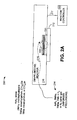
- FIG. 1A is a schematic view illustrating an exemplary vertical-cavity surface-emitting laser (VCSEL) 100 constructed in accordance with an aspect of the invention.
- the VCSEL 100 comprises an N-type gallium arsenide (GaAs) substrate 102 over which an N-type distributed Bragg reflector (DBR) 110 is formed.
- the DBR 110 includes approximately 40 alternating pairs of aluminum arsenide (AlAs) and gallium arsenide (GaAs) epitaxial layers, exemplary ones of which are illustrated using reference numerals 112 and 114, respectively.
- the reflectivity of the DBR 110 is determined by the index of refraction difference between the two materials that comprise the alternating layers of the DBR and the number of layers used to construct the DBR. These parameters, as well as others, can be varied to fabricate a DBR having specific properties.
- a gallium arsenide (GaAs) lower cavity spacer layer 120 is formed over the DBR 110.
- GaAs gallium arsenide
- a pair of cavity spacer layers sandwich the active region and are sometimes referred to as optical cavity spacer layers, or cavity spacer layers.
- the thickness of the cavity spacer layers is adjusted to optimize the optical mode and quantum well gain of the VCSEL, thereby providing the proper Fabry-Perot resonance, as known to those having ordinary skill in the art.
- An analogous structure is the separate confinement heterostructure (SCH) layers that sandwich the active region in an edge-emitting device.
- SCH separate confinement heterostructure
- an active region 130 comprising alternating layers of indium gallium arsenide nitride (InGaAsN) quantum well layers and GaAs barrier layers is then formed over the GaAs lower cavity spacer layer 120.
- a GaAs upper cavity spacer layer 140 is formed over the active region 130 and a p-type DBR 150 comprising approximately 25 alternating pairs of AlAs and GaAs epitaxial layers is formed over the GaAs upper cavity spacer layer 140.
- An InGaAsN quantum well layer and the surrounding GaAs barrier layers form a quantum well.
- the GaAs lower cavity spacer layer 120 forms the barrier layer for the lowermost InGaAsN quantum well layer in the active region 130.
- the GaAs upper cavity spacer layer 140 forms the barrier layer for the uppermost InGaAsN quantum well layer in the active region 130.
- the GaAs lower cavity spacer layer 120, the GaAs upper cavity spacer layer 140, and the active region 130 form an optical cavity 160 in which light generated by the active region 130 and reflected between the DBRs 110 and 150 passes until emitted through one of the DBRs.
- one of the DBRs will have a reflectivity slightly less than the other DBR. In this manner, light will be emitted from the VCSEL through the reflector having the slightly less reflectivity.
- InGaAsN quantum well layers that are formed as part of the active region 130 are grown in an OMVPE reactor at an elevated pressure, as will be described below with particular reference to FIG. 2.
- high quality InGaAsN quantum well layers are grown using a growth stop procedure in which epitaxial growth is stopped during the introduction of nitrogen. This "growth stop" procedure will be described in greater detail with respect to FIGS. 5A through 5F.
- FIG. 1B is a schematic view illustrating the optical cavity 160 of the VCSEL 100 of FIG. 1A.
- the active region 130 that includes a first InGaAsN quantum well layer 132 fabricated over the GaAs lower cavity spacer layer 120.
- a GaAs barrier layer 134 is fabricated over the first InGaAsN quantum well layer 132.
- the combination of an InGaAsN quantum well layer and the surrounding GaAs barrier layer 134 and GaAs lower cavity spacer layer 120 forms a quantum well. Alternating quantum well layers and barrier layers are deposited until the desired number of quantum wells is formed.
- the GaAs upper cavity spacer layer 140 is fabricated over the last InGaAsN quantum well layer, thus completing the optical cavity 160.
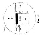
- FIG. 2A is a schematic diagram 200 illustrating an OMVPE reactor 210 constructed in accordance with an embodiment of the invention. Many of the details of an OMVPE reactor are omitted for clarity, as they are known to those having ordinary skill in the art.
- a reactor controller 215 is coupled to the reactor 210 via connection 217. The reactor controller can control various operating aspects and parameters of the reactor 210. As will be described in greater detail below, the reactor controller 215 can be used to control, among other parameters, the pressure in the reactor 210 during epitaxial growth.
- a carrier gas is bubbled through the constituent precursor compounds so that a saturated vaporous precursor is created for each compound.
- the saturated vaporous precursors are then diluted with other gasses as known to those having ordinary skill in the art.
- the vaporous precursors are transported into the reactor by the carrier gas.
- the vaporous precursors are pyrolized inside the reactor and passed over a heated substrate wafer, yielding the constituent atomic elements. These elements are deposited on the heated substrate wafer, where they bond to the underlying crystal structure of the substrate wafer, thereby forming an epitaxial layer.
- the vaporous precursors 214 may include arsine (AsH 3 ), the arsenic precursor, dimethylhydrazine (DMHy), the nitrogen precursor, trimethylgallium (TMGa), the gallium precursor, trimethylindium (TMIn), the indium precursor, and a carrier gas.
- Arsine Ar
- DHy dimethylhydrazine
- TMGa trimethylgallium
- TMIn trimethylindium
- TMIn trimethylindium
- the indium precursor and a carrier gas.
- Trimethylgallium is also known to those having ordinary skill in the art as alkyl-gallium, which has the chemical formula (CH 3 ) 3 Ga
- trimethylindium is also known to those having ordinary skill in the art as alkyl-indium, which has the chemical formula (CH 3 ) 3 In.
- vaporous precursors can also be used depending on the desired composition of the epitaxial layers.
- the carrier gas can be, for example, hydrogen (H 2 ) or nitrogen (N 2 ).
- the carrier gas is bubbled through these chemical precursors. These flows are subsequently combined into a vaporous mixture of the appropriate concentrations, and carried into the OMVPE reactor 210.
- a heated susceptor 212 comprises a heated surface (typically graphite, silicon carbide, or molybdenum) on which a crystalline substrate 220 resides.
- the DBR 110, lower cavity spacer layer 120, active region 130, upper cavity spacer layer 140 and the DBR 150 are grown over the crystalline substrate 220 and form the VCSEL 100 (FIG. 1A).
- the InGaAsN quantum well layers and GaAs barrier layers are grown over the lower cavity spacer layer 120 (FIG. 1B) as will be described below with respect to FIG. 2B.
- the substrate is GaAs to ensure lattice matched epitaxial growth of the GaAs lower and upper cavity spacer layers 120, 140, and the DBRs 110 and 150.
- the GaAs substrate ensures a lattice match for AlGaAs cladding layers.
- the InGaAsN material that forms the quantum well layers has a bulk lattice constant that is larger than the bulk lattice constant of the GaAs lower cavity spacer layer 120. Therefore the lattice mismatch that occurs between the InGaAsN material and the GaAs material subjects the InGaAsN layers to a compressive strain, referred to as biaxial compression.
- the vaporous precursors travel into the OMVPE reactor, as indicated using arrow 216, and eventually pass over the heated substrate 220.
- the vaporous precursors pass over the heated substrate 220, they are decomposed by pyrolysis and/or surface reactions, thereby releasing the constituent species on the substrate surface. These species settle on the heated surface of the substrate 220, where they bond to the underlying crystal structure. In this manner, epitaxial growth occurs in the OMVPE reactor 210.
- FIG. 2B is a detailed view of the VCSEL 100 shown in FIG. 2A partway through the fabrication process.
- the epitaxial layers that form the DBR 110, lower cavity spacer layer 120, active region 130, upper cavity spacer layer 140 and the DBR 150 are deposited using MOCVD.
- the pressure in the OMVPE reactor 210 is elevated so that the arsine flow rate can be reduced. This results in a larger proportion of nitrogen being extracted from the dimethylhydrazine and deposited in the InGaAsN quantum well layers.
- Typical growth pressure in an OMVPE reactor ranges from 50 to 100 millibar (mbar). However, the pressure in the OMVPE reactor 210 can be increased to several hundred mbar, even approaching atmospheric pressure (1000 mbar).
- Raising the pressure in the OMVPE reactor 210 permits continuous growth of InGaAsN while ensuring that a sufficient quantity of nitrogen is deposited on the epitaxial layer. Raising the pressure in the OMVPE reactor 210 reduces the amount of arsine (AsH 3 ) required to produce a high quality optical device. The reduced arsine requirement permits a relatively high dimethylhydrazine (DMHy) ratio, thereby reducing the likelihood that the arsenic will occupy the group-V lattice sites that are preferably left vacant for the nitrogen to occupy.
- DMHy dimethylhydrazine
- a first InGaAsN quantum well layer 224 is grown over the GaAs lower cavity spacer layer 120. Because the lower cavity spacer layer 120 is formed using GaAs, the lower cavity spacer layer 120 acts as a barrier layer for the first InGaAs quantum well layer 224. A GaAs barrier layer 226 is then grown over the first InGaAsN quantum well layer 224. This growth process is repeated until the desired number of quantum wells is grown.
- the arsine partial pressure is a growth parameter that is frequently expressed as the V:III ratio, which is directly proportional to the arsine partial pressure for GaAs. This analysis can easily be extended to quaternary compounds such as InGaAsN, as will be described below.
- the poor optoelectronic quality of GaAs grown with an insufficient V:III ratio suggests that some minimum partial pressure of arsine is desirable to suppress the formation of defects that limit the light-emission efficiency of the device. These defects may be arsenic vacancies, which are more likely to form under arsenic-deficient conditions. Regarding the solid-state chemistry of defect formation, the group-V vacancy concentration tends to diminish as the concentration of active group-V precursor species in the vapor over the substrate wafer is raised. Thus, there is some threshold value for the arsine partial pressure for producing material of good optical quality.
- an arsine partial pressure of at least 1 mbar provides material having excellent optoelectronic characteristics, which can be characterized by an internal quantum efficiency of radiative recombination approaching 100%.
- the minimum partial pressure of arsine (AsH 3 ) may be obtained with a decreased arsine flow rate.
- a typical single-wafer reactor may have a carrier flow rate of several liters per minute. If growth is conducted at a low pressure of 50 mbar, an arsine flow rate of about 50 standard cubic centimeters per minute (sccm) is preferable for growth of material having excellent optoelectronic characteristics. This flow rate establishes an arsine (AsH 3 ) partial pressure estimated to be ⁇ 1 mbar.
- the arsine partial pressure requirement can be satisfied by a flow rate decreased to only about 10 sccm.
- This lower arsine flow rate during OMVPE growth at higher pressures applies to other reactor geometries as well.
- an arsine flow rate of only approximately 20 sccm is desired for growth at atmospheric pressure, while 100 sccm is desired at 100mbar (both corresponding to an arsine partial pressure of about 1-2 mbar).
- a primary challenge in InGaAsN growth is realizing a very high vapor concentration of the exemplary nitrogen precursor dimethylhydrazine, while still preserving an arsine partial pressure that is sufficient for growth of material having an internal quantum efficiency of radiative recombination approaching 100%.
- the [N] vapor composition can conventionally be increased by reducing the arsine flow rate, this may also produce material having poor optoelectronic characteristics.
- the arsine flow rate may be reduced, while maintaining the same arsine partial pressure.
- the resulting mixture is highly nitrogen-rich for enhancing the nitrogen content of InGaAsN alloys, and forming a material having excellent optoelectronic characteristics.
- the advantage for a lower arsine (AsH 3 ) flow rate is especially clear when it is considered that the dimethylhydrazine flow rate is limited because it is a liquid source, the vapor of which is transported into the reactor using a carrier gas, such as hydrogen.
- a carrier gas such as hydrogen.
- the bubbler's carrier gas flow should not exceed 500 sccm. Otherwise, the carrier gas may no longer be saturated with the precursor vapor.
- the bubbler temperature should be held lower than room temperature to avoid condensation in the gas lines between the bubbler and reactor.
- the nitrogen content of the InGaAsN film will increase as the nitrogen content of the vapor increases.
- the maximum DMHy bubbler flow rate should be used, along with an arsine flow rate no higher than that, which satisfies the arsine partial pressure requirement.
- this example indicates that raised growth pressure can enable a significantly higher nitrogen concentration in the vapor, while simultaneously maintaining sufficient arsine supply for epitaxial growth of material with excellent optoelectronic quality.
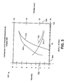
- FIG. 3 is a graphical illustration 300 showing a comparison of the photoluminescence for two InGaAs quantum wells, one fabricated at an increased growth pressure of 100 mbar and the other fabricated at an increased growth pressure of 200 mbar.
- InGaAs quantum wells are used to illustrate the minimum amount of arsine used to grow an InGaAs quantum well having high optical quality.
- FIG. 3 illustrates the effect that increasing the total growth pressure and lowering the arsine flow rate has on light intensity.
- the left-hand vertical axis 302 represents light intensity
- the righthand vertical axis 306 represents the full width at half maximum (FWHM) spectral peak in millielectron volts (meV)
- the horizontal axis 304 represents the arsine (AsH 3 ) to group-III material ratio.
- This ratio represents the absolute ratio of arsine (AsH 3 ) to group-III materials.
- an arsine (AsH 3 ) to group-III ratio of 10 indicates that atomically there are 10 times more arsine (AsH 3 ) molecules than group-III precursor molecules.
- This ratio is also the arsine to group III atomic ratio because each arsine molecule contains one arsenic atom and the TMGa and TMIn molecules each contribute one group III atom.
- the indium and gallium are considered the group-III materials, while arsenic is the group-V material.
- the intensity of the phosphorescence of the InGaAs quantum well represented by curve 310 exceeds the intensity of the phosphorescence of the InGaAs quantum well represented by curve 312, which was grown at a 100 mbar growth pressure, for arsine (AsH 3 ) to group III ratios in the approximate range of 2-80.
- the arsine to group-III ratio indicates a lower arsine quantity for a given intensity and FWHM value for the InGaAs quantum well fabricated at the elevated 200 mbar growth pressure.
- the width of the spectral peak of the InGaAs quantum well formed at a growth pressure of 200 mbar is narrower than the width of the spectral peak of the InGaAs quantum well formed at a growth pressure of 100 mbar, referred to using reference numeral 316. From the graph 300 it is clear that a high quality InGaAs quantum well can be grown with a lower arsine to group-III ratio, and therefore, at a lower arsine flow rate, by raising the reactor pressure from 100 mbar to 200 mbar.
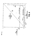
- FIG. 4 is a graphical illustration 400 showing the relationship between the concentration of nitrogen (N) in an epitaxial layer (y in InGaAs 1-y N y ) and the concentration of nitrogen precursor in the vapor (DMHy / [DMHy + AsH 3 ]).
- the vertical axis 402 represents the fraction of nitrogen in an epitaxial layer of InGaAsN
- the horizontal axis 404 represents the concentration of nitrogen precursor in the vapor DMHy / [DMHy + AsH 3 ] (the total group-V precursor including the arsine and the DMHy).
- the dotted diagonal line 406 represents a nitrogen incorporation of unity in the epitaxial layer for dimethylhydrazine.
- the amount of nitrogen in the solid epitaxial film (the vertical axis 402) at a growth pressure of 200 mbar far exceeds the amount of nitrogen in the solid film at a growth pressure of 50 mbar.
- a higher growth pressure permits a higher [N] solid because the arsine content (AsH 3 ), as a proportion of the total group-V material, may be reduced so that the InGaAsN film may be grown in a more nitrogen-rich environment.
- FIGS. 5A through 5F are schematic views illustrating an alternative embodiment of the invention.
- one or more sublayers of InGaAs 504 are formed over a GaAs region, which has the same characteristics as the GaAs lower cavity spacer layer 120 described above.
- the sublayers each have a thickness of one or two atoms.
- the growth of the InGaAs sublayer 504 is stopped. This is referred to as a "growth stop" where the flow of the group-III precursors is discontinued. Additionally, the arsine flow rate is lowered and a high DMHy flow rate is switched into the reactor. This exposes the surface of the sublayer 504 to an ambient atmosphere with a very high nitrogen vapor content.
- the nitrogen atoms an exemplary one of which is indicated using reference numeral 506, bond to and are incorporated in the sublayer 504.
- FIG. 5C the flow of the DMHy is discontinued, the flow of the group-III precursors is restored and the arsine flow is restored to its original level. Accordingly, the growth of the InGaAs is resumed and an additional sublayer 508 comprising InGaAs is grown over the nitrogen atoms 506.
- FIG. 5D another growth stop is performed, and the surface of the sublayer 508 is exposed to an ambient atmosphere having a very high nitrogen vapor content.
- nitrogen atoms 510 bond to the surface of the sublayer 508.
- a typical quantum well layer has a thickness of eight (8) nm, which, for InGaAsN are 15 sublayers.
- each InGaAsN quantum well layer comprises eight (8) growth stop/nitrogen dose cycles, although more or fewer growth stop/nitrogen dose cycles are possible.
- FIG. 5E alternating growth of InGaAs sublayers and nitrogen dosing steps is continued until a full thickness quantum well layer 520 of InGaAsN is grown.
- a barrier layer 522 of, for example, GaAs is grown over the InGaAsN quantum well layer 520. In this manner, InGaAsN having higher average nitrogen content may be achieved.
- FIGS. 5A through 5F demonstrate that a high nitrogen content may be incorporated into an InGaAsN epitaxial film at an interface during a growth stop with a dimethylhydrazine + arsine mixture flowing into the reactor.
- analysis indicates a very high nitrogen content at the first QW interface (nitrogen atoms 506), when a 5-sec growth stop is incorporated to establish AsH 3 and DMHy flows into the reactor.
- nitrogen atoms 506 nitrogen atoms 506
- an InGaAs sublayer by growing one monolayer of GaAs by discontinuing the indium precursor during growth of the monolayer.
- Such a monolayer could be formed by using a composition of In x GaAs 1-x , where x is equal to 0.
- the resultant GaAs surface is then exposed to a mixture of DMHy and AsH 3 that is rich in DMHy to enhance the nitrogen content in the InGaAsN.
- the arsine flow rate should be somewhat less than the flow rate required to support growth of high-quality material. Consequently, during each growth stop, the arsine flow rate may be reduced, thereby increasing the relative DMHy content of the vapor mixture to further encourage greater nitrogen incorporation.
Landscapes
- Chemical & Material Sciences (AREA)
- Engineering & Computer Science (AREA)
- Materials Engineering (AREA)
- Metallurgy (AREA)
- Organic Chemistry (AREA)
- Crystallography & Structural Chemistry (AREA)
- Condensed Matter Physics & Semiconductors (AREA)
- Physics & Mathematics (AREA)
- General Physics & Mathematics (AREA)
- Manufacturing & Machinery (AREA)
- Computer Hardware Design (AREA)
- Microelectronics & Electronic Packaging (AREA)
- Power Engineering (AREA)
- General Chemical & Material Sciences (AREA)
- Inorganic Chemistry (AREA)
- Chemical Kinetics & Catalysis (AREA)
- Semiconductor Lasers (AREA)
- Crystals, And After-Treatments Of Crystals (AREA)
Applications Claiming Priority (2)
| Application Number | Priority Date | Filing Date | Title |
|---|---|---|---|
| US140625 | 2002-05-07 | ||
| US10/140,625 US6756325B2 (en) | 2002-05-07 | 2002-05-07 | Method for producing a long wavelength indium gallium arsenide nitride(InGaAsN) active region |
Publications (2)
| Publication Number | Publication Date |
|---|---|
| EP1361601A2 true EP1361601A2 (de) | 2003-11-12 |
| EP1361601A3 EP1361601A3 (de) | 2005-07-27 |
Family
ID=29249790
Family Applications (1)
| Application Number | Title | Priority Date | Filing Date |
|---|---|---|---|
| EP03001970A Withdrawn EP1361601A3 (de) | 2002-05-07 | 2003-01-30 | Verfahren zur Herstellung eines langwelligen Indium-Gallium-Arsenid-Nitrid (InGaAsN) aktiven Bereichs |
Country Status (3)
| Country | Link |
|---|---|
| US (2) | US6756325B2 (de) |
| EP (1) | EP1361601A3 (de) |
| JP (1) | JP2003332696A (de) |
Cited By (2)
| Publication number | Priority date | Publication date | Assignee | Title |
|---|---|---|---|---|
| EP4261323A1 (de) * | 2022-04-11 | 2023-10-18 | IQE plc | Verfahren und system für ein gemischtes gruppe-v-vorläuferverfahren |
| WO2025067786A1 (en) * | 2023-09-27 | 2025-04-03 | Iqe Plc | Semiconductor structures |
Families Citing this family (33)
| Publication number | Priority date | Publication date | Assignee | Title |
|---|---|---|---|---|
| US6697404B1 (en) * | 1996-08-30 | 2004-02-24 | Ricoh Company, Ltd. | Laser diode operable in 1.3μm or 1.5μm wavelength band with improved efficiency |
| US20030219917A1 (en) * | 1998-12-21 | 2003-11-27 | Johnson Ralph H. | System and method using migration enhanced epitaxy for flattening active layers and the mechanical stabilization of quantum wells associated with vertical cavity surface emitting lasers |
| US6674785B2 (en) * | 2000-09-21 | 2004-01-06 | Ricoh Company, Ltd. | Vertical-cavity, surface-emission type laser diode and fabrication process thereof |
| US20040161006A1 (en) * | 2003-02-18 | 2004-08-19 | Ying-Lan Chang | Method and apparatus for improving wavelength stability for InGaAsN devices |
| US7860137B2 (en) | 2004-10-01 | 2010-12-28 | Finisar Corporation | Vertical cavity surface emitting laser with undoped top mirror |
| CN101432936B (zh) | 2004-10-01 | 2011-02-02 | 菲尼萨公司 | 具有多顶侧接触的垂直腔面发射激光器 |
| JP4925601B2 (ja) | 2005-04-18 | 2012-05-09 | 三菱電機株式会社 | 半導体装置 |
| US7843982B2 (en) * | 2005-12-15 | 2010-11-30 | Palo Alto Research Center Incorporated | High power semiconductor device to output light with low-absorbtive facet window |
| US7764721B2 (en) * | 2005-12-15 | 2010-07-27 | Palo Alto Research Center Incorporated | System for adjusting the wavelength light output of a semiconductor device using hydrogenation |
| US7526007B2 (en) * | 2005-12-15 | 2009-04-28 | Palo Alto Research Center Incorporated | Buried lateral index guided lasers and lasers with lateral current blocking layers |
| US20070153851A1 (en) * | 2005-12-15 | 2007-07-05 | Palo Alto Research Center Incorporated | On-chip integration of passive and active optical components enabled by hydrogenation |
| WO2009009111A2 (en) * | 2007-07-10 | 2009-01-15 | The Board Of Trustees Of The Leland Stanford Junior University | GaInNAsSB SOLAR CELLS GROWN BY MOLECULAR BEAM EPITAXY |
| US20100006023A1 (en) * | 2008-07-11 | 2010-01-14 | Palo Alto Research Center Incorporated | Method For Preparing Films And Devices Under High Nitrogen Chemical Potential |
| US20100319764A1 (en) * | 2009-06-23 | 2010-12-23 | Solar Junction Corp. | Functional Integration Of Dilute Nitrides Into High Efficiency III-V Solar Cells |
| US20110114163A1 (en) * | 2009-11-18 | 2011-05-19 | Solar Junction Corporation | Multijunction solar cells formed on n-doped substrates |
| US20110232730A1 (en) * | 2010-03-29 | 2011-09-29 | Solar Junction Corp. | Lattice matchable alloy for solar cells |
| US9214580B2 (en) | 2010-10-28 | 2015-12-15 | Solar Junction Corporation | Multi-junction solar cell with dilute nitride sub-cell having graded doping |
| US20150221803A1 (en) | 2014-02-05 | 2015-08-06 | Solar Junction Corporation | Monolithic multijunction power converter |
| US8962991B2 (en) | 2011-02-25 | 2015-02-24 | Solar Junction Corporation | Pseudomorphic window layer for multijunction solar cells |
| US8927066B2 (en) * | 2011-04-29 | 2015-01-06 | Applied Materials, Inc. | Method and apparatus for gas delivery |
| US8766087B2 (en) | 2011-05-10 | 2014-07-01 | Solar Junction Corporation | Window structure for solar cell |
| US9159873B2 (en) | 2011-11-14 | 2015-10-13 | Quantum Electro Opto Systems Sdn. Bhd. | High speed optical tilted charge devices and methods |
| CN103930994A (zh) * | 2011-11-14 | 2014-07-16 | 量子电镀光学系统有限公司 | 光学倾斜电荷装置及方法 |
| WO2013074530A2 (en) | 2011-11-15 | 2013-05-23 | Solar Junction Corporation | High efficiency multijunction solar cells |
| US9153724B2 (en) | 2012-04-09 | 2015-10-06 | Solar Junction Corporation | Reverse heterojunctions for solar cells |
| US8860005B1 (en) * | 2013-08-08 | 2014-10-14 | International Business Machines Corporation | Thin light emitting diode and fabrication method |
| DE102013225632A1 (de) * | 2013-12-11 | 2015-06-11 | Fraunhofer-Gesellschaft zur Förderung der angewandten Forschung e.V. | Verfahren zur Herstellung einer Schicht |
| US9865769B2 (en) | 2015-03-23 | 2018-01-09 | International Business Machines Corporation | Back contact LED through spalling |
| US20170110613A1 (en) | 2015-10-19 | 2017-04-20 | Solar Junction Corporation | High efficiency multijunction photovoltaic cells |
| US10957818B2 (en) | 2016-09-30 | 2021-03-23 | Intel Corporation | High performance light emitting diode and monolithic multi-color pixel |
| WO2019010037A1 (en) | 2017-07-06 | 2019-01-10 | Solar Junction Corporation | HYBRID MOCVD / MBE EPITAXIAL GROWTH OF MULTI-JUNCTION SOLAR CELLS ADAPTED TO THE HIGH-PERFORMANCE NETWORK |
| WO2019067553A1 (en) | 2017-09-27 | 2019-04-04 | Solar Junction Corporation | SHORT-LENGTH WAVELENGTH INFRARED OPTOELECTRONIC DEVICES HAVING DILUTED NITRIDE LAYER |
| US11211514B2 (en) | 2019-03-11 | 2021-12-28 | Array Photonics, Inc. | Short wavelength infrared optoelectronic devices having graded or stepped dilute nitride active regions |
Family Cites Families (12)
| Publication number | Priority date | Publication date | Assignee | Title |
|---|---|---|---|---|
| JP3445653B2 (ja) * | 1994-03-23 | 2003-09-08 | 士郎 酒井 | 発光素子 |
| JP2917913B2 (ja) * | 1996-06-10 | 1999-07-12 | 日本電気株式会社 | 半導体光素子の製造方法 |
| US6233264B1 (en) * | 1996-08-27 | 2001-05-15 | Ricoh Company, Ltd. | Optical semiconductor device having an active layer containing N |
| US5719895A (en) * | 1996-09-25 | 1998-02-17 | Picolight Incorporated | Extended wavelength strained layer lasers having short period superlattices |
| US6764928B1 (en) * | 1997-02-20 | 2004-07-20 | Semiconductor Energy Laboratory Co., Ltd. | Method of manufacturing an El display device |
| JP3683669B2 (ja) * | 1997-03-21 | 2005-08-17 | 株式会社リコー | 半導体発光素子 |
| WO1998044539A1 (en) * | 1997-03-28 | 1998-10-08 | Sharp Kabushiki Kaisha | Method for manufacturing compound semiconductors |
| JPH1174485A (ja) * | 1997-06-30 | 1999-03-16 | Toshiba Corp | 半導体装置およびその製造方法 |
| US5944913A (en) * | 1997-11-26 | 1999-08-31 | Sandia Corporation | High-efficiency solar cell and method for fabrication |
| US6150677A (en) * | 1998-02-19 | 2000-11-21 | Sumitomo Electric Industries, Ltd. | Method of crystal growth of compound semiconductor, compound semiconductor device and method of manufacturing the device |
| US6207973B1 (en) * | 1998-08-19 | 2001-03-27 | Ricoh Company, Ltd. | Light emitting devices with layered III-V semiconductor structures |
| US6764926B2 (en) * | 2002-03-25 | 2004-07-20 | Agilent Technologies, Inc. | Method for obtaining high quality InGaAsN semiconductor devices |
-
2002
- 2002-05-07 US US10/140,625 patent/US6756325B2/en not_active Expired - Lifetime
-
2003
- 2003-01-30 EP EP03001970A patent/EP1361601A3/de not_active Withdrawn
- 2003-05-07 JP JP2003129259A patent/JP2003332696A/ja not_active Withdrawn
-
2004
- 2004-02-23 US US10/785,747 patent/US7033938B2/en not_active Expired - Fee Related
Cited By (3)
| Publication number | Priority date | Publication date | Assignee | Title |
|---|---|---|---|---|
| EP4261323A1 (de) * | 2022-04-11 | 2023-10-18 | IQE plc | Verfahren und system für ein gemischtes gruppe-v-vorläuferverfahren |
| US12518962B2 (en) | 2022-04-11 | 2026-01-06 | Iqe Plc | Method and system for mixed group V precursor process |
| WO2025067786A1 (en) * | 2023-09-27 | 2025-04-03 | Iqe Plc | Semiconductor structures |
Also Published As
| Publication number | Publication date |
|---|---|
| US20040219703A1 (en) | 2004-11-04 |
| US6756325B2 (en) | 2004-06-29 |
| JP2003332696A (ja) | 2003-11-21 |
| US20030211647A1 (en) | 2003-11-13 |
| EP1361601A3 (de) | 2005-07-27 |
| US7033938B2 (en) | 2006-04-25 |
Similar Documents
| Publication | Publication Date | Title |
|---|---|---|
| US6756325B2 (en) | Method for producing a long wavelength indium gallium arsenide nitride(InGaAsN) active region | |
| Ustinov et al. | GaAs-based long-wavelength lasers | |
| US6934312B2 (en) | System and method for fabricating efficient semiconductor lasers via use of precursors having a direct bond between a group III atom and a nitrogen atom | |
| JP4259709B2 (ja) | 量子井戸型活性層 | |
| US20080137701A1 (en) | Gallium Nitride Based Semiconductor Device with Reduced Stress Electron Blocking Layer | |
| US20040161006A1 (en) | Method and apparatus for improving wavelength stability for InGaAsN devices | |
| US5547898A (en) | Method for p-doping of a light-emitting device | |
| EP2403023A1 (de) | Verfahren zur herstellung eines lichtemittierenden elements und lichtemittierendes element | |
| US6108360A (en) | Long wavelength DH, SCH and MQW lasers based on Sb | |
| WO2007136385A1 (en) | Gallium nitride based semiconductor device with electron blocking layer | |
| US7915634B2 (en) | Laser diode epitaxial wafer and method for producing same | |
| US6887727B2 (en) | System and method for increasing nitrogen incorporation into a semiconductor material layer using an additional element | |
| US6750120B1 (en) | Method and apparatus for MOCVD growth of compounds including GaAsN alloys using an ammonia precursor with a catalyst | |
| US5762705A (en) | Fabrication method of semiconductor laser by MOVPE | |
| JP3654331B2 (ja) | 半導体製造方法および半導体発光素子 | |
| JP4006055B2 (ja) | 化合物半導体の製造方法及び化合物半導体装置 | |
| US6821806B1 (en) | Method for forming compound semiconductor layer and compound semiconductor apparatus | |
| US20090309189A1 (en) | Method for the growth of indium nitride | |
| US20070241322A1 (en) | Long Wavelength Induim Arsenide Phosphide (InAsP) Quantum Well Active Region And Method For Producing Same | |
| RU2836258C1 (ru) | Способ изготовления гетероструктуры полупроводникового лазера ближнего инфракрасного диапазона с безалюминиевой активной областью | |
| JP4450269B2 (ja) | 半導体発光素子の製造方法 | |
| JP3772794B2 (ja) | 化合物半導体の製造方法 | |
| JP2004288789A (ja) | 面発光型半導体レーザ素子の製造方法および結晶成長装置、ならびにこれらを用いて形成した面発光型半導体レーザ素子、該面発光型半導体レーザ素子を用いた光送信モジュール、光送受信モジュール、光通信システム | |
| US20040115854A1 (en) | Method of MOCVD growth of compounds including GaAsN alloys using an ammonia precursor and radiation | |
| Padullaparthi | Appendix B: Epitaxial Growth Engineering |
Legal Events
| Date | Code | Title | Description |
|---|---|---|---|
| PUAI | Public reference made under article 153(3) epc to a published international application that has entered the european phase |
Free format text: ORIGINAL CODE: 0009012 |
|
| AK | Designated contracting states |
Kind code of ref document: A2 Designated state(s): AT BE BG CH CY CZ DE DK EE ES FI FR GB GR HU IE IT LI LU MC NL PT SE SI SK TR |
|
| AX | Request for extension of the european patent |
Extension state: AL LT LV MK RO |
|
| PUAL | Search report despatched |
Free format text: ORIGINAL CODE: 0009013 |
|
| AK | Designated contracting states |
Kind code of ref document: A3 Designated state(s): AT BE BG CH CY CZ DE DK EE ES FI FR GB GR HU IE IT LI LU MC NL PT SE SI SK TR |
|
| AX | Request for extension of the european patent |
Extension state: AL LT LV MK RO |
|
| RIC1 | Information provided on ipc code assigned before grant |
Ipc: 7H 01S 5/343 B Ipc: 7H 01S 5/323 B Ipc: 7C 30B 25/02 B Ipc: 7C 30B 29/40 B Ipc: 7C 30B 29/38 B Ipc: 7H 01L 21/205 A |
|
| 17P | Request for examination filed |
Effective date: 20051214 |
|
| AKX | Designation fees paid |
Designated state(s): DE FR GB |
|
| RAP1 | Party data changed (applicant data changed or rights of an application transferred) |
Owner name: AVAGO TECHNOLOGIES ECBU IP (SINGAPORE) PTE. LTD. |
|
| STAA | Information on the status of an ep patent application or granted ep patent |
Free format text: STATUS: THE APPLICATION IS DEEMED TO BE WITHDRAWN |
|
| 18D | Application deemed to be withdrawn |
Effective date: 20110802 |