EP1358502B1 - Gmr-struktur und verfahren zu deren herstellung - Google Patents
Gmr-struktur und verfahren zu deren herstellung Download PDFInfo
- Publication number
- EP1358502B1 EP1358502B1 EP02701230A EP02701230A EP1358502B1 EP 1358502 B1 EP1358502 B1 EP 1358502B1 EP 02701230 A EP02701230 A EP 02701230A EP 02701230 A EP02701230 A EP 02701230A EP 1358502 B1 EP1358502 B1 EP 1358502B1
- Authority
- EP
- European Patent Office
- Prior art keywords
- layer
- gmr
- insulation layer
- multiple layer
- metallic
- Prior art date
- Legal status (The legal status is an assumption and is not a legal conclusion. Google has not performed a legal analysis and makes no representation as to the accuracy of the status listed.)
- Expired - Lifetime
Links
- 238000000034 method Methods 0.000 title claims abstract description 43
- 238000004519 manufacturing process Methods 0.000 title claims abstract description 27
- 239000002184 metal Substances 0.000 claims abstract description 20
- 229910052751 metal Inorganic materials 0.000 claims abstract description 20
- 238000002161 passivation Methods 0.000 claims description 32
- 239000000758 substrate Substances 0.000 claims description 28
- 238000009413 insulation Methods 0.000 claims description 25
- 239000004065 semiconductor Substances 0.000 claims description 20
- 238000000151 deposition Methods 0.000 claims description 10
- 238000005498 polishing Methods 0.000 claims description 10
- 238000000059 patterning Methods 0.000 claims description 9
- 230000008021 deposition Effects 0.000 claims description 7
- 239000000126 substance Substances 0.000 claims description 7
- 238000006073 displacement reaction Methods 0.000 claims description 3
- XUIMIQQOPSSXEZ-UHFFFAOYSA-N Silicon Chemical compound [Si] XUIMIQQOPSSXEZ-UHFFFAOYSA-N 0.000 description 8
- 229910052710 silicon Inorganic materials 0.000 description 8
- 239000010703 silicon Substances 0.000 description 8
- 230000000694 effects Effects 0.000 description 6
- 238000001312 dry etching Methods 0.000 description 5
- 238000011156 evaluation Methods 0.000 description 5
- 238000001459 lithography Methods 0.000 description 3
- 230000005415 magnetization Effects 0.000 description 3
- VYPSYNLAJGMNEJ-UHFFFAOYSA-N Silicium dioxide Chemical compound O=[Si]=O VYPSYNLAJGMNEJ-UHFFFAOYSA-N 0.000 description 2
- 238000005530 etching Methods 0.000 description 2
- 238000010884 ion-beam technique Methods 0.000 description 2
- 239000000463 material Substances 0.000 description 2
- 235000012431 wafers Nutrition 0.000 description 2
- 229910000604 Ferrochrome Inorganic materials 0.000 description 1
- 230000005355 Hall effect Effects 0.000 description 1
- 229910052581 Si3N4 Inorganic materials 0.000 description 1
- 229910004298 SiO 2 Inorganic materials 0.000 description 1
- 238000011109 contamination Methods 0.000 description 1
- 238000012864 cross contamination Methods 0.000 description 1
- 238000005137 deposition process Methods 0.000 description 1
- 238000005516 engineering process Methods 0.000 description 1
- 238000001755 magnetron sputter deposition Methods 0.000 description 1
- 230000000873 masking effect Effects 0.000 description 1
- 238000005259 measurement Methods 0.000 description 1
- 238000001465 metallisation Methods 0.000 description 1
- 150000002739 metals Chemical class 0.000 description 1
- 238000000206 photolithography Methods 0.000 description 1
- 238000000623 plasma-assisted chemical vapour deposition Methods 0.000 description 1
- 238000001552 radio frequency sputter deposition Methods 0.000 description 1
- 230000035945 sensitivity Effects 0.000 description 1
- 235000012239 silicon dioxide Nutrition 0.000 description 1
- 239000000377 silicon dioxide Substances 0.000 description 1
- HQVNEWCFYHHQES-UHFFFAOYSA-N silicon nitride Chemical compound N12[Si]34N5[Si]62N3[Si]51N64 HQVNEWCFYHHQES-UHFFFAOYSA-N 0.000 description 1
Images


Classifications
-
- G—PHYSICS
- G01—MEASURING; TESTING
- G01R—MEASURING ELECTRIC VARIABLES; MEASURING MAGNETIC VARIABLES
- G01R33/00—Arrangements or instruments for measuring magnetic variables
- G01R33/02—Measuring direction or magnitude of magnetic fields or magnetic flux
- G01R33/06—Measuring direction or magnitude of magnetic fields or magnetic flux using galvano-magnetic devices
- G01R33/09—Magnetoresistive devices
- G01R33/093—Magnetoresistive devices using multilayer structures, e.g. giant magnetoresistance sensors
-
- B—PERFORMING OPERATIONS; TRANSPORTING
- B82—NANOTECHNOLOGY
- B82Y—SPECIFIC USES OR APPLICATIONS OF NANOSTRUCTURES; MEASUREMENT OR ANALYSIS OF NANOSTRUCTURES; MANUFACTURE OR TREATMENT OF NANOSTRUCTURES
- B82Y25/00—Nanomagnetism, e.g. magnetoimpedance, anisotropic magnetoresistance, giant magnetoresistance or tunneling magnetoresistance
Definitions
- the invention relates to a method for producing a GMR structure ("giant magneto-resistance structure"), at the on a support a metallic multilayer is applied and in which the metallic multilayer to structure the GMR structure.
- the invention further relates to a GMR structure with a Carrier and arranged on the carrier structured metallic multilayer.
- Displacement and angle sensors that work on a magnetic basis, find, for example, in automotive technology numerous applications. Special advantages lie in that the sensors are contactless and therefore without mechanical Wear work. They are robust opposite Dirt, and they withstand high temperatures. Conventional magnetic sensors are based, for example the Hall effect or an AMR effect (anisotropic magneto-resistance effect).
- Such a Wheatstone bridge circuit can, for example contain four GMR elements.
- Prior art method for producing GMR elements are based on the deposition of magnetic and non-magnetic multilayers on an insulating Underground. After the metal deposition takes place Structuring of the metal level typically by means of Dry. As such a dry etching process For example, ion beam etching IBE ("Ion Beam etching "), an RF sputtering process or the lift-off technique at. The following are the electrical contacts mounted on the GMR element. Thereupon become Passivation layers deposited.
- the present invention relates to a method of manufacturing a GMR structure according to claim 1, a GMR structure according to claim 10 and the use of a GMR structure according to claim 13.
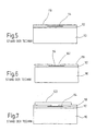
- Figures 1 to 7 illustrate a method of Prior art for producing a GMR structure. It are each intermediate states during the procedure in a sectional view through a layer arrangement shown.
- FIG. 1 shows a semiconductor substrate 110, for example Silicon, with an overlying insulation layer 112th
- FIG 2 shows the arrangement of Figure 1 with an additional on the insulating layer 112 applied metallic Multilayer 114.
- This metallic multilayer 114 which one according to their later function may also refer to GMR layer, for example applied by a deposition process.
- GMR layer for example applied by a deposition process.
- the GMR layer consists, for example, of Co / Craction FeCr / Cu layers. She typically has a total thickness of about 100 nm.
- Figure 4 a state is shown, which on the Build state according to Figure 3, and in which the GMR layer 114 is already structured. This can be, for example by dry etching, such as with IBE, be done. Further the resist mask 160 according to FIG. 3 was removed.
- a passivation layer 118 This can, for example, silicon dioxide, silicon nitride and comparable materials.
- FIG. 6 shows a state which is based on FIG The layer arrangement shown here is the passivation layer 118 structured, leaving a contact hole 162 is created.
- a state is then shown, which consists of the state of Figure 6 shows by a contact metal 122 is deposited.
- the invention is based on the generic method in that the carrier before the application of the metallic multilayer has a structure and that the structuring of the metallic multilayer by chemical-mechanical polishing (CMP, "chemical mechanical polishing") takes place.
- CMP chemical-mechanical polishing
- the structure of the GMR layers for example a typical meandering structure, is therefore predetermined at least partially by the structuring of the substrate or of the insulating layer arranged on the substrate, for example SiO 2 , even before the metallic multilayer is applied.
- the metal layers are removed by CMP again. In the depressions, however, the GMR structures are not removed. Structuring the GMR layer by lithography and costly dry etching processes are therefore unnecessary.
- the structured support is through Patterning of a semiconductor substrate and the following Depositing an insulation layer is generated.
- the depressions, which ultimately determine the GMR structure Thus, for example, by dry etching in a silicon substrate are introduced.
- the structure then remains after the deposition of an insulation layer, for example, based on a 0.5 to 1.5 microns thick thermal oxide obtained.
- Passivation layer may be the first passivation layer which is deposited during the process. It but can also be useful, this passivation layer to deposit, if already before structuring the metallic Multiple layer deposited a passivation layer has been.
- this passivation layer to deposit, if already before structuring the metallic Multiple layer deposited a passivation layer has been.
- the first passivation layer that is, after the Structuring the metallic multilayer deposited Passivation layer is the first passivation layer, already covers the passivation layer structured GMR layer.
- already before structuring the metallic multilayer a passivation layer has been deposited serves the after structuring the metallic multilayer deposited passivation layer to cover more open Flanks of the GMR layer.
- the method according to the invention is particularly advantageous further developed by the fact that after structuring the metallic multilayer deposited by CMP Passivation layer is structured and that below a contact metal is deposited. In this way becomes an electrical connection of the GMR structure to others Components possible.
- the structuring of the semiconductor substrate in the context of Structuring an integrated circuit on the same Semiconductor substrate is done.
- the definition of the GMR structure can thus be part of the structuring of the Semiconductor substrate used for integrated circuits become part of, for example, CMOS structures the evaluation circuit of the GMR structures.
- the method is particularly advantageously developed by rouge metallic multilayer in a first Area is applied, in which the GMR structure should be generated and that the metallic Multilayer applied in a second area becomes, in which structures for an integrated circuit available.
- the metallic multilayer in areas outside the GMR structure Wells removed by chemical mechanical polishing It is possible, the metallic multilayer unspecific on the entire surface of a To apply wafers. This eliminates masking steps.
- a further advantageous embodiment of the method is that before depositing the insulation layer a further insulation layer is applied, that applied to the further insulating layer, a layer which is at least one conductive connection between the first area and the second area to Provides, and that after the deposition of the insulating layer the insulation layer in the first area is structured so that the subsequently applied metallic multilayer an electrical contact to which has at least one electrical connection.
- a rational process becomes an electric one Connection between, for example, a CMOS structure and the GMR structure.
- the senior Connection between the GMR structure and the CMOS structure then lies below the GMR structure.
- the insulation layer in one first area is applied, in which the GMR structure should be generated, that the metallic multilayer is applied in a second area, in which structures are present for an integrated circuit and that the insulating layer in the second area acts as a passivation layer.
- the insulation layer in the first area is the insulation layer thus the carrier for the GMR structure.
- the second area covers the insulation layer the CMOS structure as a passivation layer.
- the invention is based on the generic GMR structure due to the fact that the structured metallic multilayer in one or more wells of the carrier is arranged.
- the structured Multiple layer in depressions it is possible, the Structuring of the multilayer by chemical-mechanical To produce polishing. Thus, it is not necessary to use complex structuring method.
- the carrier comprises a semiconductor substrate and an insulation layer.
- the depression can therefore so be introduced into the carrier that initially a recess is introduced into the semiconductor substrate and then an insulating layer on the semiconductor substrate is applied.
- the structured Multilayer becomes this way during the Protected manufacturing process.
- the GMR structure is advantageously developed by that on the semiconductor substrate an integrated Circuit is provided that between the integrated Circuit and the metallic multilayer at least one conductive connection exists, which is below the metallic multilayer is arranged and that the contacting of the metallic multilayer with the conductive connection through an opening realized in an insulating layer.
- an evaluation circuit and the GMR structure on the same semiconductor substrate where it is also possible to process steps to integrate, for example, the introduction of primary structures in the silicon substrate, either to prepare the integrated circuit or to prepare the GMR structure.
- the invention further consists in the use of one of described GMR structures or a GMR structure, the was produced according to one of the described methods, as a displacement and / or angle sensor.
- This unfolds the present Invention their particular advantages, for example in automotive engineering.
- the GMR structures provide with high effect sizes and high sensitivities the advantage large working distances and compact dimensions at low power consumption and high temperature stability to be able to realize.
- the invention is based on the surprising finding that provided a technological process is where the GMR metal layer during the throughout the manufacturing process almost completely Passivation layers is covered. This way exists a low risk of cross-contamination by Metals. It is particularly advantageous that in preferred Embodiments the lithography steps for editing of the wafer pushed into the CMOS part of the process which can reduce investment in specially designated plants. For structuring At the GMR level, CMP devices are used. These are much cheaper than maintenance-intensive IBE plants or comparable structuring plants.
- FIG. 8 shows a semiconductor substrate, for example a Silicon substrate 10, which has a recess 50.
- This recess 50 is, for example, a dry etching method has been introduced into the silicon substrate 10.
- Figure 9 builds on the structure of Figure 8, wherein an insulating layer 12 on the silicon substrate 10th is applied.
- This insulating layer 12 is for example of a thermal oxide with a thickness from 0.5 to 1.5 ⁇ m.
- FIG. 10 shows a layer arrangement which builds on the layer arrangement of Figure 9. additionally is a metallic multilayer 14, that is a GMR layer over the entire surface of the insulating layer 14th applied.
- the recess 50, which originally by the structuring of the silicon substrate 10 emerged is still there.
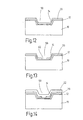
- FIG. 11 shows a layer arrangement which by further processing of the layer arrangement according to FIG 10 has emerged.
- this further processing were the protruding metal surfaces, that is the metal surfaces outside the recess 50, by chemical-mechanical Polishing (CMP) removed. It comes for example metal selective CMP or silicon selective CMP in question.
- CMP chemical-mechanical Polishing
- FIG. 13 shows a state in which the passivation layer 20, which is still contiguous in FIG. 12, is provided with an interruption 62. In this way the surface of the GMR structure 14 is partially exposed.
- FIG. 14 a state is shown in which an electrical Contact to the GMR layer is made.
- a contact metal 22 on the arrangement has been deposited according to FIG. This poses under the mediation of the recess 62 an electrical connection to the GMR structure 14 ago.
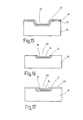
- FIG. 15 shows the result of a method step, which builds on the state of Figure 10.
- the figures 15 to 17 thus show a part of a variant of With reference to the figures 8 to 14 described method.
- a passivation layer 18 deposited so that the GMR layer 14 practically through the passivation layer throughout the process covered and protected.
- FIG. 18 becomes a low temperature PECVD oxide used.
- FIG. 16 shows the final state of a method step, which emanates from the state according to FIG.
- the process step was a planarization by CMP process, for example by an oxide CMP process, carried out.
- FIG. 17 shows the final state of a method step, which builds on the state of FIG 16.
- About the Whole structure according to Figure 16 has been a passivation layer 20 deposited. This serves to passivate the in Figure 16 still open edges of the GMR layer 14. This Step according to FIG. 17 is optional.
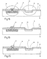
- Figure 18 shows a sectional view through a Layer arrangement.
- a recess 50 is provided, which the pre-structuring for the future GMR structure represents.
- the area 28 are already structured for integrated circuits 24.
- a conductive connection 34 is provided between the first region 26 and the second region 28 .
- the first area 26 has a layer sequence of semiconductor substrate 10, a lower oxide layer 30, the conductive layer 50 and a upper oxide layer 12.
- the upper oxide layer 12 is covered the entire arrangement, that is also the components in area 28.
- the oxide layer acts 12 as a passivation layer.
- FIG 19 a state is shown, which consists of a Processing of the structure according to FIG 18 results.
- the following is the metallic multilayer partially removed by chemical mechanical polishing (CMP). Only in the recess 50 remains the metallic Multiple layer as GMR structure 14.
- the GMR structure 14 is thus directly conductive with the integrated circuit 24 connected.
- the integrated circuit 24 may be, for example an evaluation circuit for the GMR structure be.
Landscapes
- Physics & Mathematics (AREA)
- Chemical & Material Sciences (AREA)
- Engineering & Computer Science (AREA)
- Nanotechnology (AREA)
- Condensed Matter Physics & Semiconductors (AREA)
- General Physics & Mathematics (AREA)
- Crystallography & Structural Chemistry (AREA)
- Internal Circuitry In Semiconductor Integrated Circuit Devices (AREA)
- Hall/Mr Elements (AREA)
- Transmission And Conversion Of Sensor Element Output (AREA)
Abstract
Description
- Figur 1
- einen ersten Zustand während eines Herstellungsverfahrens einer GMR-Struktur des Standes der Technik;
- Figur 2
- einen zweiten Zustand während eines Herstellungsverfahrens einer GMR-Struktur des Standes der Technik;
- Figur 3
- einen dritten Zustand während eines Herstellungsverfahrens einer GMR-Struktur des Standes der Technik;
- Figur 4
- einen vierten Zustand während eines Herstellungsverfahrens einer GMR-Struktur des Standes der Technik;
- Figur 5
- einen fünften Zustand während eines Herstellungsverfahrens einer GMR-Struktur des Standes der Technik;
- Figur 6
- einen sechsten Zustand während eines Herstellungsverfahrens einer GMR-Struktur des Standes der Technik;
- Figur 7
- einen siebten Zustand während eines Herstellungsverfahrens einer GMR-Struktur des Standes der Technik;
- Figur 8
- einen ersten Zustand während eines Herstellungsverfahrens einer GMR-Struktur gemäß der vorliegenden Erfindung;
- Figur 9
- einen zweiten Zustand während eines Herstellungsverfahrens einer GMR-Struktur gemäß der vorliegenden Erfindung;
- Figur'10
- einen dritten Zustand während eines Herstellungsverfahrens einer GMR-Struktur gemäß der vorliegenden Erfindung;
- Figur 11
- einen vierten Zustand während eines Herstellungsverfahrens einer GMR-Struktur gemäß der vorliegenden Erfindung;
- Figur 12
- einen fünften Zustand während eines Herstellungsverfahrens einer GMR-Struktur gemäß der vorliegenden Erfindung;
- Figur 13
- einen sechsten Zustand während eines Herstellungsverfahrens einer GMR-Struktur gemäß der vorliegenden Erfindung;
- Figur 14
- einen siebten Zustand während eines Herstellungsverfahrens einer GMR-Struktur gemäß der vorliegenden Erfindung;
- Figur 15
- einen vierten Zustand während eines Herstellungsverfahrens einer GMR-Struktur gemäß einer weiteren Ausführungsform der vorliegenden Erfindung;
- Figur 16
- einen fünften Zustand während eines Herstellungsverfahrens einer GMR-Struktur gemäß einer weiteren Ausführungsform der vorliegenden Erfindung;
- Figur 17
- einen sechsten Zustand während eines Herstellungsverfahrens einer GMR-Struktur gemäß einer weiteren Ausführungsform der vorliegenden Erfindung;
- Figur 18
- ein Halbleitersubstrat mit Bereichen für eine GMR-Struktur und eine integrierte Schaltung in einem ersten Verarbeitungszustand;
- Figur 19
- ein Halbleitersubstrat mit Bereichen für eine GMR-Struktur und eine integrierte Schaltung in einem zweiten Verarbeitungszustand und
- Figur 20
- ein Halbleitersubstrat mit Bereichen für eine GMR-Struktur und eine integrierte .Schaltung in einem dritten Verarbeitungszustand.
Claims (13)
- Verfahren zum Herstellen einer GMR-Struktur,dadurch gekennzeichnet,bei dem auf einem einen Träger (10) bildenden Halbleitersubstrat eine metallische Vielfachschicht (14) aufgebracht wird undbei dem die metallische Vielfachschicht (14) zum Erzeugen der GMR-Struktur strukturiert wird,dass der Träger (10, 30, 34) vor dem Aufbringen der metallischen Vielfachsrhirht durch eine Vertiefung strukturiert wird,dass auf den strukturierten Träger (10, 30, 34) eine Isolationsschicht (12) aufgebracht wird,dass die metallische Vielfachschicht (14) auf die Isolationsschicht (12) des strukturierten Trägers (10, 30, 34) aufgebracht wirdund dass das Strukturieren der metallischen Vielfachschicht (14) durch chemisch mechanisches Polieren CMP erfolgt.
- Verfahren nach Anspruch 1, dadurch gekennzeichnet, dass die Isolationsschicht (12) durch Abscheiden erzeugt wird.
- Verfahren nach Anspruch 1 oder 2, dadurch gekennzeichnet, dass vor dem Strukturieren der metallischen Vielfachschicht (14) durch chemisch mechanisches Polieren CMP eine Passivierungsschicht (18) abgeschieden wird.
- Verfahren nach einem der vorangehenden Ansprüche, dadurch gekennzeichnet, dass nach dem Strukturieren der mechanischen Vielfachschicht (14) durch chemisch mechanisches Polieren CMP eine Passivierungsschicht (20) auf der metallischen Vielfachschicht (14) abgeschieden wird.
- Verfahren nach einem der vorangehenden Ansprüche, dadurch gekennzeichnet,dass sich nach und/oder vor dem Strukturieren der metallischen Vielfachschicht (14) durch chemisch mechanisches Polieren CMP abgeschiedene Passivierungsschicht (18, 20) strukturiert wird unddass nachfolgend ein Kontaktmetall (22) abgeschieden wird, zur Herstellung einer elektrisch leitenden Verbindung.
- Verfahren nach einem der vorangehenden Ansprüche, dadurch gekennzeichnet, dass das Strukturieren des Halbleitersubstrates (10) im Rahmen der Strukturierung eine integrierten Schaltung (24) auf demselben Halbleitersubstrat (10) erfolgt.
- Verfahren nach einem der vorangehenden Ansprüche, dadurch gekennzeichnet,dass die metallische Vielfachschicht (14) in einem ersten Bereich (26) aufgebracht wird, in welchem die GMR-Struktur erzeugt werden soll unddass die metallische Vielfachschicht (14) in einem zweiten Bereich (28) aufgebracht wird, in welchen Strukturen für eine integrierte Schaltung (24) vorliegen.
- Verfahren nach einem der vorangehenden Ansprüche, dadurch gekennzeichnet,dass vor dem Abscheiden der Isolationsschicht (12) eine weitere Isolationsschicht (30) aufgebracht wird,dass auf die weitere Isolationsschicht (30) eine Schicht (32) aufgebracht wird, welche mindestens eine leitende Verbindung (34) zwischen dem ersten Bereich (26) und dem zweiten Bereich (28) zur Verfügung stellt, unddass nach dem Abscheiden der Isolationsschicht (12) dle Isolationsschicht (12) in dem ersten Bereich (26) strukturiert wird, so dass die nachfolgend aufgebrachte metallische Vielfachschicht (14) einen elektrischen Kontakt zu der mindestens einen elektrischen Verbindung (34) hat.
- Verfahren nach einem der vorangehenden Ansprüche, dadurch gekennzeichnet,dass die Isolationsschicht (12) in einem ersten Bereich (26) aufgebracht wird, in welchem die GMR-Struktur erzeugt werden soll,dass die Isolationsschicht (12) in einem zweiten Bereich (28) aufgebracht wird, in welchem Strukturen für eine integrierte Schaltung (24) vorliegend, unddass die Isolationsschicht (12) in dem zweiten Bereich (28) als Passivierungsschicht wirkt.
- GMR-Struktur mitdadurch gekennzeichnet,einem den Träger (10) bildenden Halbleitersubstrat, auf dem eine Isolationsschicht (12) aufgebracht ist undeiner auf der Isolationsschicht (12) angeordneten strukturierenden metallischen Vielfachschicht,dass die strukturierende metallische Vielfachschicht (14) in einer oder mehreren Vertiefungen (50) des Trägers (10) auf der Isolationsschicht (12) angeordnet ist.
- GMR-Struktur nach Anspruch 10, dadurch gekennzeichnet, dass auf der strukturierten metallischen Vielfachschicht (14) mindestens eine Passivierungsschicht (18,20) angeordnet ist.
- GMR-Struktur nach einem der Ansprüche 10 oder11, dadurch gekennzeichnet,dass auf dem Halbleitersubstrat (10) eine integrierte Schaltung (24) vorgesehen ist,dass zwischen der integrierten Schaltung (24) und der metallischen Vielfachschicht (14) mindestens eine leitende Verbindung (34) besteht, welche unterhalb der metallischen Vielfachschicht (14) angeordnet ist, unddass die Kontaktierung der metallischen Vielfachschicht (14) mit der leitenden Verbindung (34) durch eine Öffnung in einer Isolationsschicht (12) realisiert ist.
- Verwendung einer GMR-Struktur nach einem der Ansprüche 10 bis 12 oder einer nach einem der Ansprüche 1 bis 9 hergestellten GMR-Struktur als Weg- und/oder Winkelsensor.
Applications Claiming Priority (3)
| Application Number | Priority Date | Filing Date | Title |
|---|---|---|---|
| DE10103868A DE10103868A1 (de) | 2001-01-30 | 2001-01-30 | GMR-Struktur und Verfahren zu deren Herstellung |
| DE10103868 | 2001-01-30 | ||
| PCT/DE2002/000243 WO2002061446A1 (de) | 2001-01-30 | 2002-01-25 | Gmr-struktur und verfahren zu deren herstellung |
Publications (2)
| Publication Number | Publication Date |
|---|---|
| EP1358502A1 EP1358502A1 (de) | 2003-11-05 |
| EP1358502B1 true EP1358502B1 (de) | 2005-10-26 |
Family
ID=7672055
Family Applications (1)
| Application Number | Title | Priority Date | Filing Date |
|---|---|---|---|
| EP02701230A Expired - Lifetime EP1358502B1 (de) | 2001-01-30 | 2002-01-25 | Gmr-struktur und verfahren zu deren herstellung |
Country Status (5)
| Country | Link |
|---|---|
| US (1) | US7202544B2 (de) |
| EP (1) | EP1358502B1 (de) |
| JP (1) | JP4518462B2 (de) |
| DE (2) | DE10103868A1 (de) |
| WO (1) | WO2002061446A1 (de) |
Families Citing this family (3)
| Publication number | Priority date | Publication date | Assignee | Title |
|---|---|---|---|---|
| DE102011077907B4 (de) * | 2011-06-21 | 2013-07-11 | Leibniz-Institut Für Festkörper- Und Werkstoffforschung Dresden E.V. | Verfahren zur herstellung von gedruckten magnetischen funktionselementen für widerstandssensoren und gedruckte magnetische funktionselemente |
| JP5886967B2 (ja) * | 2011-09-14 | 2016-03-16 | リージェンツ オブ ザ ユニバーシティ オブ ミネソタ | 外部磁界を必要としない磁気生体センサ |
| WO2013059692A1 (en) | 2011-10-19 | 2013-04-25 | Regents Of The University Of Minnesota | Magnetic biomedical sensors and sensing system for high-throughput biomolecule testing |
Family Cites Families (13)
| Publication number | Priority date | Publication date | Assignee | Title |
|---|---|---|---|---|
| JPS6243811A (ja) * | 1985-08-21 | 1987-02-25 | Hitachi Ltd | 薄膜ヘツド |
| FR2671220B1 (fr) * | 1990-12-27 | 1995-02-17 | Thomson Csf | Procede de fabrication de capteurs magneto-resistifs, et dispositif magnetique realise suivant un tel procede. |
| DE59406156D1 (de) * | 1993-02-11 | 1998-07-16 | Siemens Ag | Verfahren zur Herstellung einer dreidimensionalen Schaltungsanordnung |
| DE4314539C2 (de) | 1993-05-03 | 1998-11-05 | Siemens Ag | Magnetowiderstands-Sensor mit vertikaler Empfindlichkeit und Verwendung des Sensors |
| JPH08221719A (ja) | 1995-02-16 | 1996-08-30 | Tdk Corp | スピンバルブ磁気抵抗ヘッド及びその製造方法 |
| JP3549076B2 (ja) * | 1996-02-13 | 2004-08-04 | 矢崎総業株式会社 | 磁気抵抗素子装置 |
| US5650958A (en) | 1996-03-18 | 1997-07-22 | International Business Machines Corporation | Magnetic tunnel junctions with controlled magnetic response |
| JP3544141B2 (ja) * | 1998-05-13 | 2004-07-21 | 三菱電機株式会社 | 磁気検出素子および磁気検出装置 |
| JP3523509B2 (ja) * | 1998-11-27 | 2004-04-26 | シャープ株式会社 | 半導体装置の製造方法 |
| US6153443A (en) * | 1998-12-21 | 2000-11-28 | Motorola, Inc. | Method of fabricating a magnetic random access memory |
| JP4138254B2 (ja) * | 1999-02-26 | 2008-08-27 | インフィネオン テクノロジーズ アクチエンゲゼルシャフト | 記憶セル構造、およびこれを製造する方法 |
| US6445003B1 (en) * | 1999-05-11 | 2002-09-03 | Lg.Philips Lcd Co., Ltd. | Thin film transistor (TFT) type optical detecting sensor |
| JP2002100010A (ja) * | 2000-09-26 | 2002-04-05 | Toshiba Corp | ヨーク型再生磁気ヘッドおよびその製造方法ならびに磁気ディスク装置 |
-
2001
- 2001-01-30 DE DE10103868A patent/DE10103868A1/de not_active Ceased
-
2002
- 2002-01-25 US US10/470,956 patent/US7202544B2/en not_active Expired - Fee Related
- 2002-01-25 EP EP02701230A patent/EP1358502B1/de not_active Expired - Lifetime
- 2002-01-25 JP JP2002561960A patent/JP4518462B2/ja not_active Expired - Fee Related
- 2002-01-25 WO PCT/DE2002/000243 patent/WO2002061446A1/de not_active Ceased
- 2002-01-25 DE DE50204678T patent/DE50204678D1/de not_active Expired - Lifetime
Also Published As
| Publication number | Publication date |
|---|---|
| EP1358502A1 (de) | 2003-11-05 |
| US7202544B2 (en) | 2007-04-10 |
| WO2002061446A1 (de) | 2002-08-08 |
| US20040115922A1 (en) | 2004-06-17 |
| JP4518462B2 (ja) | 2010-08-04 |
| DE10103868A1 (de) | 2002-08-22 |
| DE50204678D1 (de) | 2005-12-01 |
| JP2004518301A (ja) | 2004-06-17 |
Similar Documents
| Publication | Publication Date | Title |
|---|---|---|
| DE10028640B4 (de) | Wheatstonebrücke, beinhaltend Brückenelemente, bestehend aus einem Spin-Valve-System, sowie ein Verfahren zu deren Herstellung | |
| DE19922136B4 (de) | Magnetfeld-Erfassungselement und Magnetfeld-Erfassungseinrichtung | |
| DE69933440T2 (de) | Digitaler magnetischer signalkoppler | |
| DE69534013T2 (de) | Magnetfeldfühler und Verfahren zu ihrer Herstellung | |
| DE102005047414B4 (de) | Magnetoresistives Sensormodul und Verfahren zum Herstellen desselben | |
| EP0371069A1 (de) | Verfahren zur herstellung von mikrosensoren mit integrierter signalverarbeitung | |
| DE4434912A1 (de) | Verfahren zur Herstellung einer Sensoreinrichtung mit GMR-Sensorelementen | |
| DE102021105660A1 (de) | Magnetischer sensor und sein herstellungsverfahren | |
| DE102011085955A1 (de) | XMR-Sensoren mit ausgeprägter Formanisotropie | |
| DE19829609A1 (de) | Verfahren zur Herstellung eines Mikrosystems sowie ein Mikrosystem | |
| DE3346643A1 (de) | Sensor fuer magnetisierbare materialien | |
| EP1963227B1 (de) | Mikromechanisches bauelement und herstellungsverfahren | |
| DE102005005320A1 (de) | Magnetisches Sensorgerät und dessen Herstellungsverfahren | |
| DE19850460B4 (de) | Magnetfelddetektor | |
| EP1157388A1 (de) | Speicherzellenanordnung und verfahren zu deren herstellung | |
| WO2015189023A1 (de) | Magnetfeldsensoranordnung, entsprechendes herstellungsverfahren und betriebsverfahren | |
| DE102006023170A1 (de) | Ausbilden von Via-Kontakten in MRAM-Zellen | |
| DE19949714A1 (de) | Magnetisch sensitives Bauteil, insbesondere Sensorelement, mit magnetoresistiven Schichtsystemen in Brückenschaltung | |
| DE102011008704A1 (de) | Dünnfilm-Magnetsensor und Verfahren zu seiner Herstellung | |
| DE19932308A1 (de) | Sensor, insbesondere Thermosensor, und Verfahren zur Herstellung einer weitgehend freitragenden Membran | |
| DE10019408C2 (de) | Feldeffekttransistor, insbesondere zur Verwendung als Sensorelement oder Beschleunigungssensor, und Verfahren zu dessen Herstellung | |
| DE2504500A1 (de) | Verfahren zur herstellung eines musters aus einer oder mehreren schichten auf einer unterlage durch oertliche entfernung dieser schicht oder schichten durch sputteraetzen und gegenstaende, insbesondere halbleiteranordnungen, die unter verwendung dieses verfahrens hergestellt sind | |
| DE19819456B4 (de) | Verfahren zur Herstellung eines mikromechanischen Bauelements | |
| EP1358502A1 (de) | Gmr-struktur und verfahren zu deren herstellung | |
| DE10107666C1 (de) | Herstellungsverfahren für eine integrierte Schaltung, insbesondere eine Antifuse |
Legal Events
| Date | Code | Title | Description |
|---|---|---|---|
| PUAI | Public reference made under article 153(3) epc to a published international application that has entered the european phase |
Free format text: ORIGINAL CODE: 0009012 |
|
| 17P | Request for examination filed |
Effective date: 20030901 |
|
| AK | Designated contracting states |
Kind code of ref document: A1 Designated state(s): AT BE CH CY DE DK ES FI FR GB GR IE IT LI LU MC NL PT SE TR |
|
| AX | Request for extension of the european patent |
Extension state: AL LT LV MK RO SI |
|
| GRAP | Despatch of communication of intention to grant a patent |
Free format text: ORIGINAL CODE: EPIDOSNIGR1 |
|
| GRAS | Grant fee paid |
Free format text: ORIGINAL CODE: EPIDOSNIGR3 |
|
| GRAA | (expected) grant |
Free format text: ORIGINAL CODE: 0009210 |
|
| AK | Designated contracting states |
Kind code of ref document: B1 Designated state(s): DE GB IT SE |
|
| REG | Reference to a national code |
Ref country code: GB Ref legal event code: FG4D Free format text: NOT ENGLISH |
|
| REF | Corresponds to: |
Ref document number: 50204678 Country of ref document: DE Date of ref document: 20051201 Kind code of ref document: P |
|
| PG25 | Lapsed in a contracting state [announced via postgrant information from national office to epo] |
Ref country code: SE Free format text: LAPSE BECAUSE OF FAILURE TO SUBMIT A TRANSLATION OF THE DESCRIPTION OR TO PAY THE FEE WITHIN THE PRESCRIBED TIME-LIMIT Effective date: 20060126 |
|
| GBT | Gb: translation of ep patent filed (gb section 77(6)(a)/1977) |
Effective date: 20060215 |
|
| PLBE | No opposition filed within time limit |
Free format text: ORIGINAL CODE: 0009261 |
|
| STAA | Information on the status of an ep patent application or granted ep patent |
Free format text: STATUS: NO OPPOSITION FILED WITHIN TIME LIMIT |
|
| 26N | No opposition filed |
Effective date: 20060727 |
|
| PGFP | Annual fee paid to national office [announced via postgrant information from national office to epo] |
Ref country code: IT Payment date: 20120126 Year of fee payment: 11 |
|
| PGFP | Annual fee paid to national office [announced via postgrant information from national office to epo] |
Ref country code: DE Payment date: 20130326 Year of fee payment: 12 Ref country code: GB Payment date: 20130122 Year of fee payment: 12 |
|
| REG | Reference to a national code |
Ref country code: DE Ref legal event code: R119 Ref document number: 50204678 Country of ref document: DE |
|
| GBPC | Gb: european patent ceased through non-payment of renewal fee |
Effective date: 20140125 |
|
| REG | Reference to a national code |
Ref country code: DE Ref legal event code: R119 Ref document number: 50204678 Country of ref document: DE Effective date: 20140801 |
|
| PG25 | Lapsed in a contracting state [announced via postgrant information from national office to epo] |
Ref country code: DE Free format text: LAPSE BECAUSE OF NON-PAYMENT OF DUE FEES Effective date: 20140801 |
|
| PG25 | Lapsed in a contracting state [announced via postgrant information from national office to epo] |
Ref country code: GB Free format text: LAPSE BECAUSE OF NON-PAYMENT OF DUE FEES Effective date: 20140125 |
|
| PG25 | Lapsed in a contracting state [announced via postgrant information from national office to epo] |
Ref country code: IT Free format text: LAPSE BECAUSE OF NON-PAYMENT OF DUE FEES Effective date: 20140125 |