EP1355464A2 - Suppression du courant continu dans un récepteur optique - Google Patents
Suppression du courant continu dans un récepteur optique Download PDFInfo
- Publication number
- EP1355464A2 EP1355464A2 EP03008097A EP03008097A EP1355464A2 EP 1355464 A2 EP1355464 A2 EP 1355464A2 EP 03008097 A EP03008097 A EP 03008097A EP 03008097 A EP03008097 A EP 03008097A EP 1355464 A2 EP1355464 A2 EP 1355464A2
- Authority
- EP
- European Patent Office
- Prior art keywords
- signal
- trans
- level
- impedance amplifier
- differential
- Prior art date
- Legal status (The legal status is an assumption and is not a legal conclusion. Google has not performed a legal analysis and makes no representation as to the accuracy of the status listed.)
- Granted
Links
Images


Classifications
-
- H—ELECTRICITY
- H04—ELECTRIC COMMUNICATION TECHNIQUE
- H04B—TRANSMISSION
- H04B10/00—Transmission systems employing electromagnetic waves other than radio-waves, e.g. infrared, visible or ultraviolet light, or employing corpuscular radiation, e.g. quantum communication
- H04B10/60—Receivers
-
- H—ELECTRICITY
- H04—ELECTRIC COMMUNICATION TECHNIQUE
- H04L—TRANSMISSION OF DIGITAL INFORMATION, e.g. TELEGRAPHIC COMMUNICATION
- H04L25/00—Baseband systems
- H04L25/02—Details ; arrangements for supplying electrical power along data transmission lines
- H04L25/06—Dc level restoring means; Bias distortion correction ; Decision circuits providing symbol by symbol detection
- H04L25/061—Dc level restoring means; Bias distortion correction ; Decision circuits providing symbol by symbol detection providing hard decisions only; arrangements for tracking or suppressing unwanted low frequency components, e.g. removal of dc offset
- H04L25/062—Setting decision thresholds using feedforward techniques only
-
- H—ELECTRICITY
- H04—ELECTRIC COMMUNICATION TECHNIQUE
- H04B—TRANSMISSION
- H04B10/00—Transmission systems employing electromagnetic waves other than radio-waves, e.g. infrared, visible or ultraviolet light, or employing corpuscular radiation, e.g. quantum communication
- H04B10/60—Receivers
- H04B10/66—Non-coherent receivers, e.g. using direct detection
- H04B10/69—Electrical arrangements in the receiver
Definitions
- the present invention relates to a burst-mode optical receiver, and more particularly, to a burst-mode optical receiver for enhancing an available bit rate in an passive network, and to a corresponding operation method.
- optical subscriber networks such as FTTH (Fiber to the Home) will be required to install optical fiber lines directly to the homes of subscribers for the transmissions/receptions of information at a higher speed.
- the subscriber networks have been traditionally constructed with copper based lines. As such, it would be very costly to replace them with the fiber based lines.
- a passive optical network PON has been taken into consideration to provide a more cost-effective optical subscriber network.
- FIG 1 illustrates a general PON system.
- the PON is generally made up of an optical line termination (OLT) located in a central office, a 1xN passive optical splitter, a plurality of optical network units (ONUs) corresponding to each subscriber.
- OLT optical line termination
- ONUs optical network units
- each node is designed to transmit data or packets to other nodes using a predetermined time slot.
- a plurality of subscribers can make use of a single optical line through which desired data are transmitted or received according to a time division multiplexing scheme.
- burst-mode data are generated in which received data or packets have different sizes and phases from each other due to the optical loss or attenuation generated via different transmission routes.
- Each subscriber transmits data at the respective assigned time, but the packets received at the receiving ends are not uniform in size due to the path differences between the OLT and each subscriber.
- an optical receiver As each received packet has a different size and phase due to the optical loss or by different transmission routes between the nodes, an optical receiver must be employed. To this end, a burst-mode optical receiver is used to enable the received packets to have the same sizes and phases.
- the conventional burst-mode optical receivers prevent the loss of burst data caused by a charging/discharging time by the capacitor of the receiver by removing the DC block capacitor.
- a threshold value is extracted from each received packet by the receiver which functions as a reference signal for the purpose of data discrimination, and the data is amplified using the extracted discrimination reference signal.
- FIG 2 is a circuit diagram of a conventional burst-mode optical receiver.
- the burst-mode optical receiver of FIG 2 includes an optical detector 1 for converting input optical signals into current signals, and a trans-impedance amplifier (TIA) 2 for converting current signals passing through the optical detector 1 into voltage signals.
- TIA 2 is dc-coupled.
- Signals received by the optical detector 1 are amplified at the TIA 2 and then divided into two parts, of which one is dc-coupled to and inputted into a differential amplifier of a limiter amplifier 4 and the other is inputted into a circuit for an automatic threshold controller (ATC) 3.
- the ATC 3 extracts discrimination thresholds of the respective packets received from the TIA 2.
- the limiter amplifier 4 amplifies signals with a different optical intensity into signals having a constant amplitude using the extracted discrimination thresholds.
- the thresholds that vary according to the sizes of packets outputted from the ATC 3 are inputted into an input terminal as a reference voltage V ref of the differential amplifier of the limiter amplifier 4 to be amplified and recovered.
- FIG 3 is a circuit diagram of another conventional burst-mode optical receiver having a structure with a differential input/output feedback amplifier.
- the optical receiver of FIG 3 includes an optical detector 8, a differential preamplifier 10, a peak detector 20, and a limiting amplifier 30.
- the peak detector 20 detects the peak value of an output signal to generate a reference voltage so as to set the discrimination thresholds of received packets.
- the limiting amplifier 30 amplifies recovered signals using the generated reference voltage.
- the differential preamplifier 10 is operative to receive current signals, which are detected at the optical detector 8, as inputs and then outputs corresponding voltages. A ratio of the input current to the output voltage, i.e., a trans-impedance, is determined by a feedback resistor Z T .
- the peak detector 20 is made up of an amplifier 22, a drive transistor 24, a buffer transistor 26, a charging capacitor C PD , and a bias circuit 28.
- a reference voltage V ref which is outputted from the peak detector 20, is converted into a discrimination threshold current by the feedback resistor Z T .
- the "+" input terminal of the amplifier 12 receives the current I IN outputted from the optical detector 8, and the "-" output terminal receives the reference voltage V ref or a reference signal.
- the reference signal inputted to the "-" output terminal is a discrimination threshold current converted from the reference voltage V ref , which is detected from the peak detector 20. Accordingly, the differential preamplifier 10 generates output voltages V o + and V o - depending on the difference between the two input currents.
- the output voltage V o + outputted from the "+" terminal of the amplifier 12 in the differential preamplifier 10 is inputted to a "+” terminal of a amplifier 22 of the peak detector 20, whereas the reference voltage V ref applied to the "-" terminal of the amplifier 12 of the differential preamplifier 10 is fed back to a "-" terminal of the amplifier 22 of the peak detector 20. Therefore, when these two voltages are not same at the amplifier 22 of the peak detector 20, the drive transistor 24 is turned on and causes the charging capacitor C PD to be charged with voltage until the "+" and "-" terminals of the amplifier 22 have the same voltage.
- the drive transistor 24 is turned off, and thus the charging capacitor C PD is discharged. With this discharge, the buffer transistor 26 is turned on, and thus current flows through the bias circuit 28. Thereafter, the reference voltage V ref applied to a node between the buffer transistor 26 and the bias circuit 28 and then converted into a discrimination threshold current by the feedback resistor Z T, and finally fed back to the "-" terminal of the amplifier 12 of the differential preamplifier 10.
- the current flowing to the "-" terminal of the amplifier 22 of the peak detector 20 corresponds to a middle value of the optical detection signal I IN current.
- the reference signal V ref functions as the discrimination threshold of the differential preamplifier 10.
- the actual reference signal V ref is typically accompanied with an offset of the differential preamplifier 10, resulting from device asymmetry as well as a structural offset caused by the turn-on voltages of transistors resulting from a circuit structure of the peak detector 20.
- the actual reference signal tend to deviate from a mean or middle level of the output data signal.
- a pulse width distortion is generated due to the change in the reference signal which in turn degenerates the sensitivity of the optical detector 8.
- the conventional feedback burst-mode optical receiver employs a current source I ADJ , which is connected to the "+" input terminal and the resistor Z T of the differential preamplifier 10.
- the current source I ADJ serves to compensate the offset generated by the differential preamplifier 10, but does not compensate the structural offset generated by the turn-on voltages of the transistors within the peak detector 20.
- the reference signal generated from the peak detector 20 is not matched with the mean level of the output data signal, thus still generates a pulse width distortion and degrades the sensitivity the optical detector.
- One aspect of the present invention provides an additional circuit for precisely adjusting the offsets caused by a peak detector, so that a reset signal is generated automatically and a reference voltage signal is set exactly to a middle level.
- Still another aspect is that the present invention may be realized in a simple, reliable, and inexpensive implementation.
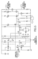
- FIG. 5 is a circuit diagram of an AGC according to the embodiment of the present invention.
- the AGC 140 is constructed to generate the AGC control signal which is generated by the variation of input signal and is not generated at the low input signal level, when the transistors Q1 and Q2 are turned off by the bottom level of the output signal from the TIA 110.
- the signal received in the bottom level detector 120 begins to be distorted at its bottom level during the amplification operation by the TIA 110.
- the AGC 140 begins to operate automatically whenever the output signal of the TIA 110 begins to be distorted. This way, the AGC 140 is able to compensates the gain characteristic based on the level of an input signal.
- the AGC 140 includes a signal level determining section 142 having a resistor R3 and transistors Q3, Q4, and Q5.
- the signal level determining section 142 is configured to analyze the bottom level of a signal input to the base of the transistor Q1 to determine whether the signal is present.
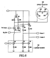
- FIG. 6 is a circuit diagram of a differential buffer 150 according to the embodiment of the present invention.
- the output from the TIA 110 is applied to a base of the transistor Q1, and the signal reference voltage Sig-Ref indicative of the value between the bottom level voltage and the top level voltage is applied to a base of the transistor Q2.
- These transistors Q1 and Q2 are formed into a differential amplifier.
- a power source is supplied to the respective transistors Q1 and Q2 through a transistor Q5.
- Collectors of the transistors Q1 and Q2 are connected to bases of the transistors Q3 and Q4, respectively.
- the differential buffer 150 includes a current source 152(not shown).
- Emitters of the transistors Q6, Q7 and Q8 are connected to the ground through resistors 220, 222 and 224, respectively.
- the current source 152 functions to adjust the amount of current of an emitter terminal constantly.
- Transistors Q3 and Q4 allows two outputs of the differential amplifier, which is made up of transistors Q1 and Q2, to be outputted through the respective emitters.
- an offset adjustor 252 is provided which includes resistors 230, 232, 234 and 236.
- a power level detector 160 is provided for detecting the power level of an input signal.
- the power level detector 160 determines whether or not an effective signal or the output data (+, -) level is present from an output signal of the TIA 110 and provides the determined resultant to a pulse generator 170, and wherein the effective signal means a final output of TIA. That is, the power level detector 160 determines whether or not the effective signal is present and generates a signal related to a loss of signal (LOS). Then, the pulse generator 170 generates a pulse depending on the determined resultant provided from the power level detector 160.
- LOS loss of signal
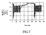
- a symbol of Vin is a signal representing the current outputted from the optical detector 108 and inputted to the TIA 110.
- the TIA 110 amplifies the inputted current to output the amplified current.
- the symbol of Vbot represents the bottom level that the bottom level detector 120 detects from signals supplied from the TIA 110, and a symbol of Sig_REF represents the reference voltage generated by resistors R1 and R2 to which the bottom and top level voltages are applied. As shown in FIG. 7, the reference voltage corresponds almost exactly to the mean level between the top level and the bottom level.
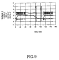
- the signal reference voltage Sig_Ref is generated within the burst-mode optical receiver, and the differential output signals are generated through the internal differential buffer.
- ATC automatic threshold controller
Applications Claiming Priority (2)
| Application Number | Priority Date | Filing Date | Title |
|---|---|---|---|
| KR1020020020489A KR100630089B1 (ko) | 2002-04-15 | 2002-04-15 | 차동 출력 구조의 버스트모드 광 수신기 |
| KR2002020489 | 2002-04-15 |
Publications (3)
| Publication Number | Publication Date |
|---|---|
| EP1355464A2 true EP1355464A2 (fr) | 2003-10-22 |
| EP1355464A3 EP1355464A3 (fr) | 2006-11-02 |
| EP1355464B1 EP1355464B1 (fr) | 2009-03-18 |
Family
ID=28673098
Family Applications (1)
| Application Number | Title | Priority Date | Filing Date |
|---|---|---|---|
| EP03008097A Expired - Fee Related EP1355464B1 (fr) | 2002-04-15 | 2003-04-15 | Suppression du courant continu dans un récepteur optique |
Country Status (5)
| Country | Link |
|---|---|
| US (1) | US7218865B2 (fr) |
| EP (1) | EP1355464B1 (fr) |
| JP (1) | JP2003318680A (fr) |
| KR (1) | KR100630089B1 (fr) |
| DE (1) | DE60326671D1 (fr) |
Cited By (2)
| Publication number | Priority date | Publication date | Assignee | Title |
|---|---|---|---|---|
| US7394996B2 (en) | 2004-06-16 | 2008-07-01 | Industrial Technology Research Institute | Burst mode optical receiver and system and method therefor |
| EP2180567A1 (fr) | 2008-10-22 | 2010-04-28 | CTS Cable Tray Systems SAS | Bras de console antisismique |
Families Citing this family (20)
| Publication number | Priority date | Publication date | Assignee | Title |
|---|---|---|---|---|
| KR100630083B1 (ko) * | 2002-04-26 | 2006-09-27 | 삼성전자주식회사 | 버스트모드 광 수신기의 자동이득조절 장치 |
| KR100554163B1 (ko) * | 2003-03-29 | 2006-02-22 | 한국전자통신연구원 | 수신된 광신호의 소광비 특성을 고려한 버스트 모드 광수신장치 |
| EP2161833B1 (fr) * | 2003-07-30 | 2011-11-30 | Mitsubishi Denki Kabushiki Kaisha | Circuit de commutation de gain pour préamplificateur |
| WO2005055416A1 (fr) * | 2003-12-03 | 2005-06-16 | Matsushita Electric Industrial Co., Ltd. | Preamplificateur photorecepteur |
| KR100601048B1 (ko) * | 2004-04-22 | 2006-07-14 | 한국전자통신연구원 | 버스트 모드 패킷의 수신기 및 그 패킷의 수신 방법 |
| JP4556481B2 (ja) * | 2004-05-14 | 2010-10-06 | 住友電気工業株式会社 | 光送受信器 |
| CN100446443C (zh) * | 2005-08-26 | 2008-12-24 | 电子科技大学 | 一种光突发模式接收机 |
| US7733886B2 (en) * | 2005-12-08 | 2010-06-08 | Electronics And Telecommunications Research Institute | Burst data reception method and apparatus in EPON |
| US7783205B1 (en) * | 2006-01-26 | 2010-08-24 | Universal Electronics Inc. | Learning infrared amplifier for remote control devices |
| KR100751920B1 (ko) * | 2006-04-11 | 2007-08-24 | 고려대학교 산학협력단 | 광수신 장치 |
| US7587145B2 (en) * | 2006-06-29 | 2009-09-08 | Intel Corporation | Optical receiver with electric ternary coding |
| ITTO20060515A1 (it) * | 2006-07-14 | 2008-01-15 | St Microelectronics Srl | "dispositivo per rivelare il valore di picco di un segnale" |
| US7889815B2 (en) * | 2007-02-13 | 2011-02-15 | Optical Communication Products, Inc. | Burst mode receiver for passive optical network |
| EP2120372A1 (fr) * | 2007-02-16 | 2009-11-18 | Fujitsu Limited | Récepteur de lumière |
| JP4940988B2 (ja) * | 2007-02-19 | 2012-05-30 | 富士通オプティカルコンポーネンツ株式会社 | 光受信装置 |
| US20120166117A1 (en) | 2010-10-29 | 2012-06-28 | Xia Llc | Method and apparatus for evaluating superconducting tunnel junction detector noise versus bias voltage |
| JP5894869B2 (ja) * | 2012-06-21 | 2016-03-30 | 株式会社日立製作所 | トランスインピーダンスアンプ |
| JP6443194B2 (ja) * | 2015-04-13 | 2018-12-26 | 富士通株式会社 | 信号識別回路、これを用いた光受信器、及び信号識別方法 |
| CN105007125A (zh) * | 2015-06-01 | 2015-10-28 | 上海市共进通信技术有限公司 | 具有强光保护功能的光网络终端装置及方法 |
| WO2023218623A1 (fr) * | 2022-05-13 | 2023-11-16 | 三菱電機株式会社 | Récepteur optique, dispositif de station maître, et système de communication optique |
Citations (2)
| Publication number | Priority date | Publication date | Assignee | Title |
|---|---|---|---|---|
| US5923219A (en) | 1997-03-19 | 1999-07-13 | Fujitsu Limited | Automatic threshold control circuit and signal amplifying circuit for amplifying signals by compensating for low-frequency response of photodetector |
| EP1006653A2 (fr) | 1998-12-02 | 2000-06-07 | Fujitsu Limited | Circuit amplificateur de signal |
Family Cites Families (11)
| Publication number | Priority date | Publication date | Assignee | Title |
|---|---|---|---|---|
| US5025456A (en) * | 1989-02-02 | 1991-06-18 | At&T Bell Laboratories | Burst mode digital data receiver |
| US5475342A (en) * | 1993-04-19 | 1995-12-12 | Nippon Telegraph And Telephone Corporation | Amplifier for stably maintaining a constant output |
| JPH06334609A (ja) * | 1993-05-26 | 1994-12-02 | Nec Corp | バーストモードディジタル受信器 |
| JPH08102716A (ja) * | 1994-09-30 | 1996-04-16 | Hitachi Ltd | バースト光受信回路 |
| US5953690A (en) * | 1996-07-01 | 1999-09-14 | Pacific Fiberoptics, Inc. | Intelligent fiberoptic receivers and method of operating and manufacturing the same |
| JP3259707B2 (ja) * | 1999-02-26 | 2002-02-25 | 日本電気株式会社 | Agc付きバーストモード光受信回路 |
| JP3674753B2 (ja) * | 1999-03-09 | 2005-07-20 | 富士通株式会社 | バースト信号検出回路 |
| JP3576874B2 (ja) * | 1999-07-15 | 2004-10-13 | シャープ株式会社 | バースト伝送対応光受信器 |
| JP4429565B2 (ja) * | 1999-12-27 | 2010-03-10 | 富士通株式会社 | 信号増幅回路及びこれを用いた光信号受信器 |
| KR100381410B1 (ko) * | 2000-08-23 | 2003-04-23 | 학교법인 한국정보통신학원 | 다단 궤환형 버스트모드 광수신기 |
| KR100605777B1 (ko) * | 2002-04-25 | 2006-07-31 | 삼성전자주식회사 | 버스트모드 광 수신기의 판별 임계값 제어장치 |
-
2002
- 2002-04-15 KR KR1020020020489A patent/KR100630089B1/ko not_active IP Right Cessation
-
2003
- 2003-04-15 DE DE60326671T patent/DE60326671D1/de not_active Expired - Lifetime
- 2003-04-15 US US10/413,979 patent/US7218865B2/en not_active Expired - Fee Related
- 2003-04-15 JP JP2003110899A patent/JP2003318680A/ja active Pending
- 2003-04-15 EP EP03008097A patent/EP1355464B1/fr not_active Expired - Fee Related
Patent Citations (2)
| Publication number | Priority date | Publication date | Assignee | Title |
|---|---|---|---|---|
| US5923219A (en) | 1997-03-19 | 1999-07-13 | Fujitsu Limited | Automatic threshold control circuit and signal amplifying circuit for amplifying signals by compensating for low-frequency response of photodetector |
| EP1006653A2 (fr) | 1998-12-02 | 2000-06-07 | Fujitsu Limited | Circuit amplificateur de signal |
Cited By (3)
| Publication number | Priority date | Publication date | Assignee | Title |
|---|---|---|---|---|
| US7394996B2 (en) | 2004-06-16 | 2008-07-01 | Industrial Technology Research Institute | Burst mode optical receiver and system and method therefor |
| US7657192B2 (en) | 2004-06-16 | 2010-02-02 | Industrial Technology Research Institute | Burst mode optical receiver and system and method therefor |
| EP2180567A1 (fr) | 2008-10-22 | 2010-04-28 | CTS Cable Tray Systems SAS | Bras de console antisismique |
Also Published As
| Publication number | Publication date |
|---|---|
| US20030194244A1 (en) | 2003-10-16 |
| KR100630089B1 (ko) | 2006-09-27 |
| US7218865B2 (en) | 2007-05-15 |
| DE60326671D1 (de) | 2009-04-30 |
| JP2003318680A (ja) | 2003-11-07 |
| EP1355464A3 (fr) | 2006-11-02 |
| KR20030082011A (ko) | 2003-10-22 |
| EP1355464B1 (fr) | 2009-03-18 |
Similar Documents
| Publication | Publication Date | Title |
|---|---|---|
| EP1355464B1 (fr) | Suppression du courant continu dans un récepteur optique | |
| US6909082B2 (en) | Automatic threshold control device for burst mode optical receiver | |
| US8165478B2 (en) | Optical receiver | |
| KR100630083B1 (ko) | 버스트모드 광 수신기의 자동이득조절 장치 | |
| US20130071106A1 (en) | Optical receiver | |
| JP2008211702A (ja) | 前置増幅器およびそれを用いた光受信装置 | |
| US7330670B2 (en) | Bottom level detection device for burst mode optical receiver | |
| KR101544077B1 (ko) | 친국측 장치 | |
| US7266312B2 (en) | Burst mode optical receiver | |
| US7109466B2 (en) | Peak and bottom detectors in burst mode optical receiver | |
| KR100703428B1 (ko) | 버스트모드 광 수신기 및 그의 신호 크기 검출 장치 | |
| KR20040084620A (ko) | 수신된 광신호의 소광비 특성을 고려한 버스트 모드 광수신장치 | |
| KR100381410B1 (ko) | 다단 궤환형 버스트모드 광수신기 | |
| JPH06334609A (ja) | バーストモードディジタル受信器 | |
| JPH11298259A (ja) | 光受信装置及び光受信回路 |
Legal Events
| Date | Code | Title | Description |
|---|---|---|---|
| PUAI | Public reference made under article 153(3) epc to a published international application that has entered the european phase |
Free format text: ORIGINAL CODE: 0009012 |
|
| 17P | Request for examination filed |
Effective date: 20030415 |
|
| AK | Designated contracting states |
Kind code of ref document: A2 Designated state(s): AT BE BG CH CY CZ DE DK EE ES FI FR GB GR HU IE IT LI LU MC NL PT RO SE SI SK TR |
|
| AX | Request for extension of the european patent |
Extension state: AL LT LV MK |
|
| PUAL | Search report despatched |
Free format text: ORIGINAL CODE: 0009013 |
|
| AK | Designated contracting states |
Kind code of ref document: A3 Designated state(s): AT BE BG CH CY CZ DE DK EE ES FI FR GB GR HU IE IT LI LU MC NL PT RO SE SI SK TR |
|
| AX | Request for extension of the european patent |
Extension state: AL LT LV MK |
|
| 17Q | First examination report despatched |
Effective date: 20070426 |
|
| AKX | Designation fees paid |
Designated state(s): DE FR GB |
|
| GRAP | Despatch of communication of intention to grant a patent |
Free format text: ORIGINAL CODE: EPIDOSNIGR1 |
|
| GRAS | Grant fee paid |
Free format text: ORIGINAL CODE: EPIDOSNIGR3 |
|
| GRAA | (expected) grant |
Free format text: ORIGINAL CODE: 0009210 |
|
| AK | Designated contracting states |
Kind code of ref document: B1 Designated state(s): DE FR GB |
|
| REG | Reference to a national code |
Ref country code: GB Ref legal event code: FG4D |
|
| REF | Corresponds to: |
Ref document number: 60326671 Country of ref document: DE Date of ref document: 20090430 Kind code of ref document: P |
|
| PLBE | No opposition filed within time limit |
Free format text: ORIGINAL CODE: 0009261 |
|
| REG | Reference to a national code |
Ref country code: FR Ref legal event code: ST Effective date: 20091231 |
|
| STAA | Information on the status of an ep patent application or granted ep patent |
Free format text: STATUS: NO OPPOSITION FILED WITHIN TIME LIMIT |
|
| 26N | No opposition filed |
Effective date: 20091221 |
|
| PG25 | Lapsed in a contracting state [announced via postgrant information from national office to epo] |
Ref country code: FR Free format text: LAPSE BECAUSE OF NON-PAYMENT OF DUE FEES Effective date: 20091222 |
|
| PGFP | Annual fee paid to national office [announced via postgrant information from national office to epo] |
Ref country code: GB Payment date: 20160311 Year of fee payment: 14 |
|
| PGFP | Annual fee paid to national office [announced via postgrant information from national office to epo] |
Ref country code: DE Payment date: 20160421 Year of fee payment: 14 |
|
| REG | Reference to a national code |
Ref country code: DE Ref legal event code: R119 Ref document number: 60326671 Country of ref document: DE |
|
| GBPC | Gb: european patent ceased through non-payment of renewal fee |
Effective date: 20170415 |
|
| PG25 | Lapsed in a contracting state [announced via postgrant information from national office to epo] |
Ref country code: DE Free format text: LAPSE BECAUSE OF NON-PAYMENT OF DUE FEES Effective date: 20171103 |
|
| PG25 | Lapsed in a contracting state [announced via postgrant information from national office to epo] |
Ref country code: GB Free format text: LAPSE BECAUSE OF NON-PAYMENT OF DUE FEES Effective date: 20170415 |