EP1346255B1 - Mikrolinsenarray mit variabler brennweite zur korrektur der bildfeldwölbung - Google Patents
Mikrolinsenarray mit variabler brennweite zur korrektur der bildfeldwölbung Download PDFInfo
- Publication number
- EP1346255B1 EP1346255B1 EP01988388A EP01988388A EP1346255B1 EP 1346255 B1 EP1346255 B1 EP 1346255B1 EP 01988388 A EP01988388 A EP 01988388A EP 01988388 A EP01988388 A EP 01988388A EP 1346255 B1 EP1346255 B1 EP 1346255B1
- Authority
- EP
- European Patent Office
- Prior art keywords
- opto
- substrate
- array
- micro lens
- electronic devices
- Prior art date
- Legal status (The legal status is an assumption and is not a legal conclusion. Google has not performed a legal analysis and makes no representation as to the accuracy of the status listed.)
- Expired - Lifetime
Links
- 230000005693 optoelectronics Effects 0.000 claims abstract description 90
- 239000000758 substrate Substances 0.000 claims description 40
- 230000003287 optical effect Effects 0.000 abstract description 35
- 238000000926 separation method Methods 0.000 abstract description 11
- 238000000034 method Methods 0.000 description 20
- 238000003491 array Methods 0.000 description 10
- 230000004075 alteration Effects 0.000 description 5
- 238000010586 diagram Methods 0.000 description 3
- 238000005516 engineering process Methods 0.000 description 3
- 238000004519 manufacturing process Methods 0.000 description 3
- JBRZTFJDHDCESZ-UHFFFAOYSA-N AsGa Chemical compound [As]#[Ga] JBRZTFJDHDCESZ-UHFFFAOYSA-N 0.000 description 2
- 229910001218 Gallium arsenide Inorganic materials 0.000 description 2
- 230000008901 benefit Effects 0.000 description 2
- 239000007788 liquid Substances 0.000 description 2
- 239000013307 optical fiber Substances 0.000 description 2
- 229920000642 polymer Polymers 0.000 description 2
- 239000004065 semiconductor Substances 0.000 description 2
- 229910052710 silicon Inorganic materials 0.000 description 2
- 239000010703 silicon Substances 0.000 description 2
- 239000000654 additive Substances 0.000 description 1
- 230000000996 additive effect Effects 0.000 description 1
- 238000004891 communication Methods 0.000 description 1
- 230000007423 decrease Effects 0.000 description 1
- 230000008021 deposition Effects 0.000 description 1
- 238000003384 imaging method Methods 0.000 description 1
Images


Classifications
-
- H—ELECTRICITY
- H01—ELECTRIC ELEMENTS
- H01L—SEMICONDUCTOR DEVICES NOT COVERED BY CLASS H10
- H01L27/00—Devices consisting of a plurality of semiconductor or other solid-state components formed in or on a common substrate
- H01L27/14—Devices consisting of a plurality of semiconductor or other solid-state components formed in or on a common substrate including semiconductor components sensitive to infrared radiation, light, electromagnetic radiation of shorter wavelength or corpuscular radiation and specially adapted either for the conversion of the energy of such radiation into electrical energy or for the control of electrical energy by such radiation
- H01L27/144—Devices controlled by radiation
- H01L27/146—Imager structures
- H01L27/14601—Structural or functional details thereof
- H01L27/14625—Optical elements or arrangements associated with the device
- H01L27/14627—Microlenses
-
- B—PERFORMING OPERATIONS; TRANSPORTING
- B29—WORKING OF PLASTICS; WORKING OF SUBSTANCES IN A PLASTIC STATE IN GENERAL
- B29D—PRODUCING PARTICULAR ARTICLES FROM PLASTICS OR FROM SUBSTANCES IN A PLASTIC STATE
- B29D11/00—Producing optical elements, e.g. lenses or prisms
- B29D11/00009—Production of simple or compound lenses
- B29D11/00278—Lenticular sheets
- B29D11/00298—Producing lens arrays
-
- G—PHYSICS
- G02—OPTICS
- G02B—OPTICAL ELEMENTS, SYSTEMS OR APPARATUS
- G02B6/00—Light guides; Structural details of arrangements comprising light guides and other optical elements, e.g. couplings
- G02B6/10—Light guides; Structural details of arrangements comprising light guides and other optical elements, e.g. couplings of the optical waveguide type
- G02B6/12—Light guides; Structural details of arrangements comprising light guides and other optical elements, e.g. couplings of the optical waveguide type of the integrated circuit kind
- G02B6/12002—Three-dimensional structures
-
- G—PHYSICS
- G02—OPTICS
- G02B—OPTICAL ELEMENTS, SYSTEMS OR APPARATUS
- G02B6/00—Light guides; Structural details of arrangements comprising light guides and other optical elements, e.g. couplings
- G02B6/10—Light guides; Structural details of arrangements comprising light guides and other optical elements, e.g. couplings of the optical waveguide type
- G02B6/12—Light guides; Structural details of arrangements comprising light guides and other optical elements, e.g. couplings of the optical waveguide type of the integrated circuit kind
- G02B6/13—Integrated optical circuits characterised by the manufacturing method
- G02B6/138—Integrated optical circuits characterised by the manufacturing method by using polymerisation
-
- G—PHYSICS
- G02—OPTICS
- G02B—OPTICAL ELEMENTS, SYSTEMS OR APPARATUS
- G02B6/00—Light guides; Structural details of arrangements comprising light guides and other optical elements, e.g. couplings
- G02B6/24—Coupling light guides
- G02B6/42—Coupling light guides with opto-electronic elements
- G02B6/4201—Packages, e.g. shape, construction, internal or external details
- G02B6/4249—Packages, e.g. shape, construction, internal or external details comprising arrays of active devices and fibres
-
- G—PHYSICS
- G02—OPTICS
- G02B—OPTICAL ELEMENTS, SYSTEMS OR APPARATUS
- G02B7/00—Mountings, adjusting means, or light-tight connections, for optical elements
- G02B7/02—Mountings, adjusting means, or light-tight connections, for optical elements for lenses
- G02B7/04—Mountings, adjusting means, or light-tight connections, for optical elements for lenses with mechanism for focusing or varying magnification
-
- H—ELECTRICITY
- H01—ELECTRIC ELEMENTS
- H01L—SEMICONDUCTOR DEVICES NOT COVERED BY CLASS H10
- H01L31/00—Semiconductor devices sensitive to infrared radiation, light, electromagnetic radiation of shorter wavelength or corpuscular radiation and specially adapted either for the conversion of the energy of such radiation into electrical energy or for the control of electrical energy by such radiation; Processes or apparatus specially adapted for the manufacture or treatment thereof or of parts thereof; Details thereof
- H01L31/02—Details
- H01L31/0232—Optical elements or arrangements associated with the device
- H01L31/02325—Optical elements or arrangements associated with the device the optical elements not being integrated nor being directly associated with the device
-
- H—ELECTRICITY
- H01—ELECTRIC ELEMENTS
- H01L—SEMICONDUCTOR DEVICES NOT COVERED BY CLASS H10
- H01L31/00—Semiconductor devices sensitive to infrared radiation, light, electromagnetic radiation of shorter wavelength or corpuscular radiation and specially adapted either for the conversion of the energy of such radiation into electrical energy or for the control of electrical energy by such radiation; Processes or apparatus specially adapted for the manufacture or treatment thereof or of parts thereof; Details thereof
- H01L31/02—Details
- H01L31/0232—Optical elements or arrangements associated with the device
- H01L31/02327—Optical elements or arrangements associated with the device the optical elements being integrated or being directly associated to the device, e.g. back reflectors
-
- G—PHYSICS
- G02—OPTICS
- G02B—OPTICAL ELEMENTS, SYSTEMS OR APPARATUS
- G02B6/00—Light guides; Structural details of arrangements comprising light guides and other optical elements, e.g. couplings
- G02B6/24—Coupling light guides
- G02B6/42—Coupling light guides with opto-electronic elements
- G02B6/4201—Packages, e.g. shape, construction, internal or external details
- G02B6/4204—Packages, e.g. shape, construction, internal or external details the coupling comprising intermediate optical elements, e.g. lenses, holograms
- G02B6/4206—Optical features
-
- G—PHYSICS
- G02—OPTICS
- G02B—OPTICAL ELEMENTS, SYSTEMS OR APPARATUS
- G02B6/00—Light guides; Structural details of arrangements comprising light guides and other optical elements, e.g. couplings
- G02B6/24—Coupling light guides
- G02B6/42—Coupling light guides with opto-electronic elements
- G02B6/4201—Packages, e.g. shape, construction, internal or external details
- G02B6/4204—Packages, e.g. shape, construction, internal or external details the coupling comprising intermediate optical elements, e.g. lenses, holograms
- G02B6/4214—Packages, e.g. shape, construction, internal or external details the coupling comprising intermediate optical elements, e.g. lenses, holograms the intermediate optical element having redirecting reflective means, e.g. mirrors, prisms for deflecting the radiation from horizontal to down- or upward direction toward a device
Definitions
- This invention relates to the field of opto-electronic devices apd more particularly to opto-electronic devices with optical micro lenses.
- Opto-electronic devices include both emitters and detectors.
- An opto-electronic emitter is a device that converts an electrical signal into an optical signal. Examples of opto-electronic emitters include light emitting diodes (LEDs) and vertical cavity surface emitting lasers (VCSELs).
- An opto-electronic detector is a device that converts an optical signal into an electrical signal. Examples of opto-electronic detectors include Charge Coupled Devices (CCDs) and resonant cavity photodetectors (RCPDs).
- CCDs Charge Coupled Devices
- RCPDs resonant cavity photodetectors
- an external fore lens is often employed to focus or collimate the beams of light to or from the array.
- aberrations are often associated with the fore lens.
- One common aberration is a curvature of field aberration, which causes the light to be focused on a curved surface, such as a sphere, rather than on the surface of a plane.
- Other more complex aberrations are also common.
- Prior art methods for compensating for field curvature include implementing a refractive field-flatting element. Unfortunately, these refractive field-flattening elements are both costly and bulky. Therefore, a need exists for an economical and compact method for reducing the curvature of field associated with the fore lens in an optical system.
- the present invention overcomes many of the disadvantages of the prior art by providing a method and apparatus for compensating for an aberration, such as a curvature of field, of a fore lens in a system that includes one or more optoelectronic devices.
- US-A-6021003, US-A-5439621 and JP-A-62065013 all disclose the concept of using a micro lens array having varying focal length to flatten the focal field. Further relevant documents are US5526182 and EP-A-1026672.
- the present invention provides a focal field corrector as defined in claim 1, comprising:
- each micro lens is situated on one of said plurality of surfaces, and each micro lens is situated to compensate for a non-planar focal field of a fore lens to appear substantially planar at the first surface of the first substrate.
- each micro lens is separated from the fore optic (and thus a corresponding optoelectronic device) by a distance that depends on the location of the micro lens relative to the optical axis of the fore optic.
- the separation distance between each micro lens and the fore optic is related to, and may track, the non-planar fore optic image surface.
- Each micro lens may also have a focal length that corresponds to the separation distance between the micro lens and the corresponding opto-electronic device so that the light captured by the micro lens can be effectively relayed or focused to the aperture of the corresponding opto-electronic device.
- the array of opto-electronic devices are opto-electronic detectors, such as resonant cavity photo detectors (RCPDs) or charge coupled devices (CCDs).
- the array of opto-electronic devices are opto-electronic emitters, such as vertical cavity surface emitting lasers (VCSELs) or light emitting diodes (LEDs).
- the array of opto-electronic devices includes a combination of detectors and emitter, such as VCSELs and RCPDs.
- Another illustrative embodiment of the present invention includes an optical system that has multiple opto-electronic arrays configured in a two-dimensional array on a substrate.
- Each opto-electronic array includes a plurality of opto-electronic devices and a corresponding fore optic provided above the opto-electronic array.
- Each opto-electronic array may be either centered or offset from the optical axis of the corresponding fore optic.
- each opto-electronic array may include emitters, detectors, or a combination of emitters and detectors.
- Figure 1 is a cross-sectional representation of an optical system than includes a fore optic 4, such as a lens, provided above an array of opto-electronic devices 6.
- a fore optic 4 such as a lens
- Fore optic 4 transforms light 2 such that it is incident on the array of opto-electronic devices 6.
- the array of opto-electronic devices 6 includes a center axis 7, which may be centered or offset from optical axis 5 of fore optic 4.
- the array of opto-electronic devices 6 includes opto-electronic devices 8, 10, 12, 14, and 16 integrated on a common substrate 18.
- Substrate 18 is preferably a semiconductor substrate such as silicon or GaAs.
- Opto-electronic devices 8, 10, 12, 14, 16, and 18 may be any type of opto-electronic device know to those skilled in the art, including, for example, CCDs, RCPDs, LEDs, and VCSELs.
- Fore optic 4 has optical axis 5 and a non-planar focal field, such as curvature of field 20 substantially centered along optical axis 5.
- a non-planar focal field such as curvature of field 20 substantially centered along optical axis 5.
- the curvature of field 20 has a spherical shape as shown.
- the optical signal at the opto-electronic device 12 in the center of the array of opto-electronic devices 6 may be greater than the optical signal at the opto-electronic devices 8 and 16 near the outside of the array of opto-electronic devices.
- optical signal at each of the opto-electronic devices may depend on the location of the opto-electronic device relative to the particular image surface.
- Figure 2 is a top view of an array of opto-electronic devices such as those discussed in reference to Figure 1.
- Line 1-1 represents the line from which the cross-section of Figure 1 is taken.
- Figure 2 represents a square two-dimensional array.
- the present invention is not limited to a square array.
- the detectors can be fabricated in any suitable one or two-dimensional configuration.
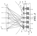
- Figure 3 is a cross-sectional representation of an optical system that includes an array of opto-electronic devices in accordance with the present invention.
- the embodiment shown in Figure 3 is similar to that shown in Figure 1, except a number of co-planar micro lenses 24, 26, 28, 30, and 32 have been added above opto-electronic devices 8, 10, 12, 14, and 16, respectively.
- the coplanar micro lenses 24, 26, 28, 30, and 32 are preferably initially fabricated on an optically transparent substrate 36, which is then bonded to the substrate 18 that includes the array of opto-electronic devices 8, 10, 12, 14, and 16.
- Fore optic 4 collimates or focuses the light rays 2 along an image surface 20 defined by the field of curvature of the fore optic 4.
- Each micro lens preferably has a focal length that compensates for the field of curvature of the fore optic 4.
- the focal lengths of micro lenses 24, 26, 28, 30, and 32 may increase monotonically away from central optical axis 5 of fore optic 4.
- the light rays 2 that are transmitted through fore optic 4 may be substantially focused by the micro lenses 24, 26, 28, 30, and 32 to the planar surface 34 of the array of opto-electronic devices 6.
- the optical signal at each of the opto-electronic devices may depend on the location of the opto-electronic device relative to the image surface of the fore optic.
- the focal length of the micro lenses may not necessarily increase monotonically, but may vary according to the particular image surface of the fore optic, preferably so that the aperture of the corresponding opto-electronic device is focused or relayed onto the fore optic image surface.
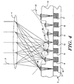
- Figure 4 is a cross-sectional view of another optical system in accordance with the present invention, which includes an array of non-planar micro lenses, each having a corresponding opto-electronic device.
- the embodiment shown in Figure 4 is similar to that shown in Figure 3, except the micro lenses 40, 42, 44, 46, 48, 50 and 52 are non-planar, and have a varying separation distance from the fore optic 4 (and thus the opto-electronic devices 3, 8, 10, 12, 14, 16, and 17 respectively).
- the separation distance between the micro lenses 40, 42, 44, 46, 48, 50 and 52 and the fore optic 4 By varying the separation distance between the micro lenses 40, 42, 44, 46, 48, 50 and 52 and the fore optic 4, more of the light that is focused on the non-planar focal field 20 of the fore optic 4 can be captured by the micro lenses.
- each micro lens 40, 42, 44, 46, 48, 50 and 52 has a focal length that corresponds to the separation distance between the micro lens and the corresponding opto-electronic device so that the light captured by the micro lens can be relayed or focused at the aperture of the corresponding opto-electronic device.
- the embodiment shown in Figure 4 has the benefit of moving the micro lenses closer to the fore optic image surface, thereby capturing more of the light coming to focus at the image surface. This may permit each of the micro lenses to have substantially the same width or diameter, as shown.
- the embodiment shown in Figure 3 may not necessarily permit a constant micro lens width, which may be a detriment when the width or diameter of some of the micro lenses approach or exceed the pitch of the opto-electronic devices.
- the non-planar micro lenses 40, 42, 44, 46, 48, 50 and 52 of Figure 4 are preferably initially fabricated on an optically transparent substrate 54, which is then bonded to the substrate 18 that includes the array of opto-electronic devices 3, 8, 10, 12, 14, 16 and 17.
- a number of methods for providing a varying separation distance between the micro lens 40, 42, 44, 46, 48, 50 and 52 and the array of opto-electronic devices 3, 8, 10, 12, 14, 16 and 17 are contemplated. Some of the methods use an additive process, such as a deposition or growth process. Other methods use a subtractive process.
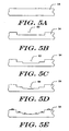
- FIGS. 5A-5E One illustrative method for providing a varying separation distance between the micro lens 40, 42, 44, 46, 48, 50 and 52 and the array of opto-electronic devices 3, 8, 10, 12, 14, 16 and 17 is shown in Figures 5A-5E.
- An optically transparent substrate 54 is provided in Figure 5A.
- a first groove or cavity 60 is etched into the top surface of substrate 54, preferably using known methods.
- the first groove or cavity 60 may provide a surface for forming one or more micro lenses, as further described below.
- a second groove or cavity 62 may be etched into the bottom surface of the first groove or cavity 60, as shown.
- the second groove or cavity 62 may provide another lower surface for forming one or more micro lenses.
- a third groove or cavity 64 may be etched into the bottom surface of the second groove or cavity 62, as shown.
- the third groove or cavity 64 may provide yet another lower surface for forming one or more micro lenses:
- a fourth groove or cavity 66 may be etched into the bottom surface of the third groove or cavity 64.
- the fourth groove or cavity 66 may provide another lower surface for forming one or more micro lenses.
- Figure 5E shows non-planar micro lenses 40, 42, 44, 46, 48, 50 and 52 formed on the various step surfaces etched into the optically transparent substrate 54.
- the optically transparent substrate 54 shown in Figure 5E can be used for providing compensation for a fore optic that has a "spherical-like" image surface.
- the various steps or surfaces formed in the optically transparent substrate 54 may be tailored to provide a suitable separation distance for each micro lens that helps compensate for the non-planar and more complex image surfaces.
- the array of opto-electronic devices illustrated in Figures 3-4 are not limited to either opto-electronic emitters or opto-electronic detectors exclusively.
- the optical system can easily be modified to include both emitters and detectors in a single array.
- One method used to fabricate emitters and detectors is illustrated in U.S. Patent Application Serial No. 08/736,803, entitled "Monolithic Vertical Cavity Surface Emitting Laser and Resonant Cavity Photodetector Transceiver," which is incorporated herein by reference.
- emitters and detectors fabricated separately may be physically and electronically connected to a single substrate. Methods for connecting independent devices on a single substrate may include wire bonding, bump technology, or the like.
- FIG. 6 is a perspective view of yet another optical system of the present invention.
- multiple opto-electronic arrays 70 are provided in a two-dimensional configuration on substrate 74.
- Each opto-electronic array 70 includes a plurality of opto-electronic devices and a corresponding fore optic 76.
- Each opto-electronic device 72 in opto-electronic array 70 has a corresponding micro lens (not shown).
- Each fore optic 76 may have a non-planar focal field, such as a curvature of field.
- each micro lens can be fabricated to have a corresponding focal length and/or separation distance that compensates for the non-planar focal field of fore optic 76.
- FIG 6 there are four opto-electronic arrays each including four opto-electronic devices.
- Figure 6 is merely illustrative however, and the present invention is not limited to the number or type of arrays and devices shown therein.
- multiple opto-electronic arrays 70 may be fabricated on a single substrate, such as substrate 74.
- Substrate 74 is preferably a semiconductor substrate such as a silicon or gallium arsenide wafer.
- opto-electronic arrays may be fabricated on an individual substrate 78 that is in turn physically bonded to or electronically connected to substrate 74.
- An electronic connection to substrate 74 may be provided through the use of bonding technology well know to those skilled in the art, such as wire bonding, bump technology, or the like.
- Each opto-electronic array 70 may contain opto-electronic emitters, such as VCSELs or LEDs, opto-electronic detectors, such as RCPDs or CCDs, or a combination of detectors and emitters, such as VCSELs and RCPDs. Therefore, fore optic 76 may provide light 80 both to and/or from opto-electronic array 70. Light 80 provided to fore optic 76 from opto-electronic array 70 may be in turn provided to another optical device (not shown) such as a mirror, lens, optical fiber, or optical detector. Alternatively, light 80 may be provided through fore optic 76 to opto-electronic device 72, for example, from an optical device such as a mirror, lens, optical fiber, or optical emitter.
- opto-electronic emitters such as VCSELs or LEDs
- opto-electronic detectors such as RCPDs or CCDs
- a combination of detectors and emitters such as VC
- FIG. 7 is a schematic representation of one method for fabricating the micro lenses used in accordance with the present invention.
- a print head 82 provides a liquid optical polymer 86 via a nozzle 84.
- the liquid optical polymer 86 forms a droplet 88, which is provided to an opto-electronic device 92 on a substrate 94 to form a micro lens 90. While this illustrative method shows the micro lens 90 provided directly on the opto-electronic device 92, it is contemplated that the micro lens may be formed on another, preferably optical transparent substrate, which is then mounted or otherwise attached to the substrate 94 so the micro lenses are in registration with the opto-electronic devices, such as device 92.
- Figures 8(a)-(c) are schematic representations of one method for providing micro lenses with different focal lengths across an array.
- one droplet 88 is provided to an opto-electronic device 92 to form a micro lens 90.
- the micro lens 90 has a focal length f 1 .
- two droplets 88 are successively provided to an opto-electronic device to form a micro lens 96.
- the micro lens 96 has a focal length of f 2 .
- three droplets 88 are successively provided to an opto-electronic device 98 to form a micro lens 98.
- the micro lens 98 has a focal length of f 3 , where f 3 ⁇ f 2 ⁇ f 1 . As the number of droplets increases, the focal length of the corresponding micro lens decreases. Therefore, the focal length of the micro lens 98 is less than the focal length of the micro lens 96, which in turn is less than the focal length of the micro lens 90.
- a more detailed description of one method for forming the micro lenses can be found in U.S. Patent No. 5,707, 684 to Hayes et al., entitled "Method for Producing Micro-Optical Components.”
Claims (8)
- Brennfeldkorrektor, der folgendes umfaßt:ein erstes Substrat (54) mit einer ersten Oberfläche auf einer Seite, die im wesentlichen planar ist, und einer zweiten Oberfläche auf einer gegenüberliegenden Seite, die mehrere abgestufte Oberflächen aufweist, wobei einige der Oberflächen der mehreren Oberflächen sich nicht in einer Ebene relativ zueinander befinden; undmehrere Mikrolinsen (40, 42, 44, 46, 48, 50, 52), wobei sich jede Mikrolinse auf einer der mehreren Oberflächen befindet und jede Mikrolinse so angeordnet ist, daß sie ein nichtplanares Brennfeld einer Vorderlinse (4) kompensiert, um auf der ersten Oberfläche des ersten Substrats (54) im wesentlichen planar zu erscheinen.
- Korrektor nach Anspruch 1, wobei das erste Substrat (54) und die mehreren Mikrolinsen (40, 42, 44, 46, 48, 50, 52) im wesentlichen optisch transparent sind.
- Korrektor nach Anspruch 2, weiterhin umfassend:ein zweites Substrat (18) mit einer im wesentlichen planaren ersten Oberfläche undmehrere optoelektronische Bauelemente (3, 8, 10, 12, 14, 16, 17), die sich in der ersten Oberfläche des zweiten Substrats (18) befinden; undwobei sich die erste Oberfläche des ersten Substrats (54) neben der ersten Oberfläche des zweiten Substrats (18) befindet.
- Korrektor nach Anspruch 3, wobei die mehreren optoelektronischen Bauelemente (3, 8, 10, 12, 14, 16, 17) Emitter und/oder Detektoren sind.
- Korrektor nach Anspruch 4, wobei
die mehreren Oberflächen der zweiten Oberfläche des ersten Substrats (54) mehrere abgestufte und/oder vertiefte Oberflächen sind und
sich mindestens einige der abgestuften und/oder vertieften Oberflächen nicht in der gleichen Ebene befinden. - Korrektor nach Anspruch 5, wobei jedes optoelektronische Bauelement der mehreren optoelektronischen Bauelemente (3, 8, 10, 12, 14, 16, 17) mit jeder Mikrolinse der mehreren Mikrolinsen (40, 42, 44, 46, 48, 50, 52) auf einer Eins-zu-Eins-Basis assoziiert ist.
- Korrektor nach Anspruch 6, wobei jede Mikrolinse so angeordnet ist, daß sie einen entsprechenden Abschnitt des nichtplanaren Brennfeldes der Vorderlinse (4) zweidimensional kompensiert, um auf der ersten Oberfläche des ersten Substrats (54) im wesentlichen planar zu erscheinen.
- Korrektor nach Anspruch 7, wobei die erste Oberfläche des zweiten Substrats (18) an der ersten Oberfläche des ersten Substrats (54) angebracht ist.
Applications Claiming Priority (3)
| Application Number | Priority Date | Filing Date | Title |
|---|---|---|---|
| US749296 | 1996-11-14 | ||
| US09/749,296 US6556349B2 (en) | 2000-12-27 | 2000-12-27 | Variable focal length micro lens array field curvature corrector |
| PCT/US2001/050094 WO2002052335A2 (en) | 2000-12-27 | 2001-12-20 | Variable focal length micro lens array field curvature corrector |
Publications (2)
| Publication Number | Publication Date |
|---|---|
| EP1346255A2 EP1346255A2 (de) | 2003-09-24 |
| EP1346255B1 true EP1346255B1 (de) | 2006-09-13 |
Family
ID=25013142
Family Applications (1)
| Application Number | Title | Priority Date | Filing Date |
|---|---|---|---|
| EP01988388A Expired - Lifetime EP1346255B1 (de) | 2000-12-27 | 2001-12-20 | Mikrolinsenarray mit variabler brennweite zur korrektur der bildfeldwölbung |
Country Status (8)
| Country | Link |
|---|---|
| US (1) | US6556349B2 (de) |
| EP (1) | EP1346255B1 (de) |
| JP (1) | JP2004526300A (de) |
| AT (1) | ATE339708T1 (de) |
| AU (1) | AU2002241700A1 (de) |
| DE (1) | DE60123122T2 (de) |
| TW (1) | TWI254156B (de) |
| WO (1) | WO2002052335A2 (de) |
Families Citing this family (78)
| Publication number | Priority date | Publication date | Assignee | Title |
|---|---|---|---|---|
| US6909554B2 (en) * | 2000-12-27 | 2005-06-21 | Finisar Corporation | Wafer integration of micro-optics |
| WO2003015226A2 (en) * | 2001-08-08 | 2003-02-20 | Santur Corporation | Method and system for selecting an output of a vcsel array |
| DE50210653D1 (de) * | 2001-08-24 | 2007-09-20 | Schott Ag | Verfahren zur herstellung von elektronischen bauelementen |
| JP2003143459A (ja) * | 2001-11-02 | 2003-05-16 | Canon Inc | 複眼撮像系およびこれを備えた装置 |
| US6822995B2 (en) | 2002-02-21 | 2004-11-23 | Finisar Corporation | GaAs/AI(Ga)As distributed bragg reflector on InP |
| JP4291615B2 (ja) * | 2002-05-28 | 2009-07-08 | 株式会社巴川製紙所 | 光学素子ウエハ及びその製造方法、光学素子の製造方法 |
| JP2004101848A (ja) * | 2002-09-09 | 2004-04-02 | Nippon Sheet Glass Co Ltd | マイクロレンズアレイ、マイクロレンズアレイを用いた光モジュール、及び光モジュールの位置決め方法 |
| US6822241B2 (en) * | 2002-10-03 | 2004-11-23 | Hewlett-Packard Development Company, L.P. | Emitter device with focusing columns |
| US20040151828A1 (en) * | 2003-02-04 | 2004-08-05 | Anis Zribi | Method for fabrication and alignment of micro and nanoscale optics using surface tension gradients |
| JP4347599B2 (ja) * | 2003-04-10 | 2009-10-21 | オリンパス株式会社 | 個人認証装置 |
| KR100541028B1 (ko) * | 2003-07-21 | 2006-01-11 | 주식회사 옵토메카 | 이미지 센서 및 그 제조 방법 |
| US7164702B1 (en) | 2003-08-29 | 2007-01-16 | The United States Of America As Represented By The Secretary Of The Army | Optical transmitters and interconnects using surface-emitting lasers and micro-optical elements |
| US7002750B2 (en) * | 2003-11-06 | 2006-02-21 | Ann-Lun Lee | Image capturing device |
| US7280278B2 (en) * | 2004-06-02 | 2007-10-09 | Micron Technology, Inc. | Apparatus and method for manufacturing positive or negative microlenses |
| KR100658930B1 (ko) * | 2004-12-30 | 2006-12-15 | 매그나칩 반도체 유한회사 | 칼라별 초점 거리 조절이 가능한 이미지센서 및 그 제조방법 |
| US7375312B2 (en) * | 2005-01-26 | 2008-05-20 | Avago Technologies Ecbu Ip Pte Ltd | Planar fly's eye detector |
| JP4699917B2 (ja) * | 2006-02-28 | 2011-06-15 | パナソニック株式会社 | 固体撮像素子 |
| JP2007266380A (ja) * | 2006-03-29 | 2007-10-11 | Matsushita Electric Ind Co Ltd | 半導体撮像装置およびその製造方法 |
| DE102006047941B4 (de) * | 2006-10-10 | 2008-10-23 | Fraunhofer-Gesellschaft zur Förderung der angewandten Forschung e.V. | Vorrichtung zur Homogenisierung von Strahlung mit nicht regelmäßigen Mikrolinsenarrays |
| JP5312774B2 (ja) * | 2006-12-15 | 2013-10-09 | 日立オートモティブシステムズ株式会社 | 薄型認証センサ |
| US8319846B2 (en) * | 2007-01-11 | 2012-11-27 | Raytheon Company | Video camera system using multiple image sensors |
| US7692878B2 (en) | 2008-03-03 | 2010-04-06 | General Electric Company | Optical device and method |
| WO2010048618A1 (en) * | 2008-10-24 | 2010-04-29 | Tenebraex Corporation | Systems and methods for high resolution imaging |
| US8400537B2 (en) * | 2008-11-13 | 2013-03-19 | Omnivision Technologies, Inc. | Image sensors having gratings for color separation |
| US8830377B2 (en) * | 2010-01-04 | 2014-09-09 | Duke University | Monocentric lens-based multi-scale optical systems and methods of use |
| US10725280B2 (en) | 2009-01-05 | 2020-07-28 | Duke University | Multiscale telescopic imaging system |
| US9432591B2 (en) | 2009-01-05 | 2016-08-30 | Duke University | Multiscale optical system having dynamic camera settings |
| US9494771B2 (en) * | 2009-01-05 | 2016-11-15 | Duke University | Quasi-monocentric-lens-based multi-scale optical system |
| US8259212B2 (en) * | 2009-01-05 | 2012-09-04 | Applied Quantum Technologies, Inc. | Multiscale optical system |
| US9395617B2 (en) | 2009-01-05 | 2016-07-19 | Applied Quantum Technologies, Inc. | Panoramic multi-scale imager and method therefor |
| US9635253B2 (en) | 2009-01-05 | 2017-04-25 | Duke University | Multiscale telescopic imaging system |
| EP2553319B1 (de) * | 2010-03-31 | 2017-03-01 | Koninklijke Philips N.V. | Beleuchtunsseinheit |
| US20120027417A1 (en) * | 2010-07-30 | 2012-02-02 | Santori Charles M | Optical power divider |
| KR101708807B1 (ko) * | 2010-09-30 | 2017-02-21 | 삼성전자 주식회사 | 이미지 센서 |
| FR2966936B1 (fr) | 2010-11-02 | 2012-12-07 | Commissariat Energie Atomique | Systeme optique de formation d'image sur une surface spherique concave |
| JP2012114384A (ja) * | 2010-11-29 | 2012-06-14 | Kyocera Corp | 光照射デバイスおよび印刷装置 |
| EP2461198A3 (de) | 2010-12-01 | 2017-03-08 | BlackBerry Limited | Vorrichtung und zugehöriges Verfahren für ein Kameramodul einer elektronischen Vorrichtung |
| DE102011107895B4 (de) | 2011-07-18 | 2020-11-05 | Heraeus Noblelight Gmbh | Optoelektronisches Modul mit Linsensystem |
| DE102011052802B4 (de) * | 2011-08-18 | 2014-03-13 | Sick Ag | 3D-Kamera und Verfahren zur Überwachung eines Raumbereichs |
| US20130120621A1 (en) * | 2011-11-10 | 2013-05-16 | Research In Motion Limited | Apparatus and associated method for forming color camera image |
| CN103139470A (zh) * | 2011-11-30 | 2013-06-05 | 索尼公司 | 数字成像系统 |
| JP5801731B2 (ja) * | 2012-01-24 | 2015-10-28 | 株式会社小糸製作所 | 車輌用前照灯 |
| US10334181B2 (en) | 2012-08-20 | 2019-06-25 | Microsoft Technology Licensing, Llc | Dynamically curved sensor for optical zoom lens |
| US9247121B2 (en) * | 2013-04-25 | 2016-01-26 | Ability Enterprise Co., Ltd. | Image sensor, electric device using the same and focusing method of the electric device |
| US9386203B2 (en) * | 2013-10-28 | 2016-07-05 | Omnivision Technologies, Inc. | Compact spacer in multi-lens array module |
| US10139619B2 (en) | 2015-02-12 | 2018-11-27 | Optiz, Inc. | Back side illumination image sensor with non-planar optical interface |
| KR102297488B1 (ko) | 2015-02-17 | 2021-09-02 | 삼성전자주식회사 | 라이트 필드 카메라 |
| CN104867951B (zh) * | 2015-04-23 | 2018-05-04 | 豪威科技(上海)有限公司 | 一种背照式传感器芯片及其制造方法 |
| KR102391485B1 (ko) | 2016-03-17 | 2022-04-28 | 삼성전자주식회사 | 무선 통신 시스템에서 빔을 송신하기 위한 방법 및 장치 |
| US10212785B2 (en) | 2016-06-13 | 2019-02-19 | Google Llc | Staggered array of individually addressable light-emitting elements for sweeping out an angular range |
| US9909862B2 (en) | 2016-06-13 | 2018-03-06 | Google Llc | Curved array of light-emitting elements for sweeping out an angular range |
| US10924638B2 (en) * | 2016-06-27 | 2021-02-16 | Intel Corporation | Compact, low cost VCSEL projector for high performance stereodepth camera |
| CN106024820B (zh) * | 2016-07-04 | 2019-03-26 | 豪威科技(上海)有限公司 | 一种堆栈式图像传感器芯片及其制造方法 |
| KR102381621B1 (ko) | 2017-05-18 | 2022-04-01 | 삼성전자 주식회사 | 렌즈를 포함하는 유리 구조물 및 렌즈를 포함하는 수신기 |
| WO2019108578A1 (en) * | 2017-11-28 | 2019-06-06 | The Charles Stark Draper Laboratory, Inc. | Coupling lens aberration correction through grating design in a switched focal plane array |
| KR102531003B1 (ko) | 2017-12-19 | 2023-05-10 | 삼성전자 주식회사 | 렌즈를 포함하는 빔포밍 안테나 모듈 |
| DE102017130578A1 (de) * | 2017-12-19 | 2019-06-19 | Osram Opto Semiconductors Gmbh | Lichtquelle |
| US10905242B1 (en) | 2018-04-09 | 2021-02-02 | Regalo International, Llc | Character chair |
| KR20190118794A (ko) | 2018-04-11 | 2019-10-21 | 삼성전자주식회사 | 무선 통신 시스템에서 렌즈를 이용하여 빔을 조절하기 위한 장치 및 방법 |
| KR20190118792A (ko) | 2018-04-11 | 2019-10-21 | 삼성전자주식회사 | 무선 통신 시스템에서 렌즈를 이용하여 빔을 제어하기 위한 장치 및 방법 |
| DE102018124040A1 (de) * | 2018-07-24 | 2020-01-30 | Osram Opto Semiconductors Gmbh | Optoelektronische halbleitervorrichtung mit ersten und zweiten optoelektronischen elementen |
| US11333748B2 (en) | 2018-09-17 | 2022-05-17 | Waymo Llc | Array of light detectors with corresponding array of optical elements |
| US11067884B2 (en) * | 2018-12-26 | 2021-07-20 | Apple Inc. | Through-display optical transmission, reception, or sensing through micro-optic elements |
| US11070740B2 (en) | 2019-01-18 | 2021-07-20 | Panasonic I-Pro Sensing Solutions Co., Ltd. | Camera device and IR light irradiating method |
| JP6706707B1 (ja) * | 2019-05-15 | 2020-06-10 | パナソニックi−PROセンシングソリューションズ株式会社 | 集光レンズおよび監視カメラ |
| US10838556B2 (en) | 2019-04-05 | 2020-11-17 | Apple Inc. | Sensing system for detection of light incident to a light emitting layer of an electronic device display |
| US10761243B1 (en) * | 2019-08-26 | 2020-09-01 | Jute Industrial Co., Ltd. | Optical device |
| US11527582B1 (en) | 2019-09-24 | 2022-12-13 | Apple Inc. | Display stack with integrated photodetectors |
| US11611058B2 (en) | 2019-09-24 | 2023-03-21 | Apple Inc. | Devices and systems for under display image sensor |
| US11953625B2 (en) * | 2020-01-27 | 2024-04-09 | The Charles Stark Draper Laboratory, Inc. | Beamsplitter architecture for monostatic LiDAR |
| US11592873B2 (en) | 2020-02-14 | 2023-02-28 | Apple Inc. | Display stack topologies for under-display optical transceivers |
| US11295664B2 (en) | 2020-03-11 | 2022-04-05 | Apple Inc. | Display-synchronized optical emitters and transceivers |
| US11327237B2 (en) | 2020-06-18 | 2022-05-10 | Apple Inc. | Display-adjacent optical emission or reception using optical fibers |
| US11487859B2 (en) | 2020-07-31 | 2022-11-01 | Apple Inc. | Behind display polarized optical transceiver |
| US20220065999A1 (en) * | 2020-08-26 | 2022-03-03 | Voyant Photonics Inc. | Hybrid two-dimensional steering lidar |
| US20220229210A1 (en) * | 2021-01-17 | 2022-07-21 | Apple Inc. | Microlens array with tailored sag profile |
| US11839133B2 (en) | 2021-03-12 | 2023-12-05 | Apple Inc. | Organic photodetectors for in-cell optical sensing |
| WO2023173195A1 (en) * | 2022-03-16 | 2023-09-21 | 10644137 Canada Inc. | Bijective illumination collection imaging apparatus and method thereof |
Family Cites Families (23)
| Publication number | Priority date | Publication date | Assignee | Title |
|---|---|---|---|---|
| US5148322A (en) | 1989-11-09 | 1992-09-15 | Omron Tateisi Electronics Co. | Micro aspherical lens and fabricating method therefor and optical device |
| US5401968A (en) | 1989-12-29 | 1995-03-28 | Honeywell Inc. | Binary optical microlens detector array |
| GB9008577D0 (en) * | 1990-04-17 | 1990-06-13 | Pilkington Diffractive Lenses | Rigid gas permeable lenses |
| US5073041A (en) | 1990-11-13 | 1991-12-17 | Bell Communications Research, Inc. | Integrated assembly comprising vertical cavity surface-emitting laser array with Fresnel microlenses |
| US5325386A (en) | 1992-04-21 | 1994-06-28 | Bandgap Technology Corporation | Vertical-cavity surface emitting laser assay display system |
| US5245622A (en) | 1992-05-07 | 1993-09-14 | Bandgap Technology Corporation | Vertical-cavity surface-emitting lasers with intra-cavity structures |
| US5526182A (en) * | 1993-02-17 | 1996-06-11 | Vixel Corporation | Multiple beam optical memory system |
| US5439621A (en) | 1993-04-12 | 1995-08-08 | Minnesota Mining And Manufacturing Company | Method of making an array of variable focal length microlenses |
| JP2601148B2 (ja) | 1993-07-23 | 1997-04-16 | 日本電気株式会社 | 固体撮像装置 |
| US5498444A (en) | 1994-02-28 | 1996-03-12 | Microfab Technologies, Inc. | Method for producing micro-optical components |
| US5902997A (en) * | 1994-05-20 | 1999-05-11 | Siemens Aktiengesellschaft | Device for spacing at least one lens from an optoelectronic component |
| US5814803A (en) | 1994-12-23 | 1998-09-29 | Spectra-Physics Scanning Systems, Inc. | Image reader with multi-focus lens |
| US5633527A (en) | 1995-02-06 | 1997-05-27 | Sandia Corporation | Unitary lens semiconductor device |
| JP3698794B2 (ja) | 1995-02-27 | 2005-09-21 | オリンパス株式会社 | 光学スキャナ |
| US5693967A (en) | 1995-08-10 | 1997-12-02 | Lg Semicon Co., Ltd. | Charge coupled device with microlens |
| US5812581A (en) | 1996-07-26 | 1998-09-22 | Honeywell Inc. | Lens for a semiconductive device with a laser and a photodetector in a common container |
| US6137535A (en) | 1996-11-04 | 2000-10-24 | Eastman Kodak Company | Compact digital camera with segmented fields of view |
| US6043481A (en) * | 1997-04-30 | 2000-03-28 | Hewlett-Packard Company | Optoelectronic array device having a light transmissive spacer layer with a ridged pattern and method of making same |
| US5966399A (en) | 1997-10-02 | 1999-10-12 | Motorola, Inc. | Vertical cavity surface emitting laser with integrated diffractive lens and method of fabrication |
| JP3509534B2 (ja) | 1998-03-09 | 2004-03-22 | 富士通株式会社 | 光学装置 |
| US6056448A (en) | 1998-04-16 | 2000-05-02 | Lockheed Martin Corporation | Vertical cavity surface emitting laser array packaging |
| US6301363B1 (en) * | 1998-10-26 | 2001-10-09 | The Standard Register Company | Security document including subtle image and system and method for viewing the same |
| JP3368422B2 (ja) * | 1999-01-29 | 2003-01-20 | 富士通株式会社 | レンズ装置、これを用いた光学ヘッドおよび光ディスク装置 |
-
2000
- 2000-12-27 US US09/749,296 patent/US6556349B2/en not_active Expired - Lifetime
-
2001
- 2001-12-20 EP EP01988388A patent/EP1346255B1/de not_active Expired - Lifetime
- 2001-12-20 AT AT01988388T patent/ATE339708T1/de not_active IP Right Cessation
- 2001-12-20 DE DE60123122T patent/DE60123122T2/de not_active Expired - Lifetime
- 2001-12-20 JP JP2002553178A patent/JP2004526300A/ja active Pending
- 2001-12-20 WO PCT/US2001/050094 patent/WO2002052335A2/en active IP Right Grant
- 2001-12-20 AU AU2002241700A patent/AU2002241700A1/en not_active Abandoned
- 2001-12-26 TW TW090132321A patent/TWI254156B/zh not_active IP Right Cessation
Also Published As
| Publication number | Publication date |
|---|---|
| TWI254156B (en) | 2006-05-01 |
| WO2002052335A3 (en) | 2003-02-13 |
| US20030011888A1 (en) | 2003-01-16 |
| DE60123122D1 (de) | 2006-10-26 |
| JP2004526300A (ja) | 2004-08-26 |
| US6556349B2 (en) | 2003-04-29 |
| AU2002241700A1 (en) | 2002-07-08 |
| EP1346255A2 (de) | 2003-09-24 |
| ATE339708T1 (de) | 2006-10-15 |
| DE60123122T2 (de) | 2007-09-13 |
| WO2002052335A2 (en) | 2002-07-04 |
Similar Documents
| Publication | Publication Date | Title |
|---|---|---|
| EP1346255B1 (de) | Mikrolinsenarray mit variabler brennweite zur korrektur der bildfeldwölbung | |
| US6909554B2 (en) | Wafer integration of micro-optics | |
| US7128477B2 (en) | Optical transmitter and receiver module | |
| US6040934A (en) | Receptacle-type optical transmission/reception apparatus | |
| US7352066B2 (en) | Silicon based optical vias | |
| US8755644B2 (en) | Silicon based optical vias | |
| US6931181B2 (en) | Opto-mechanical assembly | |
| US6219470B1 (en) | Wavelength division multiplexing transmitter and receiver module | |
| KR101041570B1 (ko) | 광통신 모듈 | |
| US20190391345A1 (en) | Coupling device having a stamped structured surface for routing optical data signals | |
| US20060239612A1 (en) | Flip-chip devices formed on photonic integrated circuit chips | |
| KR100703464B1 (ko) | 양방향 광 송수신기 | |
| US8987655B2 (en) | Optical module having at least one light receiving element with a wiring part covers a part of a side surface of a mesa part | |
| US20050069013A1 (en) | Method and apparatus for wavelength division multiplexing | |
| WO2011056187A1 (en) | Expanded beam interface device and method for fabricating same | |
| NL2003498C2 (nl) | Opto-elektronische inrichting voor het bidirectioneel via glasvezels transporteren van informatie en werkwijze voor het vervaardigen van een dergelijke inrichting. | |
| US7503706B2 (en) | MSM photodetector assembly | |
| US20050084217A1 (en) | Optical module capable of transmitting optical signal in bi-directional with single fiber | |
| US7076129B2 (en) | Apparatus and method for a filterless parallel WDM multiplexer | |
| JP3795869B2 (ja) | 光モジュール | |
| US7645077B2 (en) | Bi-directional optical communication module | |
| CN113031258A (zh) | 光学系统及其光处理方法 | |
| US20230054560A1 (en) | Microled parallel optical interconnects | |
| JP3096558B2 (ja) | 光通信用受発信モジュール | |
| US20230253518A1 (en) | Semiconductor device and fabricating method therefor |
Legal Events
| Date | Code | Title | Description |
|---|---|---|---|
| PUAI | Public reference made under article 153(3) epc to a published international application that has entered the european phase |
Free format text: ORIGINAL CODE: 0009012 |
|
| 17P | Request for examination filed |
Effective date: 20030701 |
|
| AK | Designated contracting states |
Kind code of ref document: A2 Designated state(s): AT BE CH CY DE DK ES FI FR GB GR IE IT LI LU MC NL PT SE TR |
|
| AX | Request for extension of the european patent |
Extension state: AL LT LV MK RO SI |
|
| 17Q | First examination report despatched |
Effective date: 20040420 |
|
| GRAP | Despatch of communication of intention to grant a patent |
Free format text: ORIGINAL CODE: EPIDOSNIGR1 |
|
| GRAS | Grant fee paid |
Free format text: ORIGINAL CODE: EPIDOSNIGR3 |
|
| GRAA | (expected) grant |
Free format text: ORIGINAL CODE: 0009210 |
|
| AK | Designated contracting states |
Kind code of ref document: B1 Designated state(s): AT BE CH CY DE DK ES FI FR GB GR IE IT LI LU MC NL PT SE TR |
|
| PG25 | Lapsed in a contracting state [announced via postgrant information from national office to epo] |
Ref country code: IT Free format text: LAPSE BECAUSE OF FAILURE TO SUBMIT A TRANSLATION OF THE DESCRIPTION OR TO PAY THE FEE WITHIN THE PRESCRIBED TIME-LIMIT;WARNING: LAPSES OF ITALIAN PATENTS WITH EFFECTIVE DATE BEFORE 2007 MAY HAVE OCCURRED AT ANY TIME BEFORE 2007. THE CORRECT EFFECTIVE DATE MAY BE DIFFERENT FROM THE ONE RECORDED. Effective date: 20060913 Ref country code: LI Free format text: LAPSE BECAUSE OF FAILURE TO SUBMIT A TRANSLATION OF THE DESCRIPTION OR TO PAY THE FEE WITHIN THE PRESCRIBED TIME-LIMIT Effective date: 20060913 Ref country code: AT Free format text: LAPSE BECAUSE OF FAILURE TO SUBMIT A TRANSLATION OF THE DESCRIPTION OR TO PAY THE FEE WITHIN THE PRESCRIBED TIME-LIMIT Effective date: 20060913 Ref country code: NL Free format text: LAPSE BECAUSE OF FAILURE TO SUBMIT A TRANSLATION OF THE DESCRIPTION OR TO PAY THE FEE WITHIN THE PRESCRIBED TIME-LIMIT Effective date: 20060913 Ref country code: BE Free format text: LAPSE BECAUSE OF FAILURE TO SUBMIT A TRANSLATION OF THE DESCRIPTION OR TO PAY THE FEE WITHIN THE PRESCRIBED TIME-LIMIT Effective date: 20060913 Ref country code: FI Free format text: LAPSE BECAUSE OF FAILURE TO SUBMIT A TRANSLATION OF THE DESCRIPTION OR TO PAY THE FEE WITHIN THE PRESCRIBED TIME-LIMIT Effective date: 20060913 Ref country code: CH Free format text: LAPSE BECAUSE OF FAILURE TO SUBMIT A TRANSLATION OF THE DESCRIPTION OR TO PAY THE FEE WITHIN THE PRESCRIBED TIME-LIMIT Effective date: 20060913 |
|
| REG | Reference to a national code |
Ref country code: GB Ref legal event code: FG4D |
|
| REG | Reference to a national code |
Ref country code: CH Ref legal event code: EP |
|
| REG | Reference to a national code |
Ref country code: IE Ref legal event code: FG4D |
|
| REF | Corresponds to: |
Ref document number: 60123122 Country of ref document: DE Date of ref document: 20061026 Kind code of ref document: P |
|
| PG25 | Lapsed in a contracting state [announced via postgrant information from national office to epo] |
Ref country code: SE Free format text: LAPSE BECAUSE OF FAILURE TO SUBMIT A TRANSLATION OF THE DESCRIPTION OR TO PAY THE FEE WITHIN THE PRESCRIBED TIME-LIMIT Effective date: 20061213 Ref country code: DK Free format text: LAPSE BECAUSE OF FAILURE TO SUBMIT A TRANSLATION OF THE DESCRIPTION OR TO PAY THE FEE WITHIN THE PRESCRIBED TIME-LIMIT Effective date: 20061213 |
|
| PG25 | Lapsed in a contracting state [announced via postgrant information from national office to epo] |
Ref country code: IE Free format text: LAPSE BECAUSE OF NON-PAYMENT OF DUE FEES Effective date: 20061220 |
|
| PG25 | Lapsed in a contracting state [announced via postgrant information from national office to epo] |
Ref country code: ES Free format text: LAPSE BECAUSE OF FAILURE TO SUBMIT A TRANSLATION OF THE DESCRIPTION OR TO PAY THE FEE WITHIN THE PRESCRIBED TIME-LIMIT Effective date: 20061224 |
|
| PG25 | Lapsed in a contracting state [announced via postgrant information from national office to epo] |
Ref country code: MC Free format text: LAPSE BECAUSE OF NON-PAYMENT OF DUE FEES Effective date: 20061231 |
|
| PG25 | Lapsed in a contracting state [announced via postgrant information from national office to epo] |
Ref country code: PT Free format text: LAPSE BECAUSE OF FAILURE TO SUBMIT A TRANSLATION OF THE DESCRIPTION OR TO PAY THE FEE WITHIN THE PRESCRIBED TIME-LIMIT Effective date: 20070226 |
|
| NLV1 | Nl: lapsed or annulled due to failure to fulfill the requirements of art. 29p and 29m of the patents act | ||
| REG | Reference to a national code |
Ref country code: CH Ref legal event code: PL |
|
| ET | Fr: translation filed | ||
| PLBE | No opposition filed within time limit |
Free format text: ORIGINAL CODE: 0009261 |
|
| STAA | Information on the status of an ep patent application or granted ep patent |
Free format text: STATUS: NO OPPOSITION FILED WITHIN TIME LIMIT |
|
| 26N | No opposition filed |
Effective date: 20070614 |
|
| PG25 | Lapsed in a contracting state [announced via postgrant information from national office to epo] |
Ref country code: GR Free format text: LAPSE BECAUSE OF FAILURE TO SUBMIT A TRANSLATION OF THE DESCRIPTION OR TO PAY THE FEE WITHIN THE PRESCRIBED TIME-LIMIT Effective date: 20061214 |
|
| PG25 | Lapsed in a contracting state [announced via postgrant information from national office to epo] |
Ref country code: TR Free format text: LAPSE BECAUSE OF FAILURE TO SUBMIT A TRANSLATION OF THE DESCRIPTION OR TO PAY THE FEE WITHIN THE PRESCRIBED TIME-LIMIT Effective date: 20060913 Ref country code: LU Free format text: LAPSE BECAUSE OF NON-PAYMENT OF DUE FEES Effective date: 20061220 |
|
| PG25 | Lapsed in a contracting state [announced via postgrant information from national office to epo] |
Ref country code: CY Free format text: LAPSE BECAUSE OF FAILURE TO SUBMIT A TRANSLATION OF THE DESCRIPTION OR TO PAY THE FEE WITHIN THE PRESCRIBED TIME-LIMIT Effective date: 20060913 |
|
| PGFP | Annual fee paid to national office [announced via postgrant information from national office to epo] |
Ref country code: GB Payment date: 20101123 Year of fee payment: 10 |
|
| PGFP | Annual fee paid to national office [announced via postgrant information from national office to epo] |
Ref country code: FR Payment date: 20111205 Year of fee payment: 11 |
|
| PGFP | Annual fee paid to national office [announced via postgrant information from national office to epo] |
Ref country code: DE Payment date: 20111230 Year of fee payment: 11 |
|
| GBPC | Gb: european patent ceased through non-payment of renewal fee |
Effective date: 20121220 |
|
| REG | Reference to a national code |
Ref country code: FR Ref legal event code: ST Effective date: 20130830 |
|
| REG | Reference to a national code |
Ref country code: DE Ref legal event code: R119 Ref document number: 60123122 Country of ref document: DE Effective date: 20130702 |
|
| PG25 | Lapsed in a contracting state [announced via postgrant information from national office to epo] |
Ref country code: DE Free format text: LAPSE BECAUSE OF NON-PAYMENT OF DUE FEES Effective date: 20130702 |
|
| PG25 | Lapsed in a contracting state [announced via postgrant information from national office to epo] |
Ref country code: GB Free format text: LAPSE BECAUSE OF NON-PAYMENT OF DUE FEES Effective date: 20121220 Ref country code: FR Free format text: LAPSE BECAUSE OF NON-PAYMENT OF DUE FEES Effective date: 20130102 |