EP1345270A2 - Semiconductor device and manufacturing method for the same - Google Patents
Semiconductor device and manufacturing method for the same Download PDFInfo
- Publication number
- EP1345270A2 EP1345270A2 EP02023883A EP02023883A EP1345270A2 EP 1345270 A2 EP1345270 A2 EP 1345270A2 EP 02023883 A EP02023883 A EP 02023883A EP 02023883 A EP02023883 A EP 02023883A EP 1345270 A2 EP1345270 A2 EP 1345270A2
- Authority
- EP
- European Patent Office
- Prior art keywords
- wiring line
- film
- copper
- semiconductor device
- containing metal
- Prior art date
- Legal status (The legal status is an assumption and is not a legal conclusion. Google has not performed a legal analysis and makes no representation as to the accuracy of the status listed.)
- Withdrawn
Links
Images













Classifications
-
- H—ELECTRICITY
- H10—SEMICONDUCTOR DEVICES; ELECTRIC SOLID-STATE DEVICES NOT OTHERWISE PROVIDED FOR
- H10P—GENERIC PROCESSES OR APPARATUS FOR THE MANUFACTURE OR TREATMENT OF DEVICES COVERED BY CLASS H10
- H10P70/00—Cleaning of wafers, substrates or parts of devices
- H10P70/20—Cleaning during device manufacture
- H10P70/27—Cleaning during device manufacture during, before or after processing of conductive materials, e.g. polysilicon or amorphous silicon layers
-
- H—ELECTRICITY
- H10—SEMICONDUCTOR DEVICES; ELECTRIC SOLID-STATE DEVICES NOT OTHERWISE PROVIDED FOR
- H10D—INORGANIC ELECTRIC SEMICONDUCTOR DEVICES
- H10D64/00—Electrodes of devices having potential barriers
- H10D64/01—Manufacture or treatment
- H10D64/011—Manufacture or treatment of electrodes ohmically coupled to a semiconductor
-
- H—ELECTRICITY
- H10—SEMICONDUCTOR DEVICES; ELECTRIC SOLID-STATE DEVICES NOT OTHERWISE PROVIDED FOR
- H10P—GENERIC PROCESSES OR APPARATUS FOR THE MANUFACTURE OR TREATMENT OF DEVICES COVERED BY CLASS H10
- H10P14/00—Formation of materials, e.g. in the shape of layers or pillars
- H10P14/40—Formation of materials, e.g. in the shape of layers or pillars of conductive or resistive materials
- H10P14/42—Formation of materials, e.g. in the shape of layers or pillars of conductive or resistive materials using a gas or vapour
- H10P14/44—Physical vapour deposition [PVD]
-
- H—ELECTRICITY
- H10—SEMICONDUCTOR DEVICES; ELECTRIC SOLID-STATE DEVICES NOT OTHERWISE PROVIDED FOR
- H10P—GENERIC PROCESSES OR APPARATUS FOR THE MANUFACTURE OR TREATMENT OF DEVICES COVERED BY CLASS H10
- H10P70/00—Cleaning of wafers, substrates or parts of devices
- H10P70/20—Cleaning during device manufacture
- H10P70/27—Cleaning during device manufacture during, before or after processing of conductive materials, e.g. polysilicon or amorphous silicon layers
- H10P70/277—Cleaning during device manufacture during, before or after processing of conductive materials, e.g. polysilicon or amorphous silicon layers the processing being a planarisation of conductive layers
-
- H—ELECTRICITY
- H10—SEMICONDUCTOR DEVICES; ELECTRIC SOLID-STATE DEVICES NOT OTHERWISE PROVIDED FOR
- H10W—GENERIC PACKAGES, INTERCONNECTIONS, CONNECTORS OR OTHER CONSTRUCTIONAL DETAILS OF DEVICES COVERED BY CLASS H10
- H10W20/00—Interconnections in chips, wafers or substrates
- H10W20/01—Manufacture or treatment
- H10W20/031—Manufacture or treatment of conductive parts of the interconnections
-
- H—ELECTRICITY
- H10—SEMICONDUCTOR DEVICES; ELECTRIC SOLID-STATE DEVICES NOT OTHERWISE PROVIDED FOR
- H10W—GENERIC PACKAGES, INTERCONNECTIONS, CONNECTORS OR OTHER CONSTRUCTIONAL DETAILS OF DEVICES COVERED BY CLASS H10
- H10W20/00—Interconnections in chips, wafers or substrates
- H10W20/01—Manufacture or treatment
- H10W20/031—Manufacture or treatment of conductive parts of the interconnections
- H10W20/032—Manufacture or treatment of conductive parts of the interconnections of conductive barrier, adhesion or liner layers
- H10W20/033—Manufacture or treatment of conductive parts of the interconnections of conductive barrier, adhesion or liner layers in openings in dielectrics
- H10W20/037—Manufacture or treatment of conductive parts of the interconnections of conductive barrier, adhesion or liner layers in openings in dielectrics the barrier, adhesion or liner layers being on top of a main fill metal
-
- H—ELECTRICITY
- H10—SEMICONDUCTOR DEVICES; ELECTRIC SOLID-STATE DEVICES NOT OTHERWISE PROVIDED FOR
- H10W—GENERIC PACKAGES, INTERCONNECTIONS, CONNECTORS OR OTHER CONSTRUCTIONAL DETAILS OF DEVICES COVERED BY CLASS H10
- H10W20/00—Interconnections in chips, wafers or substrates
- H10W20/01—Manufacture or treatment
- H10W20/031—Manufacture or treatment of conductive parts of the interconnections
- H10W20/056—Manufacture or treatment of conductive parts of the interconnections by filling conductive material into holes, grooves or trenches
-
- H—ELECTRICITY
- H10—SEMICONDUCTOR DEVICES; ELECTRIC SOLID-STATE DEVICES NOT OTHERWISE PROVIDED FOR
- H10W—GENERIC PACKAGES, INTERCONNECTIONS, CONNECTORS OR OTHER CONSTRUCTIONAL DETAILS OF DEVICES COVERED BY CLASS H10
- H10W20/00—Interconnections in chips, wafers or substrates
- H10W20/01—Manufacture or treatment
- H10W20/031—Manufacture or treatment of conductive parts of the interconnections
- H10W20/064—Manufacture or treatment of conductive parts of the interconnections by modifying the conductivity of conductive parts, e.g. by alloying
- H10W20/066—Manufacture or treatment of conductive parts of the interconnections by modifying the conductivity of conductive parts, e.g. by alloying by forming silicides of refractory metals
-
- H—ELECTRICITY
- H10—SEMICONDUCTOR DEVICES; ELECTRIC SOLID-STATE DEVICES NOT OTHERWISE PROVIDED FOR
- H10W—GENERIC PACKAGES, INTERCONNECTIONS, CONNECTORS OR OTHER CONSTRUCTIONAL DETAILS OF DEVICES COVERED BY CLASS H10
- H10W20/00—Interconnections in chips, wafers or substrates
- H10W20/01—Manufacture or treatment
- H10W20/071—Manufacture or treatment of dielectric parts thereof
- H10W20/081—Manufacture or treatment of dielectric parts thereof by forming openings in the dielectric parts
-
- H—ELECTRICITY
- H10—SEMICONDUCTOR DEVICES; ELECTRIC SOLID-STATE DEVICES NOT OTHERWISE PROVIDED FOR
- H10W—GENERIC PACKAGES, INTERCONNECTIONS, CONNECTORS OR OTHER CONSTRUCTIONAL DETAILS OF DEVICES COVERED BY CLASS H10
- H10W20/00—Interconnections in chips, wafers or substrates
- H10W20/01—Manufacture or treatment
- H10W20/071—Manufacture or treatment of dielectric parts thereof
- H10W20/081—Manufacture or treatment of dielectric parts thereof by forming openings in the dielectric parts
- H10W20/084—Manufacture or treatment of dielectric parts thereof by forming openings in the dielectric parts for dual-damascene structures
-
- H—ELECTRICITY
- H10—SEMICONDUCTOR DEVICES; ELECTRIC SOLID-STATE DEVICES NOT OTHERWISE PROVIDED FOR
- H10W—GENERIC PACKAGES, INTERCONNECTIONS, CONNECTORS OR OTHER CONSTRUCTIONAL DETAILS OF DEVICES COVERED BY CLASS H10
- H10W20/00—Interconnections in chips, wafers or substrates
- H10W20/40—Interconnections external to wafers or substrates, e.g. back-end-of-line [BEOL] metallisations or vias connecting to gate electrodes
- H10W20/41—Interconnections external to wafers or substrates, e.g. back-end-of-line [BEOL] metallisations or vias connecting to gate electrodes characterised by their conductive parts
- H10W20/42—Vias, e.g. via plugs
-
- H—ELECTRICITY
- H10—SEMICONDUCTOR DEVICES; ELECTRIC SOLID-STATE DEVICES NOT OTHERWISE PROVIDED FOR
- H10W—GENERIC PACKAGES, INTERCONNECTIONS, CONNECTORS OR OTHER CONSTRUCTIONAL DETAILS OF DEVICES COVERED BY CLASS H10
- H10W20/00—Interconnections in chips, wafers or substrates
- H10W20/40—Interconnections external to wafers or substrates, e.g. back-end-of-line [BEOL] metallisations or vias connecting to gate electrodes
- H10W20/41—Interconnections external to wafers or substrates, e.g. back-end-of-line [BEOL] metallisations or vias connecting to gate electrodes characterised by their conductive parts
- H10W20/425—Barrier, adhesion or liner layers
-
- H—ELECTRICITY
- H10—SEMICONDUCTOR DEVICES; ELECTRIC SOLID-STATE DEVICES NOT OTHERWISE PROVIDED FOR
- H10W—GENERIC PACKAGES, INTERCONNECTIONS, CONNECTORS OR OTHER CONSTRUCTIONAL DETAILS OF DEVICES COVERED BY CLASS H10
- H10W20/00—Interconnections in chips, wafers or substrates
- H10W20/40—Interconnections external to wafers or substrates, e.g. back-end-of-line [BEOL] metallisations or vias connecting to gate electrodes
- H10W20/45—Interconnections external to wafers or substrates, e.g. back-end-of-line [BEOL] metallisations or vias connecting to gate electrodes characterised by their insulating parts
- H10W20/47—Interconnections external to wafers or substrates, e.g. back-end-of-line [BEOL] metallisations or vias connecting to gate electrodes characterised by their insulating parts comprising two or more dielectric layers having different properties, e.g. different dielectric constants
-
- H—ELECTRICITY
- H10—SEMICONDUCTOR DEVICES; ELECTRIC SOLID-STATE DEVICES NOT OTHERWISE PROVIDED FOR
- H10P—GENERIC PROCESSES OR APPARATUS FOR THE MANUFACTURE OR TREATMENT OF DEVICES COVERED BY CLASS H10
- H10P50/00—Etching of wafers, substrates or parts of devices
- H10P50/20—Dry etching; Plasma etching; Reactive-ion etching
- H10P50/26—Dry etching; Plasma etching; Reactive-ion etching of conductive or resistive materials
- H10P50/264—Dry etching; Plasma etching; Reactive-ion etching of conductive or resistive materials by chemical means
- H10P50/266—Dry etching; Plasma etching; Reactive-ion etching of conductive or resistive materials by chemical means by vapour etching only
- H10P50/267—Dry etching; Plasma etching; Reactive-ion etching of conductive or resistive materials by chemical means by vapour etching only using plasmas
Definitions
- the present invention relates to a semiconductor device and a manufacturing method for the same. More particularly, the present invention relates to a semiconductor device containing a copper containing metal wiring line and a manufacturing method for the same
- a low resistance material such as copper is used as a wiring line material for demand of the high speed operation of a semiconductor device.
- a single damascene method and a dual damascene method are known.
- the single damascene method only a wiring line is formed by the damascene process.
- the dual damascene method a wiring line groove is embedded with copper in addition to a connection hole, to form the connection plug and the wiring line.
- the connection plug is formed of a refractory metal such as tungsten.
- the connection plug is formed of a copper containing metal in addition to the wiring line. Therefore, the low resistance of the wiring line structure can be realized, and it is possible to contribute for the high speed operation of the semiconductor device.
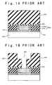
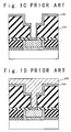
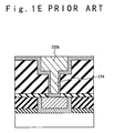
- Figs. 1A to 1E are cross section views showing the wiring line structure formed by a method forming of the connection plug and the wiring line by the dual damascene method.
- Fig. 1A is a cross sectional view showing a state in which a first copper containing metal wiring line 220a has been formed.
- a first silicon nitride film 212 and a first silicon oxide film 214 are formed on a semiconductor substrate 210 on which devices such as a transistor are formed.
- a wiring line groove is formed in the first silicon nitride film 212 and the first silicon oxide film 214 by a dry etching.
- a barrier metal film 216a and a copper film 218a are formed in this order to fill the wiring line groove. Subsequently, the surface of the substrate is flattened by a CMP method. Thus, the first copper containing metal wiring line 220a is formed. Subsequently, a second silicon nitride film 222 and a second silicon oxide film 224 are formed. In this way, the state of Fig. 1A is achieved.
- a connection hole 226 for a connection plug and a wiring line groove 228 are formed in a second silicon oxide film 224 by a lithography method and an etching method. Subsequently, an etching gas is changed and the etching of a second silicon nitride film 222 is carried out. Subsequently, as shown in Fig. 1C, the barrier metal film 230 is formed on the whole of second silicon oxide film 224 having the connection hole 226 and the wiring line groove 228.
- a copper film 232 is formed on the barrier metal film 230 and fills the connection hole 226 and the wiring line groove 228.
- connection plug 234 and a second copper containing metal wiring line 220b are formed.
- the semiconductor device is formed to contain a multiple wiring line structure.
- an object of the present invention is to improve the production yield of a semiconductor device with a copper containing metal wiring line structure.
- Another object of the present invention is to extend the lifetime of a semiconductor device with a copper containing metal wiring line structure.
- Still another object of the present invention is to increase the reliability of a semiconductor device.
- a method of manufacturing a semiconductor device is achieved by forming a first wiring line composed of a copper containing metal film on or above a semiconductor substrate; by forming a first interlayer insulating film on a whole surface of the semiconductor substrate to cover the first wiring line; by selectively removing the first interlayer insulating film to form a connection hole reaching the first wiring line; by forming a barrier metal film to cover an inner surface of the connection hole and then forming a copper containing metal film to fill the connection hole; by removing the copper containing metal film formed outside the connection hole; by forming a second interlayer insulating film on a whole surface of the semiconductor substrate to cover the copper containing metal film formed in the connection hole; by selectively removing the second interlayer insulating film to form a wiring line groove such that the copper containing metal film formed in the connection hole is exposed at a bottom; by forming a barrier metal film to cover an inside of the wiring line groove and then forming a copper containing metal film to fill the wiring line
- the manufacturing method of a semiconductor device may further include: changing a surface portion of the first wiring line into an amorphous layer before the step of forming the first interlayer insulating film. Also, the manufacturing method of a semiconductor device may further include siliciding a surface layer of the first wiring line before the step of forming the first interlayer insulating film.
- the manufacturing method of a semiconductor device may further include: cleaning the surface portion of the first wiring line before the step of forming the connection plug after the step of forming the first wiring line.
- the copper containing metal film of the first wiring line may be formed by a plating method.
- the insulating film may include ladder-type siloxane hydride.
- the manufacturing method of a semiconductor device may further include: forming a diffusion preventing film composed of SiC, SiCN, SiN or SiOC on the first wiring line before the step of forming the insulating film.
- the step of forming the connection hole may include the step of: selectively removing the first interlayer insulating film and the diffusion preventing film to form the connection hole.
- the step of forming the first wiring line may be achieved by forming the first copper containing metal film by a plating method; by forming a second copper containing metal film by a sputtering method on a surface of the semiconductor substrate to cover the first copper containing metal film; and by carrying out thermal treatment to the first copper containing metal film and the second copper containing metal film.
- a manufacturing method of a semiconductor device may be achieved by forming an insulating film on a semiconductor substrate and then forming a first wiring line composed of a copper containing metal film in the insulating film; by changing a surface portion of the first wiring line into an amorphous layer; and by forming a connection plug connected with the first wiring line and a second wiring line connected with the connection plug on the first wiring line, the connection plug and the second wiring line being composed of a copper containing metal film.
- a manufacturing method of a semiconductor device may be achieved by forming an insulating film on a semiconductor substrate and then forming a first wiring line composed of a copper containing metal film in the insulating film; by siliciding a surface portion of the first wiring line; and by forming a connection plug connected with the first wiring line and a second wiring line connected with the connection plug on the first wiring line, the connection plug and the second wiring line being composed of a copper containing metal film.
- the step of siliciding a surface layer of the first wiring line may include the step of: exposing the surface portion of the first wiring line to a gas containing silicon in a state of no plasma.
- the manufacturing method of a semiconductor device may further include: cleaning the surface portion of the first wiring line before the step of forming the connection plug after the step of forming the first wiring line.
- the step of cleaning the surface portion of the first wiring line may include the step of: rinsing the surface portion of the first wiring line with liquid containing carboxylic acid or the salt.
- the carboxylic acid may contain at least one selected from the group consisting of oxalic acid, citric acid, malic acid, maleic acid, succinic acid, tartaric acid or malonic acid.
- the step of cleaning the surface portion of the first wiring line may include the step of: processing the surface portion of the first wiring line with anti-corrosion agent containing benzotriazole or benzotriazole derivative.
- the step of cleaning the surface portion of the first wiring line may include the step of: carrying out a plasma process to the first wiring line.
- the step of cleaning the surface portion of the first wiring line may include the step of: carrying out the plasma process to the first wiring line in a deoxidization atmosphere.
- the copper containing metal film of the first wiring line may be formed by a plating method.
- the insulating film includes ladder-type siloxane hydride.
- the ladder-type siloxane hydride may contain L-Ox.
- the forming the insulating film may include the step of: sintering the insulating film in an atmosphere temperature in a range of 200 to 400 °C.
- the manufacturing method of a semiconductor device may further include: forming a diffusion preventing film composed of SiC, SiCN, SiN or SiOC on the first wiring line before the step of forming the insulating film.
- the step of forming the connection hole may include the step of: selectively removing the first interlayer insulating film and the diffusion preventing film to form the connection hole.
- the diffusion preventing film may be SiCN film.
- the step of forming the first wiring line may include the steps of: forming the first copper containing metal film by a plating method; forming a second copper containing metal film by a sputtering method on a surface of the semiconductor substrate to cover the first copper containing metal film; and carrying out thermal treatment to the first copper containing metal film and the second copper containing metal film.
- a manufacturing method of a semiconductor device may be achieved by forming on a semiconductor substrate, a copper containing metal film to have substantially uniform plane orientation at a surface of the copper containing metal film; and by forming a different kind element containing film containing a different kind element which is different from copper on the surface of the copper containing metal film.
- a manufacturing method of a semiconductor device may be achieved by forming a copper containing metal film on a semiconductor substrate having by a plating method to have an average grain size equal to or larger than 1 ⁇ m; and by forming a different kind element containing film containing a different kind element which is different from copper on the surface of the copper containing metal film.
- the step of forming the copper containing metal film may include the steps of: forming a first copper containing metal film on the semiconductor substrate; forming a second copper containing metal film by a sputtering method on the semiconductor substrate to cover the first copper containing metal film; and carrying out thermal treatment to the first copper containing metal film and the second copper containing metal film.
- the manufacturing method of the semiconductor device may further include: forming an insulating film on the semiconductor substrate; and forming a concave section in the insulating film.
- the step of forming the first metal film may be achieved by forming the first copper containing metal film to fill a part of the concave section
- the step of forming the second copper containing metal film may be achieved by forming the second copper containing metal film to fill a remaining part of the concave section.
- the step of forming the copper containing metal film may be achieved by removing the first copper containing metal film and the second copper containing metal film outside the concave section.
- the concave section may be a wiring line groove and the copper containing metal film forms a wiring line.
- the second copper containing metal film may be formed by a bias sputtering method in which a bias is applied to the semiconductor substrate.
- the step of forming the second copper containing metal film may be achieved by forming the second copper containing metal film such that a film thickness of the second copper containing metal film in a flat portion is thicker than a film thickness of the first copper containing metal film in the flat portion.
- the different kind element may be silicon
- the step of forming the different kind element containing film may be achieved by siliciding a surface portion of the copper containing metal film.
- the step of forming the different kind element containing film may be achieved by forming an alloy of copper and the different kind element on the surface of the copper containing metal film.
- the step of forming the different kind element containing film may be achieved by converting a surface portion of the copper containing metal film into an amorphous layer.
- the step of forming the copper containing metal film may be achieved by forming the copper containing metal film such that a plane orientation in the surface of the copper containing metal film is (200).
- a semiconductor device include: a semiconductor substrate; a first wiring line provided into an insulating film on the semiconductor substrate and formed of a copper containing metal film; a connection plug formed of a copper containing metal film, and connected with the first wiring line; and a second wiring line formed of the copper containing metal film, and connected with the connection plug.
- the surface portion of the first wiring line is an amorphous layer.
- a semiconductor device include: a semiconductor substrate; a first wiring line provided in a insulating film on the semiconductor substrate and formed of a copper containing metal film; a connection plug formed of a copper containing metal film, and connected with the first wiring line; and a second wiring line formed of the copper containing metal film, and connected with the connection plug.
- the surface portion of the first wiring line is a silicide layer.
- a semiconductor device include: a semiconductor substrate; a first wiring line provided in an insulating film on the semiconductor substrate and formed of a copper containing metal film; an interlayer insulating film formed on the first wiring line; a connection plug formed of the copper containing metal film, and connected with the first wiring line; and a second wiring line formed by laminating a barrier metal film and a copper containing metal film in this order, and connected with the connection plug.
- the surface portion of the first wiring line may be an amorphous layer.
- the surface portion of the first wiring line may be a silicide layer.
- the insulating film may contain ladder-type siloxane hydride.
- the ladder-type siloxane hydride may contain L-Ox.
- the insulating film is sintered at a temperature from 200 °C to 400 °C.
- the copper containing metal film of the first wiring line may be formed by a plating method.
- a plane orientation of the surface of the copper containing metal film which of the first wiring line may be substantially uniform.
- a semiconductor device include: a semiconductor substrate; a copper containing metal film formed on the semiconductor substrate to substantially uniform plane orientation in a surface of the copper containing metal film; and a different kind element containing conductive film formed of different kind element from copper on the surface of the copper containing metal film.
- a semiconductor device include: a semiconductor substrate; a copper containing metal film formed on the semiconductor substrate to have an average grain size equal to or more than 1 ⁇ m; and a different kind element containing conductive film formed of a different kind element from copper on the surface of the copper containing metal film.
- a semiconductor device in another aspect of the present invention, includes a semiconductor substrate; a copper containing metal film formed on the semiconductor substrate; and a different kind element containing conductive film formed on the surface of the copper containing metal film and containing a different kind element from copper.
- An average grain size of crystal of the copper containing metal film is larger than an average film thickness of the copper containing metal film.
- the different kind element may be silicon, and the different kind element containing film may be a silicide layer.
- the different kind element containing film may be formed of an alloy of the different kind element and copper.
- the different kind element containing film may be an amorphous layer.
- the plane orientation of the surface of the copper containing metal film may be (200).
- the copper containing metal film may function a wiring line, a plug or a pad.
- a metal wiring line formed of a copper containing plating film, contains a different kind element containing conductive film formed on the surface of the copper containing plating film and containing a different kind element from copper.
- An average size of grains contained in the copper containing plating film is equal to or more than 1 ⁇ m.
- a metal wiring line formed a copper containing plating film, contains a different kind element containing conductive film formed on the surface of the copper containing plating film and containing a different kind element from copper.
- the copper containing plating film is formed of a single grain.
- a width of the metal wiring line is equal to or more than 1 ⁇ m.
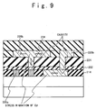
- the inventors of the present invention examined the causes that the production yield of the semiconductor device with the copper containing metal wiring line formed by the dual damascene method is low. As a result, the inventors found that a cavity was generated between a connection plug and a copper containing metal wiring line under the connection plug as shown in Fig. 9. The following two causes of the cavity generation could be considered.
- connection plug 234 was sucked up by the second copper containing metal wiring line 220b and the cavity was generated in the second silicon nitride film 222 and the second silicon oxide film 224.
- the cavity was generated in the first copper containing metal wiring line 220a around a lower portion of the connection plug 234.
- the cavity in the first copper containing metal wiring line 220a was easy to be generated in the wiring line, especially, when the width of the connection plug was about 1 to 12 ⁇ m. Also, the fact was found that such a cavity generation phenomenon occurs conspicuously at about 150 °C, which was a practical use temperature in the manufacturing processes of the semiconductor device such as a bonding process, and a baking process of the photo-resist.
- the cavity causes a connection defect between the connection plug and the wiring line, the decrease of the production yield of the semiconductor device and an unstable operation of the semiconductor device as the result of a long-term use.
- Fig. 10 is a diagram showing one of the causes that the cavity is generated.
- Fig. 10 shows the stress which is added to copper when a copper film is heated.
- the horizontal axis of Fig. 12 shows temperature and the vertical axis shows stress.
- the stress applied to the copper film changed from a stiffness mode into a compression mode at about 150 °C.
- the inventors supposed that the stress migration was caused in the copper containing metal in the connection plug and the wiring line to generate a cavity, when the change of such a stress mode has occurred. Especially, the inventors supposed that such a stress migration was promoted at the interfaces between the connection plug and the wiring line to generate a cavity.
- the inventors led the present invention based on the above suppositions to restrain the stress migration in the interfaces between the connection plug and the wiring lines.
- the copper containing metal may be metal which contains copper equal to or more than 30%.
- the copper containing metal may contain gold, silver, platinum and so on.
- the copper containing metal may contain chrome and molybdenum.
- Fig. 11 is a transmission-type electron microscope (TEM) photograph of a semiconductor device after the wiring ling structure was formed by such a single damascene method and the semiconductor device was located for 500 hours in the circumstance of about 150 °C.
- TEM transmission-type electron microscope
- Fig. 12 is a schematic plane view showing the cavity shown in Fig. 11.
- the cavity 302 was generated around the lower portion of the connection plug, when the connection plug was formed in the neighborhood of a boundary (301a) between particles or grains in the first wiring line surface.
- the connection plug was formed in a part (301b) which was not a boundary
- the cavity was difficult to be generated around the lower portion of the connection plug.
- the cavity was generated not directly below the connection plug but in the boundary.
- the cavity was easy to be generated in a region where the boundaries of the plurality of grains overlap complicatedly. From these results, the inventors found that it was one cause of the generation of the cavity that the stress migration was easy to be caused in the boundary portion in the first wiring line, especially, when the boundary exists in the neighborhood of the interface with the connection plug.
- an amorphous layer may be provided on the surface portion of the first wiring line.
- a halo pattern is confirmed in the refraction of an electron beam.
- a silicide layer may be provided on the surface portion of the first wiring line.
- the stress migration from the first wiring line can be reduced. Therefore, it is possible to prevent the generation of a cavity between the first wiring line and the connection plug.
- the cavity 302 is easy to be generated in the boundary of the grains.
- the cavity generation phenomenon is especially conspicuous when the copper containing metal film is formed by a plating method.
- the boundaries are generated between the grains when the copper containing metal film of the first wiring line is formed by the plating method. Therefore, it becomes easy for the cavity to be generated.
- the plane orientation in the copper surface differs for every grain such as (111) and (511), and the copper containing metal film surface with various plane orientations is exposed. This causes cavities.
- the semiconductor device can be stably manufactured.
- the copper containing metal film of the connection plug and/or the copper containing metal film of the second wiring line may be formed by the plating method.
- the copper containing metal film of the connection plug is formed by the plating method, it is easy for the boundaries between the grains to be generated. As a result, the semiconductor device is easy to receive the stress migration. In the manufacturing method of the present invention, the generation of a cavity between the first wiring line and the connection plug can be prevented.
- the silicide layer may be provided on the first wiring line.
- an oxide film exists on the copper containing metal film of the first wiring line, it is difficult to form the silicide layer in a region where the oxide film is formed.
- the thickness of the silicide layer is not uniform.
- the first wiring line is formed by the plating method, the plane orientation in the surface of the copper containing metal film is different, as mentioned above. In this case, the oxide film is formed ununiformly in thickness on the surface, because the easiness of the oxidation of the surface is different for every plane orientation. As a result, the metal silicide layer cannot have a uniform thickness.
- the thickness of the silicide layer is thick.
- the thickness of the silicide layer is thin. Therefore, it is important to control the thickness of the silicide layer to an appropriate thickness such that the above both conditions are met, in order to increase the production yield of the semiconductor device with a copper containing metal wiring line.
- the oxide film with un-uniform thickness has been formed on the copper containing metal film, it is difficult to control the thickness of the silicide layer. Therefore, the process of removing the oxide film from the copper containing metal film surface is important.
- a process is used which the surface portion of the first wiring line is cleaned.
- the oxidation of the copper containing metal film surface can be prevented and the oxide film such as an already formed CuOx film can be removed.
- the surface of the copper containing metal film can be uniformly silicided. Also, the performance of the semiconductor device can be improved.
- the surface portion of the first wiring line may be rinsed with a rinse liquid containing carboxylic acid or the salt.
- the carboxylic acid may contain at least one of oxalic acid, citric acid, malic acid, maleic acid, succinic acid, tartaric acid or malonic acid. Of the acids, the oxalic acid is especially preferable.
- the oxalic acid can efficiently remove the CuOx film due to the chelate operation. In this way, the copper containing metal film surface can be uniformly silicided.
- the surface portion of the first wiring line may be processed with anti-corrosion agent containing benzotriazole or benzotriazole derivative.
- the process of the anti-corrosion agent may be carried out immediately after a CMP process to the copper containing metal film in the first wiring line.
- the copper containing metal film surface can be protected from oxidixation and the copper containing metal film can be uniformly silicided.
- the copper containing metal film surface may be rinsed and then the process of the anti-corrosion agent may be carried out.
- oxide films such as the CuOx film can be removed and a new oxide film can be prevented in the copper containing metal film of the first wiring line.
- the cleaning process may be achieved by carrying out a plasma process to the first wiring line under the deoxidizing atmosphere.
- the anti-corrosion agent can be volatilized.
- the oxide film such as the CuOx film formed on the copper containing metal film surface can be removed.
- the copper containing metal film surface can be uniformly silicided.
- the anti-corrosion agent can be volatilized from the copper containing metal film surface. This process may be carried out after the process of siliciding the surface portion of the first wiring line. Even if silicon is deposited on the insulating film of the semiconductor device during the siliciding process, silicon is nitrided to prevent a short-circuit between wiring lines by carrying out the process as an ammonia plasma process.
- the method of siliciding the surface of the copper wiring line is described in Japanese Patent No. 2,809,196, Japanese Laid Open Patent Application (JP-A-Heisei 9-255687), and Japanese Laid Open Patent Application (JP-P2000-150517A), for example.
- JP-A-Heisei 9-255687 Japanese Laid Open Patent Application
- JP-P2000-150517A Japanese Laid Open Patent Application
- the technique is described that a silicide layer is formed on the surface portion of the copper wiring line for prevention the oxidation of the copper wiring line.
- the miniaturization of the copper wiring line is being advanced. For this reason, the increase of the contact resistance when the silicide layer is formed on the copper wiring line is focused as a new problem.
- the film thickness of the silicide layer cannot be appropriately controlled, a relative thickness of the silicide layer to the whole film thickness of the copper wiring line increases. Therefore, in the semiconductor device with the multiple wiring line structure which a copper wiring line and a connection plug are stacked, various processes are carried out rather to suppress the forming of the silicide layer.
- a method of controlling a silicide layer thickness is described in USP 6,181,013 and USP 6,211,084.
- SiH 4 plasma is generated to try to control the forming a silicide layer on the copper surface before the oxidation prevention film such as SiN is formed.
- a polysilicon film is formed in a region other than the copper surface. Therefore, there is a risk that a short-circuit is formed between the wiring lines. This point will be described later.
- the forming of a silicide layer is demanded to reduce the stress migration in the semiconductor device containing a connection plug and a wiring line which are composed of a copper containing metal film.
- the copper containing metal wiring line is formed by a plating method, it is important to form the silicide layer with an appropriate film thickness, because the generation of the boundaries of the grains is inevitable.
- an oxide film can be removed from the surface of the copper containing metal film of the first wiring line by a cleaning process of the surface portion of the first wiring line. Also, especially, the forming of a further oxide film can be prevented by the processing of using an anti-corrosion agent. Therefore, it is possible to control the thickness of the silicide layer appropriately in the copper containing metal wiring line film. In this way, in the semiconductor device having a multiple wiring line structure, it is possible to suppress the influence of the contact resistance and to reduce the stress migration, resulting in the increase in the reliability of the device.
- the copper containing metal wiring line film with the substantially uniform plane orientation is formed.
- the substantial uniformity of the plane orientation means that grains equal to or more than 70% at least in the copper containing metal have the same plane orientation as the result of an X-ray analysis method.
- the different kind element may contain one or more selected from the group consisting of Si, Ag, W, Mg, Be, Zn, Pd, Cd, Au, Hg, Pt, Zr, Ti and Sn.
- Si is used as the different kind element
- the copper containing metal film surface can be silicided and can improve the stress migration endurance of the copper containing metal film.
- the different kind element containing film may be formed as an alloy of copper and the different kind element. In this case, it is possible to improve the strength. Also, it is possible to protect the surface of the copper containing metal film and to reduce the stress migration of the copper containing metal film.
- the resistance increase of the copper containing metal film can be suppressed.
- Zr or Ti is used as the different kind element, it is possible to improve the fitness between the copper containing metal film and the insulating film and the barrier metal film.
- Mg is used as the different kind element, it is possible to prevent the corrosion of the copper containing metal film surface.
- the average size of the grains in the copper containing metal film is equal to or more than 1 ⁇ m, the boundaries of the grains in the copper containing metal film surface can be reduced.
- the grain size is calculated as an average of the length in a longer axis and the length in a shorter axis of each grain.
- the average grain size is an average of the grain sizes.
- a bias sputtering method can be carried out by applying RF (high frequency) bias or a DC (direct current) bias to the semiconductor substrate.
- ion irradiation energy (plasma potential + self bias), which is applied to the semiconductor substrate, is a high bias, e.g., 80 eV or more, preferably, 200 eV or more.
- the plane orientation of the copper containing metal film can be made substantially uniform through a subsequent thermal treatment. Also, it is possible to make the average grain size of these copper containing metal film can equal to or more than 1 ⁇ m.
- the step of forming a different kind element containing film may include a step of forming an alloy of copper and different kind element on the surface of the copper containing metal film.
- alloy in this specification means one obtained by melting two or more metal elements and solidifying it, and may contain a nonmetal or metalloid element in addition to the metal element.
- the structure state of alloy there are a case of solid solution, a case of intermetallic compound and a case of mixture of them, based on the mixture of elements. That is, a substance in which the element is added more than a solid solution limit is also referred to as "alloy".
- the grain size is small, compared with the wiring line width and the boundaries of a lot of grains existed in the copper film surface.
- the grain size can be made large. Therefore, the number of boundaries of the grains in the copper containing metal film surface can be reduced. Thus, it is possible to improve in the wiring line stress migration endurance.
- the barrier metal film in the present invention contains refractory metal such as Ti, W and Ta.
- refractory metal such as Ti, W and Ta.
- films of material such as Ti, TiN, W, WN, Ta and TaN are exemplified.
- a tantalum-based barrier metal is preferably used and in which a TaN film and a Ta film are laminated.
- the barrier metal film can be formed by various methods such as a sputtering method, a CVD method.
- Amorphous metal in the present invention is Cu silicide.
- the Cu silicide is formed by siliciding the surface of the copper containing metal film.
- the siliciding is carried out by exposing the surface of the copper containing metal film to a gas containing silicon.
- a gas containing silicon a gas obtained by diluting monosilane, disilane, trisilane or tetrasilane with inert gas such as nitrogen gas is used.
- the rate of the siliciding can be reduced so that the film thickness of the silicide layer can be controlled to a preferable thickness.
- an average film thickness of the silicide layer can be made equal to or more than 5 nm.
- the stress migration to the first wiring line can be reduced.
- the upper limit of the average film thickness of the silicide layer can be made equal to or less than 30 nm.
- the stress migration to the first wiring line can be reduced.
- the high performance semiconductor device can be manufactured in a high production yield without undergoing influence of contact resistance between a connection plug and the first wiring line.
- the siliciding may be carried out by an ion implantation.
- the boundaries in the first wiring line surface can be made discrete.
- an anti-corrosion processing of the copper containing metal film surface by an anti-corrosion agent a plasma process method under a deoxidizing atmosphere or a rinsing method of the copper containing metal film surface with a rinsing liquid are exemplified.
- benzotriazole (BTA) and benzotriazole derivative can be used as the anti-corrosion agent in the present invention.
- the anti-corrosion agent is generally solution in which the concentration of BTA or the derivative is equal to or less than 3%.
- a soluble compound which does not contain a metal atom in molecule and contains one or more nitrogen atom the concentration of BTA or the derivative can be made more than 3%.
- ammonium hydroxide, tetramethylammonium hydroxide, amin compound and amide compound and so on can be given.
- heterocyclic compound has the six-fold-ring containing nitrogen atom in the molecule can be used as the anti-corrosion agent.
- Such a heterocyclic compound shows good anti-corrosion operation due to the chelate operation of the nitrogen atom in the complex ring, and has good biodegradation property.
- heterocyclic compound purine and the derivative such as purine, 6-aminopurine, 2-amino-6-oxopurine, 6-furfurylaminopurine, 2,6-(1H. 3H)-purinedione, 2-amino-6-hydroxy-8-mercaptpurine, allopurinol, uric acid, kinetin, zeatin, guanine, xanthine, hypozanthine, adenine, theophylline, caffeine, and theobromine; azaguanine and the derivative such as 8-azaguanine; pteridine and pterin and the derivatives of them such as pteridine, pterin, 2-amino-4,6-dihydroxypteridine, 2-amino-4,7-dihydroxypteridine, and 2-amino-4,6,7-trihydroxypteridine; cyanuric acid and isocyanuric acid and the derivatives of them such as tris
- purine and the derivative may be used individually and tow or more.
- cyanuric acid and isocyanuric acid and the derivatives; and nicotine acid and the derivative are preferably used. It is because they shows the excellent anti-corrosion effect to metals such as copper and has good biodegradation property.
- purine and the derivative never inflict damage on a semiconductor substrate and various films formed on it and show the excellent anti-corrosion effect to metals such as copper. Therefore, it is preferably used.
- the compound shown by the following general equation (1) i.e., uric acid is naturally widely distributed and has the high safety. Also, uric acid has excellent biodegradation property, the conspicuously excellent anti-corrosion and it is preferably used.
- A1, A2 and A3 independently show a hydrogen atom, a hydroxyl base, and alkyl base or amino base with carbons of 1 to 5, respectively
- the compound has the structure which has amide combination in the complex annulus, and the good anti-corrosion operation and biodegradation.
- an ammonia plasma process can be used as the plasma process under a deoxidizing atmosphere.
- the oxide on the wiring line copper containing metal film surface can be deoxidized.
- BTA is used as the anti-corrosion agent, it is difficult for BTA to be removed, but BTA can be removed through evaporation by carrying out the plasma process immediately before the siliciding process.
- the rinsing liquid in the present invention can contain carboxylic acid or the salt.
- the carboxylic acid may contain oxalic acid, citric acid, malic acid, maleic acid, succinic acid, tartaric acid or malonic acid.
- the insulating film is a film containing ladder-type oxide such as ladder-type siloxane hydride.
- ladder-type siloxane hydride film or a laminate film of film of the ladder-type siloxane hydride film and a SiO 2 film is desirable.
- the ladder-type siloxane hydride is a polymer which has a ladder-type molecule structure.
- the dielectric constant is 2.9 or below preferably from the viewpoint of the wiring line delay prevention, and also the low film density is desirable.
- the film density is from 1.50 g/cm 3 to 1.58 g/cm 3 and the refractive index at the wavelength of 633 nm is from 1.38 to 1.40.
- L-Ox can be exemplified.
- Fig. 19 shows the structure of L-Ox (trade mark) which has ladder-type siloxane hydride structure.
- n is a positive number equal to or more than 1.
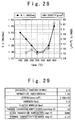
- Fig. 29 shows the physical data of L-Ox with such a structure.
- L-Ox has the structure of Fig. 19. It was the sharp spectrum of a Si-H combination which appeared in about 830 cm -1 that was characteristic in the chart of Fig. 20. The steepness of this spectrum suggests that L-Ox has a 2-dimension structure. Also, the spectrum of another Si-H combination appeared near 870cm -1 in the higher wave number side with extremely small peak. This fact would show that the measurement object material has the 2-dimension structure.
- the L-Ox When being sintered in a range of 200 C to 400 C in the atmosphere of inert gas such as nitrogen, the L-Ox has following characteristic.
- R.I. shows refractive index at the wavelength of 633 nm.
- the refractive index is a parameter which directly influences dielectric constant, and this value changes between 1.38 to 1.40.
- the value exceeds 1.40 when the sintering temperature is less than 200 C or is higher than 400 C.
- the density of the L-Ox which is sintered in the range of 200 C to 400 C is 1.50 to 1.58 g/cm 3 .
- the density exceeds 1.60 g/cm 3 in case of the sintering temperature over 400 C, and the density could not be measured in case of the sintering temperature less than 200 C.
- L-Ox with a low dielectric constant characteristic can be stably obtained through the sintering process in the temperature range of 200 C to 400 C when an insulating film containing the L-Ox is formed.
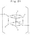
- Fig. 21 shows the molecule skeleton of HSQ (Hydrogen Silsesquioxane) with the hydrogen Silsesquioxane structure and 3-dimentional structure which are conventionally known (Semiconductor Technology Outlook, 1998, pp. 431-435).
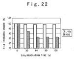
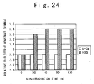
- the materials of the two structures are different from each other in the film stability in the manufacture process and the L-Ox is conspicuously excellent. This could be considered that the decreasing amount of Si-H is less in the L-Ox, compared with HSQ. Also, it could be considered as one of the causes that that the state of the combination of hydrogen atom in the insulating film is different. That is, in HSQ, a hydrogen atom is combined in the corner of the solid structure, whereas in L-Ox a hydrogen atom is combined with the side of the ladder structure. Therefore, it could be considered that the density of the neighborhood of the hydrogen atom is lower and the hydrogen combination in HSQ becomes the structure which is wealthy in the reactivity than L-Ox about HSQ.
- the difference in the film stability between HSQ and L-Ox will be described later with reference to the embodiments.
- various films can be used as the diffusion prevention film.
- sic, SiCN, SiOC, or siON are used.
- the material of such a low dielectric constant the capacity between the wiring lines can be reduced.
- Figs. 27A and 27B shows examples of a sequence of gas and RF power.
- the flowed gas is SiH4, NH3, or N2.
- the flowed gas is trimethylsilane (hereinafter, are 3MS), SiH 4 , NH 3 , and N 2 .
- N 2 is flowed without the application of RF power, and the oxidation protection film (e.g., BTA) in the wiring line surface is desorbed with heater heat.
- SiH 4 is introduced to form a silicide layer on the Cu surface.
- NH 3 is introduced to form a SiN film.
- SiH 4 and NH 3 are introduced at the same time and the gases are stabilized.
- SiH 4 resolves on the Cu wiring line surface and a silicide layer becomes thicker excessively so that the deviation of the wiring line layer resistance becomes large.
- N 2 is first flowed without the application of RF power, like SiN, and the oxidation protection film (e.g., BTA) on the wiring line surface is desorbed with the heater heat.
- the oxidation protection film e.g., BTA
- SiH 4 is introduced and a silicide layer is formed on the Cu surface.
- the SiH 4 gas is stopped and 3MS and NH3 gas are introduced and then the step of the gas stabilization is started.
- 3MS is not resolved on the Cu surface, the unnecessary silicide layer is not formed unlike the case of the SiN and it is possible to suppress the deviation of the wiring line layer resistance.
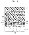
- Fig. 2 is a cross sectional view showing an example of the semiconductor device according to the present invention.
- a MOS transistor is formed to have a gate electrode 102, diffusion layers 104 on a silicon substrate 100.
- An insulating film 106 is formed to cover the MOS transistor.
- the copper connection plug s108 are formed in the insulating film 106 to connect with the diffusion layers 104 and a first copper wiring line 22a, a connection plug 28 and a second copper wiring line 22b are formed in order on the surface portion.
- a copper wiring line layer is formed to have the same or similar structure on the surface portion of the layer containing the copper wiring line, and a passivation film 114 is provided for the uppermost layer.
- first copper wiring line 22a is electrically connected with the device formed on the silicon substrate 100. Also, a set of the first copper wiring line 22a, the connection plug 28 and the second copper wiring line 22b to be described below may be provided for whichever layer of the semiconductor device shown in Fig. 2.
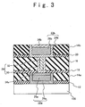
- Fig. 3 is a cross sectional view showing the wiring line structure in the first embodiment of the present invention.
- a first laminate layer 14a in which a first SiCN film 12, L-Ox film and a SiO 2 film are laminated in this order, and a second laminate layer 14b in which a second SiCN film 16, a silicon oxide film 18, a third SiCN film 20 and a L-Ox film and a SiO 2 film are laminated are laminated on an insulating film 106 on the silicon substrate (not shown).
- the first copper wiring line 22a and the second copper wiring line 22b are formed, respectively.
- the first copper wiring line 22a are formed of a tantalum-based barrier metal film 24a and a copper film 26a.
- a connection plug 28 is formed to connect with the surface of the first copper wiring line 22a.
- the connection plug 28 is formed of a tantalum-based barrier metal film 30 and a copper film 32.
- the second copper wiring line 22b is formed to connect with the surface of the connection hole.
- the second copper wiring line 22b is formed of a tantalum-based barrier metal film 24b and the copper film 26b.
- a first Cu silicide layer 34a is formed on the surface of the first copper wiring line 22a
- the second Cu silicide layer 34b is formed on the surface of the second copper wiring line 22b, respectively.
- Fig. 4A shows the structure in which a wiring line groove is formed in first SiCN film 12 and the first laminate layer 14a. This structure is formed by etching the first SiCN film 12 and the first laminate layer 14a step-by-step after the first SiCN film 12 and the first laminate layer 14a are formed and then a resist film (not shown) is patterned into a predetermined shape.
- the tantalum-based barrier metal film 24a is formed in which Ta and TaN are deposited on the substrate surface (the film thickness of about 20 nm for Ta, and the film thickness of about 10 nm for TaN) by a sputtering method and a reactivity sputtering method (Fig. 4B).
- the copper film 26a is formed on the tantalum-based barrier metal film 24a.
- the copper film 26a is formed as follows by a plating method. First, a seed copper film of copper is deposited by the sputtering method for growth of a copper plating film. Next, the substrate is immersed in copper sulfate solution with the liquid temperature of about 25 C so that the copper film 26a is formed by an electrolysis plating method (the film thickness of about 600 nm in a flat section).
- an annealing process is carried out to the substrate thus obtained, for about 30 minutes at 350 C.
- the particle diameter of a grain in the copper film 26a becomes large, compared with the particle diameter before the annealing process.
- a portion where a plurality of boundaries of the grains exposed in the surface of the copper film 26a overlap decreases relatively. Therefore, it becomes difficult for the cavity to be produced.
- the resistance value of the first copper wiring line 22a after such an annealing process decreases the resistance value thereof before the annealing process.
- the annealing process may be carried out in a temperature range of 200 C to 500 C.
- the unnecessary copper film 26a and the tantalum-based barrier metal film 24a which are formed outside the wiring line groove are removed by a chemical mechanical polish (CMP) method.
- CMP chemical mechanical polish
- the copper film 26a and so on are left inside the wiring line groove.
- the first copper wiring line 22a is formed (Fig. 4D).
- the anti-corrosion process is carried out in which the surface of the copper film 26a is processed by BTA as an anti-corrosion agent immediately after the CMP process to the copper film 26a.
- BTA as an anti-corrosion agent immediately after the CMP process to the copper film 26a.
- 0.05% BTA solution is used.
- the first Cu silicide layer 34a is formed on the surface of the copper film 26a of the first copper wiring line 22a.
- the method of forming the first Cu silicide layer 34a will be described below.
- SiH 4 is flowed for about 60 seconds (the flow rate of SiH 4 is 5000 sccm, while the flow rate of N 2 is 50 sccm) under the pressure of 3 torr at the temperature of 350 C.
- the surface of the copper film 26a is silicided.
- the first Cu silicide layer 34a with the thickness of about 10 nm is formed.
- the second SiCN film 16 (the film thickness of about 70 nm), the silicon oxide film 18 (the film thickness of about 350 nm) are formed (Fig. 4F).
- the silicon oxide film 18 is etched using a lithography method until the second SiCN film 16 is exposed. Subsequently, the etching gas is replaced and the second SiCN film 16 is etched until the surface of the first Cu silicide layer 34a is exposed. Thus, as shown in Fig. 4G, the connection hole 40 is formed.
- the tantalum-based barrier metal film 30 and the copper film 32 are formed in this order (Fig. 4H).
- the copper film 32 is formed by the plating method like the copper film 26a of the first copper wiring line 22a.
- a flattening process by the CMP is carried out and the connection plug 28 is formed (Fig. 4I).
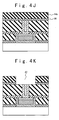
- the third SiCN film 20 (the film thickness of about 70 nm) and the second laminate layer 14b (the film thickness of about 300 nm) are formed on a surface portion of the connection plug 28 (Fig. 4J).
- the wiring line groove 42 is formed by a dry etching (Fig. 4K).
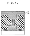
- the tantalum-based barrier metal film 24b and the copper film 26b are formed in this order (the film thickness of about 600 nm in the flat section) in order to fill the groove 42 (Fig. 4L).
- the copper film 26b is formed with the plating method like the copper film 26a of the first copper wiring line 22a.
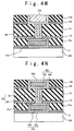
- the flattening process by the CMP process is carried out and the second copper wiring line 22b is formed (Fig. 4M).
- the anti-corrosion process to the copper film 26b by BTA is carried out.
- BTA is removed in the evaporation by the ammonia plasma process, a siliciding process is carried out and the second Cu silicide layer 34b is formed (Fig. 4N).
- the wiring line structure is formed as shown in Fig. 3.
- the semiconductor device By repeating the above-mentioned processes, it is possible to manufacture the semiconductor device with the multiple wiring line structure of 3 or more layers, as shown in Fig. 2.
- the second embodiment is different from the first embodiment in that BTA is evaporated and removed through a heating process at about 350 C instead of the ammonia plasma process, before the siliciding process of the surface of the copper film 26a and the surface of the copper film 26b.
- the heating process the wiring line structure shown in Fig. 3 is formed.
- the heating temperature at which BTA is evaporated and removed may be from 150 C to 450 C.
- the siliciding process can be carried out while BTA is removed. Therefore, it is possible to control the siliciding process such as a film thickness control of the Cu silicide. Also, by carrying out the heating process for the evaporation and removal of the BTA as in the second embodiment, the corrosion of the boundaries of the grains in the surface of the copper film 26a or the surface of the copper film 26b by gas such as ammonia can be prevented. Therefore, the good wiring line structure can be formed.
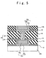
- Fig. 5 is a diagram showing the wiring line structure in the third embodiment.
- the third embodiment is different from the first embodiment in that the first Cu silicide layer 34a and the second Cu silicide layer 34b are not formed, and that the BTA anti-corrosion processing is not carried out.
- the description of the same components of Fig. 5 as those of Fig. 3 will be omitted by allocating the same reference numerals.
- the processes are carried out as in the first embodiment until the CMP process to the copper film 26a of the first copper wiring line 22a process. Subsequently, the second SiCN film 16 and the silicon oxide film 18 are formed without carrying out the siliciding process of the surface of the copper film 26a. Before the second SiCN film 16 is formed, a surface treat process of the copper film 26a of the first copper wiring line 22a is carried out by the ammonia plasma process. The process after the silicon oxide film 18 is formed is also the same as the first embodiment.
- the wiring line structure shown in Fig. 5 is formed through the above processes.
- the fourth embodiment is different from the third embodiment in that BTA anti-corrosion processing is carried out immediately after the CMP process to the surface of the copper film 26a or the surface of the copper film 26. Subsequently, before forming of second SiCN film 16, a surface treating of the copper film 26a of the first copper wiring line 22a is carried out by the ammonia plasma process. The wiring line structure similar to that shown in Fig. 5 is formed through this process. In this way, the surfaces of the copper films 26a and 26b can be protected by the BTA anti-corrosion process immediately after the CMP process. Therefore, the 'reliability of the semiconductor device containing such a copper wiring line can be increased through the anti-corrosion operation to on the copper film surfaces.
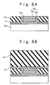
- Figs. 6A to 6F are cross sectional views showing the wiring line structure manufacturing process in the fifth embodiment.
- the fifth embodiment is different from the first embodiment in that the connection plug 28 and the second copper wiring line 22b are formed by the dual damascene method.
- the same components of Figs. 6A to 6F as those of Fig. 3 are allocated the same reference numerals, and the description will be omitted.
- the first copper wiring line 22a is formed as in the first embodiment described with reference to Figs. 4A to 4N. Then, the first Cu silicide layer 34a is formed on the surface of the copper film 26a (Fig. 6A).
- a connection hole 52 for the connection plug 28 and a wiring line groove 54 are formed in the silicon oxide film 50 by a step-by-step etching method using a lithography method. Subsequently, the etching gas is changed and the etching of the second SiCN film 16 is carried out. Subsequently, as shown in Fig. 6D, the tantalum-based barrier metal film 56 is formed on the whole surface of the silicon oxide film 50 containing the connection hole 52 and the wiring line groove 54. The tantalum-based barrier metal film 56 is formed of a Ta film and a TaN film.
- a copper film 58 is formed on the tantalum-based barrier metal film 56 to fill the connection hole 52 and the wiring line groove 54.
- a CMP flattening process is carried out to remove the copper film 58 and the tantalum-based barrier metal film 56 from a portion other than the wiring line groove 54.
- the connection plug 28 and the second copper wiring line 22b are formed.
- the BTA anti-corrosion process is carried out.
- the BTA is evaporated and removed by the ammonia plasma process, a siliciding process is carried out.
- the second Cu silicide layer 34b is formed (Fig. 6F).
- the wiring line structure in the fifth embodiment is formed by above processes.
- 2-layer wiring line structures as shown in Fig. 7A are formed by the methods in the first to fifth embodiments to examine the production yields, respectively.
- the 2-layer wiring line structure is called a via-chain.
- the 10,000 first copper wiring lines 22a are provided in parallel and the 10,000 second copper wiring lines 22b are provided in parallel to be orthogonal to the first copper wiring lines. These wiring lines are connected by 20,000 connection plugs 28.
- the semiconductor substrate, an interlayer insulating film and so on are omitted.
- the current flows in the direction shown in Fig. 7B by the arrows.
- the 2-layer wiring line structures corresponding to the first to fifth embodiments are called the wiring line structures 1 to 5, respectively.
- the existence of CuSix was confirmed in the wiring line structures 1, 2 and 5 by the fluorescence X ray analysis.
- a comparison sample is formed in which the copper film 26a of the first copper wiring line 22a is formed, and the BTA anti-corrosion process and the ammonia plasma process are carried out, and then the connection plug 28 and the second copper wiring line 22b are formed by the dual damascene method without the siliciding process of the surface of the copper film 26a (Wiring line structure 6).
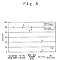
- the wiring line structure from 1 to 6 were located for 500 hours at the temperature of 150 C. Subsequently, the production yield examination of the via-chains was carried out. Also, a sample as a reference was prepared in which SiH 4 gas was flowed to form a silicide layer while generating plasma (Wiring line structure 7). The production yield of the via-chain was measured in the 2-layer wiring line structures (reference wiring line structure 1 and reference wiring line structure 2) which were formed like the wiring line structures 1 and the wiring line structure 5 and were left for 500 hours at the room temperature. The following table 1 shows the production yield (%) of each wiring line structure when it was supposed that the production yields in the reference wiring line structures 1 and 2 were 100% and the production yield in the wiring line structure 6 was 0%.
- Fig. 8 is a graph showing data of the production yield shown in table 1. As shown in Fig. 8, there is no difference between the single damascene method and the dual damascene method in the reference wiring line structures 1 and 2 which were left at the room temperature is not present. Also, the production yield is approximately 100% in the wiring line structure 1 and the wiring line structure 2 in which the BTA anti-corrosion process and the siliciding process are carried out and which are formed using the single damascene method.
- the production yield is 40% in the wiring line structure 4 which is formed using the single damascene method like the wiring line structure 1 and the siliciding process is not carried out. This value is less than a half of the production yield of the wiring line structure 1. It could be considered that this results from that the copper film 26a of the first copper wiring line 22a is protected by the first Cu silicide layer 34a, and a stress from the second copper wiring line 22b as an upper layer and connection plug 28 is relaxed so that the generation of the cavity in the first copper wiring line 22a can be prevented.
- the production yield is 90% in the wiring line structure 5 which is formed by the dual damascene method and in which the siliciding process is carried out. This production yield is greatly improved, compared with the wiring line structure 6 (production yield of 0%) in which the siliciding process is not carried out although it is formed using the dual damascene method. It could be considered that the increase of the production yield results from that the copper film 26a of the first copper wiring line 22a is protected by the first Cu silicide layer 34a, and a stress from the second copper wiring line 22b as an upper layer and connection plug 28 is relaxed so that the generation of the cavity in the first copper wiring line 22a can be prevented.
- the production yield is improved in the wiring line structure 1 formed using the single damascene method, compared with the wiring line structure 5 formed using the dual damascene method.
- the sucking-up of copper into the connection plug 28 occurs from the second copper wiring line 22b formed using the dual damascene method.
- a cavity is produced between the connection plug 28 and the first copper wiring line 22.
- the generation of such a cavity could be prevented.
- the production yield is 15% in the wiring line structure 3 in which neither of the BTA anti-corrosion process and the siliciding process are carried out. This value is improved, compared with the production yield in the wiring line structure 6 in which the BTA anti-corrosion process is carried out and is formed using the dual damascene method. From the above, it could be understood that the formation of the copper wiring line by the single damascene method results in the improvement of the production yield.
- the production yield is decreased by the difference in the production yield between the wiring line structure 5 and the wiring line structure 1 or more, in the wiring line structure 6 formed using the dual damascene method, compared with the wiring line structure 4 formed using the single damascene method. It could be considered that this results from that the sucking-up of copper by the second copper wiring line 22b happens from the first copper wiring line 22a in addition to the connection plug 28, so that the cavity is generated between the first copper wiring line 22a and the connection plug 28 when the surface of the copper film 26a of the first copper wiring line 22a is not protected by the first Cu silicide layer 34a.
- a leak current is measured between the wiring lines in each wiring line structure. The result is shown in Figs. 26A and 26B.
- the leak current is hardly present in the wiring line structures 1 to 6.
- the leak current is large in the wiring line structure 7 in which plasma is generated and the silicide layer is formed. This could be considered as the result that a polysilicon layer is formed on the wiring line insulating film and Cu atoms are diffused into the insulating film.
- the production yield can be increasingly improved by protecting the copper film 26a of the first copper wiring line 22a by the first Cu silicide layer 34a. Also, it is found that the production yield is greatly improved even if the second copper wiring line 22b is formed on the connection plug 28 provided on the first copper wiring line 22a and the surface peripheral portion of the connection plug 28 using the single damascene method. Also, it is found that the production yield further improved by the combination of the protection of the copper film 26a by the first Cu silicide layer 34a and the formation of the connection plug 28 and the second copper wiring line 22b using the single damascene method. Also, it is found that it is preferable from the prevention of leak between wiring lines that the silicide layer is formed without generating plasma.
- the production yield examination of the via-chain was carried out in the same way to the wiring line structure which was formed in the similar processes to the first, second and fifth embodiments and a process was added that the surface of the copper film 26a is rinsed with oxalic acid before the BTA anti-corrosion process after the CMP process to the copper film 26a of the first copper wiring line 22a.
- the result was equal to or better than the above-mentioned result. It could be considered that this results from that the chelate operation of the oxalic acid effectively removes a copper oxide (CuOx) film from the surface of the copper film 26a.
- CuOx copper oxide
- the seventh embodiment is different from the first embodiment or the second embodiment in a method of forming the first copper wiring line 22a and the second copper wiring line 22b.
- the tantalum-based barrier metal film 24a is formed in the wiring line groove.
- a seed copper film 60 (about 100 nm) is formed by a sputtering method on the tantalum-based barrier metal film 24a.
- a plating copper film 62 (the film thickness of about 150 nm in the flat section) is formed on the seed copper film 60 by the electrolysis plating method (Fig. 13A).
- the plating copper film 62 has (111) orientation. Also, it is assumed that the total film thickness of the seed copper film 60 and the plating copper film 62 is t1.
- a bias sputtering copper film 64 (the film thickness of about 900 nm in a flat section) is formed on the plating copper film 62 in the Cu sputtering chamber by a bias sputtering method without exposing the substrate to the atmosphere by applying a DC bias to the silicon substrate (Fig. 13B).
- the bias sputtering copper film 64 is formed while argon ions are irradiated to a sputtering growth surface.
- the ion irradiation energy applied to the silicon substrate is a high bias, e.g., 80 eV or more, preferably, 200 eV or more.
- the substrate temperature is set to -5 C.
- the bias sputtering copper film 64 is formed to have the film thickness t2 of the bias sputtering copper film 64 thicker than the above-mentioned t1. At this time, it is confirmed that the bias sputtering copper film 64 had (111) orientation.
- a heat treatment process is carried out for 30 minutes at 400 C in the inert gas atmosphere.
- the crystal orientation of the bias sputtering copper film 64, plating copper film 62 and seed copper film 60 changes to (200).
- a copper film 66 is formed to have the average grain size of the huge grains of hundreds of ⁇ m (Fig. 13C).
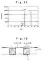
- Fig. 17 is a diagram showing the analysis result of the copper film 66 formed as mentioned above by the X-ray diffraction method. As shown in this figure, the grains of 93% (190468/204419) or more have plane orientation (200) in the copper film 66 surface. Also, when the grain size in the surface of the copper film 66 is confirmed by the optical microscope, most of the grains are larger than 100 to 200 ⁇ m, or more and some are larger than 500 ⁇ m.
- the unnecessary copper film 66 and the tantalum-based barrier metal film 24a formed outside the wiring line groove are removed by the CMP process such that only the copper film 66 and so on are left inside the wiring line groove.
- the first copper wiring line 22a is formed (Fig. 13D). A part of the samples is examined in this step. It could be confirmed that a 70% of the copper film 66 of the first copper wiring line 22a is formed with single grains.
- the wiring line width of the first copper wiring line 22a is 10 ⁇ m
- the length of the wiring line is 100 ⁇ m
- the film thickness is 300 nm.
- the surface process of the copper film 66 by BTA is carried out like the second embodiment, and the first Cu silicide layer 34a is formed after the BTA is evaporated and removed by the heating process of about 350 C.
- the connection plug 28 is formed like the first embodiment and the second embodiment.
- the second copper wiring line 22b is formed like the first copper wiring line 22a mentioned above in this embodiment.
- a bias sputtering copper film 64 is formed on the plating copper film 62, and then a heat-treating is carried out.
- the plane orientation of the crystal of copper can be controlled.
- the surface of copper film 66 can be uniformly kept, and the Cu silicide layer can be uniformly formed on the copper film 66. Therefore, the film thickness of the Cu silicide layer can be appropriately controlled, and while suppressing the resistance increase rate of the first copper wiring line 22a and the second copper wiring line 22b, these wiring lines can be protected.
- the grain size of copper can be made large through the above mentioned heat treatment process, the number of the boundaries of the grains in the copper film 66 surface can be substantially reduced.
- the stress migration endurance of the wiring line structure can be increased.
- the Cu silicide layer is formed in the surface of the copper film 66. Therefore, the displacement of the crystal of copper can be suppressed, and the stress migration endurance of the wiring line structure can be improved.
- the grain size of the copper film of the copper wiring line can be made large, the wiring line resistance can be reduced.
- the boundary of the grain is hardly generated in the surface of the copper film 66 in this embodiment, the Cu silicide can be uniformly formed from this viewpoint. It could be confirmed by an outward appearance test apparatus (KLA-Tencor) that the Cu silicide layer is formed uniformly in the wiring line surface in this embodiment.
- the eighth embodiment is different from the seventh embodiment in that a CVD copper film 68 is formed by a plasma CVD method instead of that the seed copper film 60 and plating copper film 62 when the first copper wiring line 22a and the second copper wiring line 22b are formed.
- the eighth embodiment will be described with reference to Figs. 14A to 14D.
- the CVD copper film 68 is formed by the plasma CVD method (the film thickness of about 200 nm in a flat section) (Fig. 14A).
- the crystal orientation of the CVD copper film 68 is (111).
- the copper oxide in the CVD copper film 68 surface is sputtered and reduced by the Ar/H 2 plasma with the room temperature in the cleaning chamber like the seventh embodiment.
- a DC bias is applied to the substrate in the Cu sputtering chamber, and a bias sputtering copper film 64 is formed on the CVD copper film 68 by the bias sputtering method (the film thickness of about 900 nm in a flat section) (Fig. 14B).
- the condition of the bias sputtering is like the seventh embodiment.
- the bias sputtering copper film 64 is formed such that the film thickness t4 of bias sputtering copper film 64 is thicker than the film thickness t3 of the CVD copper film 68, like the seventh embodiment.
- a heat treatment process is carried out for 30 minutes at 400 C in the inert gas atmosphere.
- the crystal orientation of the bias sputtering copper film 64 and the CVD copper film 68 is changed to (200), and at the same time, the copper film 66 is formed to have the huge grains with the average grain size of hundreds of ⁇ m (Fig. 14C).
- the unnecessary copper film 66 and the tantalum-based barrier metal film 24a formed outside the wiring line groove are removed by the CMP process.
- the first copper wiring line 22a is formed such that only the copper film 66 and so on are left inside the wiring line groove (Fig. 14D).
- the first Cu silicide layer 34a and the connection plug 28 are formed like the seventh embodiment.
- the second copper wiring line 22b is formed like the above-mentioned first copper wiring line 22a in this embodiment.
- the ninth embodiment is different from the seventh embodiment in the method of forming the connection plug 28.
- the connection hole 40 is formed in the second SiCN film 16 and the silicon oxide film 18, as described with reference to Fig. 4A to 4L in the first embodiment.
- the tantalum-based barrier metal film 30 is formed inside the connection hole 40 (Fig. 15A).
- the seed copper film 70 is formed on the tantalum-based barrier metal film 30 by the sputtering method.
- the plating copper film 72 is formed on the seed copper film 70 by the electrolysis plating method (Fig. 15B).
- a DC bias is applied to the substrate and a bias sputtering copper film 74 is formed on the plating copper film 72 by the bias sputtering method (Fig. 15C).
- the bias sputtering copper film 74 is formed while argon ions are irradiated to the sputtering growth surface.
- the condition of the bias sputtering is like the seventh embodiment.
- the bias sputtering copper film 74 is formed such that the film thickness t6 of the bias sputtering copper film 74 is larger than the total film thickness t5 of the seed copper film 70 and the plating copper film 72.
- the heat treatment process is carried out in the inert gas atmosphere.
- the crystal orientation of the bias sputtering copper film 74, the plating copper film 72 and the seed copper film 70 changes to (200).
- the copper film 76 is formed to have the huge grains with the average grain size of hundreds of ⁇ m (Fig. 15D).
- a CMP flattening process is carried out as described with reference to Figs. 4A to 4N in the first embodiment and the connection plug 28 is formed. Subsequently, the second copper wiring line 22b is formed like the seventh embodiment.
- the plane orientation of the crystal in the surface of the copper film of he connection plug 28 can be made (200).
- the grain size of copper can be made large. Therefore, the stress migration endurance of the connection plug 28 can be increased. Also, because the grain size of the copper film of a copper wiring line and a plug can be made large, the wiring line resistance can be reduced.
- the tenth embodiment is different from the fifth embodiment in the method of forming the first copper wiring line 22a and the second copper wiring line 22b.
- the connection hole 52 and the wiring line groove 54 are formed as described with reference to Figs. 6A to 6F in the fifth embodiment.
- the tantalum-based barrier metal film 56 is formed on the whole surface of the silicon oxide film 50 containing the connection hole 52 and the wiring line groove 54. It should be noted that in the tenth embodiment, the first copper wiring line 22a is formed in the same method as the second copper wiring line 22b to be described below.
- the manufacturing method of the second copper wiring line 22b in the tenth embodiment will be described with reference to Figs. 16A to 16D.
- the seed copper film 80 (about 100 nm) is formed on tantalum-based barrier metal film 56 by the sputtering method (Fig. 16A).
- the plating copper film 82 is formed on seed copper film 80 by the electrolysis plating method (the film thickness of about 200 nm in a flat section) (Fig. 16B).
- the plating copper film 82 has (111) orientation. It is assumed that the total film thickness of the seed copper film 80 and the plating copper film 82 is t7.
- the copper oxide in the plating copper film 82 surface is sputtered and deoxidized by the Ar/H 2 plasma with the room temperature in the laundering chamber.
- a DC bias is applied to the substrate in the Cu sputtering chamber, and the bias sputtering copper film 84 is formed on the plating copper film 82 by the bias sputtering method (the film thickness of about 900 nm in a flat section) (Fig. 16C).
- the bias sputtering copper film 84 is formed while argon ions are irradiated to the sputtering growth surface.
- the ion irradiation energy applied to the silicon substrate is a high bias, e.g., 80 eV or more, preferably, 200 eV or more.
- the substrate temperature is set to -5 C to prevent temperature rise by the plasma irradiation.
- the bias sputtering copper film 84 is formed such that the film thickness t8 of the bias sputtering copper film 84 is thicker than the above-mentioned t7.
- the heat treatment process is carried out for 30 minutes at 400 C in the inert gas atmosphere.
- the crystal orientation of the bias sputtering copper film 84, the plating copper film 82 and the seed copper film 80 changes to (200).
- the copper film 86 is formed to have the huge grain with the average grain size of hundreds of ⁇ m (Fig. 16D).
- the surface treat process of the copper film 86 by BTA is carried out like the fifth embodiment. Subsequently, the second Cu silicide layer 34b is formed after the BTA is evaporated and removed by the heating process of about 350 C.
- the plane orientation of the copper crystal can be controlled by forming the bias sputtering copper film 84 on the above-mentioned plating copper film 82 and carrying out the heat treatment process. In this way, the surface of the copper film 86 can be uniformly kept. Therefore, the Cu silicide layer can be uniformly formed on the copper film 86. Also, the film thickness of the Cu silicide layer can be appropriately controlled, and while suppressing the resistance increase rate of the first copper wiring line 22a and the second copper wiring line 22b, these wiring lines can be protected.
- the grain size of copper can be made large through the above-mentioned heat treatment process. Therefore, the number of boundaries of the grains in the copper film 86 surface can be substantially reduced. Thus, the stress migration endurance of the wiring line structure can be increased. Also, because the Cu silicide layer is formed in the copper film 86 surface in the tenth embodiment, the displacement of the crystal of copper can be suppressed. Moreover, the stress migration endurance of the wiring line structure can be improved. Also, because the grain size of the copper film of the copper wiring line and the plug can be made large, the wiring line resistance can be reduced. Also, because the grain size of the copper film of the copper wiring line can be made large, the wiring line resistance can be reduced. Moreover, because the boundary of the grain is hardly generated in the copper film 86 surface at this embodiment, the Cu silicide layer can be uniformly formed from this viewpoint.
- the 2-layer wiring line structures as shown in Fig. 7A are formed in the method mentioned in the above second, fourth and seventh embodiments and the production yield of the via-chain resistance is measured like the sixth embodiment.
- the 1,000,000 first copper wiring lines 22a are provided in parallel and the 1,000,000 second copper wiring lines 22b are provided in parallel so as to be orthogonal to the wiring lines 22a.
- 2,000,000 connection plugs 28 are connected between these wiring lines.
- the 2-layer wiring line structure corresponding to the second, fourth and seventh embodiments are respectively called wiring line structure a2, wiring line structure a4 and wiring line structure a7. It was confirmed by the fluorescence X ray analysis that the CuSix is present in the wiring line structure a2 and the wiring line structure a7.
- the wiring line structure a2, the wiring line structure a4 and the wiring line structure a7 were left for 500 hours at the temperature 150 C.
- the initial value of the resistance value of the via-chain is set to 100% and the resistance value of the sample is calculated as a relative value.
- the table shows a range of resistance values when a plurality of samples are prepared and the evaluation is carried out. The higher value shows the higher stress migration endurance.
- the copper films formed in the plating method and the bias sputtering method are subjected to the heat treat process.
- the plane orientation of the crystal in the surface of the copper film is changed to (200) and the grain is grown largely.
- the production yield is 93 to 100% in the wiring line structure a7 in which the siliciding process is carried out.
- the production yield is better than the production yield of 60 to 78% in the wiring line structure a2 in which the siliciding process is carried after a copper film is formed by the plating method.
- the production yields in the wiring line structure a7 and the wiring line structure a2 are greatly improved more than that of the wiring line structure a4 in which the copper film is formed by the plating method but the siliciding process is not carried out.
- the stress migration could be further restrained by making a plane orientation in the surface of the copper film uniform and making the grains of the copper film large to reduce the number of grains in the copper film surface.
- the twelve embodiment is different from the seventh to tenth embodiments in that a tungsten cap layer is a formed instead that the Cu silicide layer 34a or 34b is formed on the surface of the first copper wiring line 22a and the second copper wiring line 22b shown in Fig. 2.
- the copper film 66 is formed like the seventh embodiment, an unnecessary copper film 66 and tantalum-based barrier metal film 24a formed outside the wiring line groove are removed by the CMP process.
- the copper film 66 and so on are left inside only the wiring line groove.
- the first copper wiring line 22a is formed.
- WF 6 and H 2 are made to act for about 60 seconds in a W-CVD chamber and a tungsten cap layer is formed on the copper film 66 surface of the first copper wiring line 22a.
- a silicon oxide film 18 is formed directly on the first copper wiring line 22a without the second SiCN film 16 being formed.
- the connection plug 28 is formed like the seventh embodiment and the second copper wiring line 22b is formed as in the above-mentioned first copper wiring line 22a.
- the copper film on the copper wiring line surface is protected by the tungsten cap layer in the wiring line structure thus obtained. Therefore, it is possible to prevent the oxidation of the copper film surface and the diffusion of copper into the interlayer insulating film, even if the diffusion prevention film such as the second SiCN film 16 shown in Fig. 2 is not formed or the diffusion prevention film is thin. In this way, the capacity of the semiconductor device can be reduced and the semiconductor device can be manufactured to meet the demand of the high speed operation. Also, cross talk between the wiring lines can be reduced.
- the tungsten cap layer is formed on the surface of the copper film 66 in which the grain size is large and the plane orientation is uniform. Therefore, the film thickness can be made uniform, compared with the film formed on the copper film surface formed by only the usual plating method, and the wiring line resistance can be reduced.
- the SiH 4 irradiation is carried out in a chamber of the plasma CVD apparatus and the condition is the process temperature of 350 C, the process pressure of about 4 Torr, the SiH 4 flow rate of 50 sccm, and the N 2 flow rate of 2500 sccm.
- HSQ and L-Ox are coated and baked at about 200 C by a hot plate and then sintered for 30 minutes in the nitrogen atmosphere of 350 C in a diffusion furnace.
- blank wafers with the film thickness of 300 nm are used.
- the film thickness and the refractive index are measured by spectroellipsometer, and the capacitance is measured by a mercury probe apparatus.
- the dielectric constant is calculated from the measured values.
- Fig. 22, Fig. 23 and Fig. 24 show experiment results of the relation between the SiH 4 irradiation time and the film thickness contraction rate change, between the SiH 4 irradiation time and the refractive index change, and between the SiH 4 irradiation time and the dielectric constant change, respectively.
- the film thickness contraction rate keeps 99% of an initial value regardless of the SiH4 irradiation process time from 0 to 120 sec. and hardly changes.
- the film thickness decreased as the SiH 4 irradiation time extends, and decreases to about 80% of the initial value in 120 sec.
- the refractive index at the wavelength of 633 nm changes from 1.39 at the original time to 1.42 at 120 sec. in case of HSQ, whereas the refractive index keeps 1.39 in the irradiation time from 0 to 120 sec. in case of L-Ox.
- the dielectric constant increases from 2.9 at the initial time to 3.4 at 120 sec. through the SiH 4 irradiation process in case HSQ, whereas the dielectric constant keeps 2.9 as the initial value.
- L-Ox is more preferable than HSQ as the material of the interlayer insulating film.
- Figs. 25A is a diagram showing the experiment result. A wafer are immersed into etching liquid of ammonium fluoride and the diluted HF for a predetermined time and the etching quantity at positions 1 ⁇ to 5 ⁇ of the wafer of Fig. 25B were measured. Fig. 25A shows the result and a unit of each value in the table is angstrom.
- the present invention it is possible to improve the production yield of the semiconductor device containing a copper containing metal wiring line by protecting a surface portion the copper containing metal film. Also, it is possible to improve the production yield of the semiconductor device containing a copper containing metal wiring line by separately forming the copper containing metal wiring line and the connection plug under the wiring line. Moreover, it is possible to improve the production yield of the semiconductor device containing a copper containing metal wiring line by combining them. As described above, according to the semiconductor device of the present invention and the manufacturing method of the semiconductor device, the reliability of the semiconductor device can be increased.
- the protection film can be uniformly formed on the copper containing metal film surface. Therefore, the stress migration endurance can be increased while controlling the film thickness of the protection film and suppressing the resistance increase rate of the copper containing metal film. Also, because the grain size of the copper containing metal film can be made large, the resistance of the copper containing metal film can be made low, and it is possible to improve the migration endurance.
Landscapes
- Internal Circuitry In Semiconductor Integrated Circuit Devices (AREA)
Abstract
In a method of manufacturing a semiconductor device, a first wiring line (22a, 34b) composed of a copper containing metal film is formed on or above a semiconductor substrate (100). A first interlayer insulating film (18, 16)) is formed on a whole surface of the semiconductor substrate to cover the first wiring line. The first interlayer insulating film is selectively removed to form a connection hole reaching the first wiring line. A barrier metal film (30) is formed to cover an inner surface of the connection hole and then a copper containing metal film (32) is formed to fill the connection hole. The copper containing metal film formed outside the connection hole is removed. A second interlayer insulating film (20, 14b) is formed on a whole surface of the semiconductor substrate to cover the copper containing metal film formed in the connection hole. The second interlayer insulating film is selectively removed to form a wiring line groove such that the copper containing metal film formed in the connection hole is exposed at a bottom. A barrier metal film is formed to cover an inside of the wiring line groove and then a copper containing metal film is formed to fill the wiring line groove. Then, the copper containing metal film outside the wiring line groove is removed to form a second wiring line (34b and 22b). <IMAGE>
Description
The present invention relates to a
semiconductor device and a manufacturing method for
the same. More particularly, the present invention
relates to a semiconductor device containing a copper
containing metal wiring line and a manufacturing
method for the same
In recent years, a low resistance material
such as copper is used as a wiring line material for
demand of the high speed operation of a semiconductor
device.
As a damascene process for forming a copper
wiring line structure, a single damascene method and a
dual damascene method are known. In the single
damascene method, only a wiring line is formed by the
damascene process. In the dual damascene method, a
wiring line groove is embedded with copper in addition
to a connection hole, to form the connection plug and
the wiring line. Conventionally, in the single
damascene method, the connection plug is formed of a
refractory metal such as tungsten. However, in the
dual damascene method, the connection plug is formed
of a copper containing metal in addition to the wiring
line. Therefore, the low resistance of the wiring
line structure can be realized, and it is possible to
contribute for the high speed operation of the
semiconductor device.
Figs. 1A to 1E are cross section views
showing the wiring line structure formed by a method
forming of the connection plug and the wiring line by
the dual damascene method. Fig. 1A is a cross
sectional view showing a state in which a first copper
containing metal wiring line 220a has been formed.
First, processes to the state of Fig. 1A will be
described. First, a first silicon nitride film 212
and a first silicon oxide film 214 are formed on a
semiconductor substrate 210 on which devices such as a
transistor are formed. Subsequently, a wiring line
groove is formed in the first silicon nitride film 212
and the first silicon oxide film 214 by a dry etching.
A barrier metal film 216a and a copper film 218a are
formed in this order to fill the wiring line groove.
Subsequently, the surface of the substrate is
flattened by a CMP method. Thus, the first copper
containing metal wiring line 220a is formed.
Subsequently, a second silicon nitride film 222 and a
second silicon oxide film 224 are formed. In this way,
the state of Fig. 1A is achieved.
Next, as shown in Fig. 1B, a connection hole
226 for a connection plug and a wiring line groove 228
are formed in a second silicon oxide film 224 by a
lithography method and an etching method.
Subsequently, an etching gas is changed and the
etching of a second silicon nitride film 222 is
carried out. Subsequently, as shown in Fig. 1C, the
barrier metal film 230 is formed on the whole of
second silicon oxide film 224 having the connection
hole 226 and the wiring line groove 228.
Next, as shown in Fig. 1D, a copper film 232
is formed on the barrier metal film 230 and fills the
connection hole 226 and the wiring line groove 228.
Next, as shown in Fig. 1E, the surface of the
substrate is flattened by the CMP method, and the
copper film 232 and the barrier metal film 230 in a
portion other than the wiring line groove 228 are
removed. Thus, the connection plug 234 and a second
copper containing metal wiring line 220b are formed.
By repeating a series of the above-mentioned
processes, the semiconductor device is formed to
contain a multiple wiring line structure.
However, as mentioned above, when a wiring
line and a connection plug are formed of copper by the
dual damascene method, a production yield of the
semiconductor device is so low that the semiconductor
device can not be produced stably.
Also, in order to use the semiconductor
device stably for a long term, points to be improved
are still remained. Therefore, further improvement is
demanded to increase the reliability of the
semiconductor device. It is easy for copper and
copper containing metal to cause migration, and the
migration is supposed as one of the estimated causes
that such a problem occurs. However, the cause is not
clear.
Therefore, an object of the present invention
is to improve the production yield of a semiconductor
device with a copper containing metal wiring line
structure.
Another object of the present invention is to
extend the lifetime of a semiconductor device with a
copper containing metal wiring line structure.
Still another object of the present invention
is to increase the reliability of a semiconductor
device.
In an aspect of the present invention, a
method of manufacturing a semiconductor device, is
achieved by forming a first wiring line composed of a
copper containing metal film on or above a
semiconductor substrate; by forming a first interlayer
insulating film on a whole surface of the
semiconductor substrate to cover the first wiring
line; by selectively removing the first interlayer
insulating film to form a connection hole reaching the
first wiring line; by forming a barrier metal film to
cover an inner surface of the connection hole and then
forming a copper containing metal film to fill the
connection hole; by removing the copper containing
metal film formed outside the connection hole; by
forming a second interlayer insulating film on a whole
surface of the semiconductor substrate to cover the
copper containing metal film formed in the connection
hole; by selectively removing the second interlayer
insulating film to form a wiring line groove such that
the copper containing metal film formed in the
connection hole is exposed at a bottom; by forming a
barrier metal film to cover an inside of the wiring
line groove and then forming a copper containing metal
film to fill the wiring line groove; by and removing
the copper containing metal film outside the wiring
line groove to form a second wiring line.
Here, the manufacturing method of a
semiconductor device may further include: changing a
surface portion of the first wiring line into an
amorphous layer before the step of forming the first
interlayer insulating film. Also, the manufacturing
method of a semiconductor device may further include
siliciding a surface layer of the first wiring line
before the step of forming the first interlayer
insulating film.
Also, the manufacturing method of a
semiconductor device may further include: cleaning the
surface portion of the first wiring line before the
step of forming the connection plug after the step of
forming the first wiring line.
Also, the copper containing metal film of the
first wiring line may be formed by a plating method.
Also, the insulating film may include ladder-type
siloxane hydride.
Also, the manufacturing method of a
semiconductor device may further include: forming a
diffusion preventing film composed of SiC, SiCN, SiN
or SiOC on the first wiring line before the step of
forming the insulating film. The step of forming the
connection hole may include the step of: selectively
removing the first interlayer insulating film and the
diffusion preventing film to form the connection hole.
Also, the step of forming the first wiring
line may be achieved by forming the first copper
containing metal film by a plating method; by forming
a second copper containing metal film by a sputtering
method on a surface of the semiconductor substrate to
cover the first copper containing metal film; and by
carrying out thermal treatment to the first copper
containing metal film and the second copper containing
metal film.
In another aspect of the present invention, a
manufacturing method of a semiconductor device, may be
achieved by forming an insulating film on a
semiconductor substrate and then forming a first
wiring line composed of a copper containing metal film
in the insulating film; by changing a surface portion
of the first wiring line into an amorphous layer; and
by forming a connection plug connected with the first
wiring line and a second wiring line connected with
the connection plug on the first wiring line, the
connection plug and the second wiring line being
composed of a copper containing metal film.
In another aspect of the present invention, a
manufacturing method of a semiconductor device, may be
achieved by forming an insulating film on a
semiconductor substrate and then forming a first
wiring line composed of a copper containing metal film
in the insulating film; by siliciding a surface
portion of the first wiring line; and by forming a
connection plug connected with the first wiring line
and a second wiring line connected with the connection
plug on the first wiring line, the connection plug and
the second wiring line being composed of a copper
containing metal film.
Here, the step of siliciding a surface layer
of the first wiring line may include the step of:
exposing the surface portion of the first wiring line
to a gas containing silicon in a state of no plasma.
In this case, the manufacturing method of a
semiconductor device may further include: cleaning the
surface portion of the first wiring line before the
step of forming the connection plug after the step of
forming the first wiring line.
Also, the step of cleaning the surface
portion of the first wiring line may include the step
of: rinsing the surface portion of the first wiring
line with liquid containing carboxylic acid or the
salt.
Also, the carboxylic acid may contain at
least one selected from the group consisting of oxalic
acid, citric acid, malic acid, maleic acid, succinic
acid, tartaric acid or malonic acid.
Also, the step of cleaning the surface
portion of the first wiring line may include the step
of: processing the surface portion of the first wiring
line with anti-corrosion agent containing
benzotriazole or benzotriazole derivative.
Also, the step of cleaning the surface
portion of the first wiring line may include the step
of: carrying out a plasma process to the first wiring
line.
Also, the step of cleaning the surface
portion of the first wiring line may include the step
of: carrying out the plasma process to the first
wiring line in a deoxidization atmosphere.
Also, the copper containing metal film of the
first wiring line may be formed by a plating method.
Also, the insulating film includes ladder-type
siloxane hydride. In this case, the ladder-type
siloxane hydride may contain L-Ox.
Also, the forming the insulating film may
include the step of: sintering the insulating film in
an atmosphere temperature in a range of 200 to 400 °C.
Also, the manufacturing method of a
semiconductor device may further include: forming a
diffusion preventing film composed of SiC, SiCN, SiN
or SiOC on the first wiring line before the step of
forming the insulating film. The step of forming the
connection hole may include the step of: selectively
removing the first interlayer insulating film and the
diffusion preventing film to form the connection hole.
In this case, the diffusion preventing film may be
SiCN film.
Also, the step of forming the first wiring
line may include the steps of: forming the first
copper containing metal film by a plating method;
forming a second copper containing metal film by a
sputtering method on a surface of the semiconductor
substrate to cover the first copper containing metal
film; and carrying out thermal treatment to the first
copper containing metal film and the second copper
containing metal film.
In another aspect of the present invention, a
manufacturing method of a semiconductor device, may be
achieved by forming on a semiconductor substrate, a
copper containing metal film to have substantially
uniform plane orientation at a surface of the copper
containing metal film; and by forming a different kind
element containing film containing a different kind
element which is different from copper on the surface
of the copper containing metal film.
Also, in another aspect of the present
invention, a manufacturing method of a semiconductor
device, may be achieved by forming a copper containing
metal film on a semiconductor substrate having by a
plating method to have an average grain size equal to
or larger than 1 µm; and by forming a different kind
element containing film containing a different kind
element which is different from copper on the surface
of the copper containing metal film.
In both, the step of forming the copper
containing metal film may include the steps of:
forming a first copper containing metal film on the
semiconductor substrate; forming a second copper
containing metal film by a sputtering method on the
semiconductor substrate to cover the first copper
containing metal film; and carrying out thermal
treatment to the first copper containing metal film
and the second copper containing metal film.
Also, the manufacturing method of the
semiconductor device may further include: forming an
insulating film on the semiconductor substrate; and
forming a concave section in the insulating film. The
step of forming the first metal film may be achieved
by forming the first copper containing metal film to
fill a part of the concave section, the step of
forming the second copper containing metal film may be
achieved by forming the second copper containing metal
film to fill a remaining part of the concave section.
The step of forming the copper containing metal film
may be achieved by removing the first copper
containing metal film and the second copper containing
metal film outside the concave section.
Also, the concave section may be a wiring
line groove and the copper containing metal film forms
a wiring line.
Also, the second copper containing metal film
may be formed by a bias sputtering method in which a
bias is applied to the semiconductor substrate.
Also, the step of forming the second copper
containing metal film may be achieved by forming the
second copper containing metal film such that a film
thickness of the second copper containing metal film
in a flat portion is thicker than a film thickness of
the first copper containing metal film in the flat
portion.
Also, the different kind element may be
silicon, and the step of forming the different kind
element containing film may be achieved by siliciding
a surface portion of the copper containing metal film.
Also, the step of forming the different kind
element containing film may be achieved by forming an
alloy of copper and the different kind element on the
surface of the copper containing metal film.
Also, the step of forming the different kind
element containing film may be achieved by converting
a surface portion of the copper containing metal film
into an amorphous layer.
Also, the step of forming the copper
containing metal film may be achieved by forming the
copper containing metal film such that a plane
orientation in the surface of the copper containing
metal film is (200).
In another aspect of the present invention, a
semiconductor device include: a semiconductor
substrate; a first wiring line provided into an
insulating film on the semiconductor substrate and
formed of a copper containing metal film; a connection
plug formed of a copper containing metal film, and
connected with the first wiring line; and a second
wiring line formed of the copper containing metal film,
and connected with the connection plug. The surface
portion of the first wiring line is an amorphous layer.
In another aspect of the present invention, a
semiconductor device include: a semiconductor
substrate; a first wiring line provided in a
insulating film on the semiconductor substrate and
formed of a copper containing metal film; a connection
plug formed of a copper containing metal film, and
connected with the first wiring line; and a second
wiring line formed of the copper containing metal film,
and connected with the connection plug. The surface
portion of the first wiring line is a silicide layer.
In another aspect of the present invention, a
semiconductor device include: a semiconductor
substrate; a first wiring line provided in an
insulating film on the semiconductor substrate and
formed of a copper containing metal film; an
interlayer insulating film formed on the first wiring
line; a connection plug formed of the copper
containing metal film, and connected with the first
wiring line; and a second wiring line formed by
laminating a barrier metal film and a copper
containing metal film in this order, and connected
with the connection plug.
Here, the surface portion of the first wiring
line may be an amorphous layer.
Also, the surface portion of the first wiring
line may be a silicide layer.
Also, the insulating film may contain ladder-type
siloxane hydride. In this case, the ladder-type
siloxane hydride may contain L-Ox.
Also, when the insulating film is formed, the
insulating film is sintered at a temperature from 200
°C to 400 °C.
Also, the copper containing metal film of the
first wiring line may be formed by a plating method.
Also, a plane orientation of the surface of
the copper containing metal film which of the first
wiring line may be substantially uniform.
In another aspect of the present invention, a
semiconductor device, include: a semiconductor
substrate; a copper containing metal film formed on
the semiconductor substrate to substantially uniform
plane orientation in a surface of the copper
containing metal film; and a different kind element
containing conductive film formed of different kind
element from copper on the surface of the copper
containing metal film.
In another aspect of the present invention, a
semiconductor device include: a semiconductor
substrate; a copper containing metal film formed on
the semiconductor substrate to have an average grain
size equal to or more than 1 µm; and a different kind
element containing conductive film formed of a
different kind element from copper on the surface of
the copper containing metal film.
In another aspect of the present invention, a
semiconductor device includes a semiconductor
substrate; a copper containing metal film formed on
the semiconductor substrate; and a different kind
element containing conductive film formed on the
surface of the copper containing metal film and
containing a different kind element from copper. An
average grain size of crystal of the copper containing
metal film is larger than an average film thickness of
the copper containing metal film.
Here, the different kind element may be
silicon, and the different kind element containing
film may be a silicide layer.
Also, the different kind element containing
film may be formed of an alloy of the different kind
element and copper.
Also, the different kind element containing
film may be an amorphous layer.
Also, the plane orientation of the surface of
the copper containing metal film may be (200).
Also, the copper containing metal film may
function a wiring line, a plug or a pad.
In another aspect of the present invention, a
metal wiring line, formed of a copper containing
plating film, contains a different kind element
containing conductive film formed on the surface of
the copper containing plating film and containing a
different kind element from copper. An average size
of grains contained in the copper containing plating
film is equal to or more than 1 µm.
In another aspect of the present invention, a
metal wiring line, formed a copper containing plating
film, contains a different kind element containing
conductive film formed on the surface of the copper
containing plating film and containing a different
kind element from copper. The copper containing
plating film is formed of a single grain.
In this case, a width of the metal wiring
line is equal to or more than 1 µm.
Hereinafter, a semiconductor device of the
present invention will be described with reference to
the attached drawings.
The inventors of the present invention
examined the causes that the production yield of the
semiconductor device with the copper containing metal
wiring line formed by the dual damascene method is low.
As a result, the inventors found that a cavity was
generated between a connection plug and a copper
containing metal wiring line under the connection plug
as shown in Fig. 9. The following two causes of the
cavity generation could be considered.
First, as shown in the left side in the
figure, copper in the connection plug 234 was sucked
up by the second copper containing metal wiring line
220b and the cavity was generated in the second
silicon nitride film 222 and the second silicon oxide
film 224.
Second, as shown in the right in the figure,
the cavity was generated in the first copper
containing metal wiring line 220a around a lower
portion of the connection plug 234. The cavity in the
first copper containing metal wiring line 220a was
easy to be generated in the wiring line, especially,
when the width of the connection plug was about 1 to
12 µm. Also, the fact was found that such a cavity
generation phenomenon occurs conspicuously at about
150 °C, which was a practical use temperature in the
manufacturing processes of the semiconductor device
such as a bonding process, and a baking process of the
photo-resist. The cavity causes a connection defect
between the connection plug and the wiring line, the
decrease of the production yield of the semiconductor
device and an unstable operation of the semiconductor
device as the result of a long-term use.
Fig. 10 is a diagram showing one of the
causes that the cavity is generated. Fig. 10 shows
the stress which is added to copper when a copper film
is heated. The horizontal axis of Fig. 12 shows
temperature and the vertical axis shows stress. As
shown in Fig. 10, when the copper film was heated from
the room temperature, the stress applied to the copper
film changed from a stiffness mode into a compression
mode at about 150 °C. The inventors supposed that the
stress migration was caused in the copper containing
metal in the connection plug and the wiring line to
generate a cavity, when the change of such a stress
mode has occurred. Especially, the inventors supposed
that such a stress migration was promoted at the
interfaces between the connection plug and the wiring
line to generate a cavity.
Therefore, the inventors led the present
invention based on the above suppositions to restrain
the stress migration in the interfaces between the
connection plug and the wiring lines.
In the present invention, a barrier metal
film was formed between the copper containing metal
films of the second wiring line and the connection
plug. Therefore, it is possible to prevent the
sucking-up of copper containing metal from the
connection plug into the second wiring line due to the
stress migration. For this reason, it is possible to
prevent a connection defect between the connection
plug and the wiring line. For example, the copper
containing metal may be metal which contains copper
equal to or more than 30%. Also, the copper
containing metal may contain gold, silver, platinum
and so on. The copper containing metal may contain
chrome and molybdenum.
Fig. 11 is a transmission-type electron
microscope (TEM) photograph of a semiconductor device
after the wiring ling structure was formed by such a
single damascene method and the semiconductor device
was located for 500 hours in the circumstance of about
150 °C. As shown, when the connection plug and the
second wiring line were formed by the single damascene
method, the cavity in the copper film in the
connection plug disappeared. Also, it was found that
comparing with the semiconductor device formed by the
dual damascene method, a cavity in the first wiring
line around the lower portion of the connection plug
was made small but was not eliminated.
Fig. 12 is a schematic plane view showing the
cavity shown in Fig. 11. As shown, the cavity 302 was
generated around the lower portion of the connection
plug, when the connection plug was formed in the
neighborhood of a boundary (301a) between particles or
grains in the first wiring line surface. However,
when the connection plug was formed in a part (301b)
which was not a boundary, the cavity was difficult to
be generated around the lower portion of the
connection plug. Also, even when the connection plug
was formed in the neighborhood of the boundary, the
cavity was generated not directly below the connection
plug but in the boundary. Especially, it was found
that the cavity was easy to be generated in a region
where the boundaries of the plurality of grains
overlap complicatedly. From these results, the
inventors found that it was one cause of the
generation of the cavity that the stress migration was
easy to be caused in the boundary portion in the first
wiring line, especially, when the boundary exists in
the neighborhood of the interface with the connection
plug.
In the present invention, an amorphous layer
may be provided on the surface portion of the first
wiring line. In the amorphous layer, a halo pattern
is confirmed in the refraction of an electron beam.
When the amorphous layer is formed on the surface
portion of the first wiring line, the stress migration
from the first wiring line can be reduced. Therefore,
it is possible to prevent the generation of a cavity
between the first wiring line and the connection plug.
Also, a silicide layer may be provided on the
surface portion of the first wiring line. When the
silicide layer is on the surface portion of the first
wiring line, the stress migration from the first
wiring line can be reduced. Therefore, it is possible
to prevent the generation of a cavity between the
first wiring line and the connection plug.
In the present invention, as shown in Fig. 12,
the cavity 302 is easy to be generated in the boundary
of the grains. The cavity generation phenomenon is
especially conspicuous when the copper containing
metal film is formed by a plating method. The
boundaries are generated between the grains when the
copper containing metal film of the first wiring line
is formed by the plating method. Therefore, it
becomes easy for the cavity to be generated. Also, in
the copper containing metal film formed by the plating
method, the plane orientation in the copper surface
differs for every grain such as (111) and (511), and
the copper containing metal film surface with various
plane orientations is exposed. This causes cavities.
In the manufacturing method of the present invention,
even when the copper containing metal film of the
first wiring line is formed by the plating method, it
is possible to prevent the generation of a cavity
between the first wiring line and the connection plug
and between the connection plug and the second wiring
line. Thus, the semiconductor device can be stably
manufactured.
Also, the copper containing metal film of the
connection plug and/or the copper containing metal
film of the second wiring line may be formed by the
plating method. When the copper containing metal film
of the connection plug is formed by the plating method,
it is easy for the boundaries between the grains to be
generated. As a result, the semiconductor device is
easy to receive the stress migration. In the
manufacturing method of the present invention, the
generation of a cavity between the first wiring line
and the connection plug can be prevented.
In the present invention, the silicide layer
may be provided on the first wiring line. When an
oxide film exists on the copper containing metal film
of the first wiring line, it is difficult to form the
silicide layer in a region where the oxide film is
formed. As a result, when the forming process of the
silicide layer is carried out in the condition that
the oxide film is adhered to the surface of the first
wiring line, the thickness of the silicide layer is
not uniform. Especially, when the first wiring line
is formed by the plating method, the plane orientation
in the surface of the copper containing metal film is
different, as mentioned above. In this case, the
oxide film is formed ununiformly in thickness on the
surface, because the easiness of the oxidation of the
surface is different for every plane orientation. As
a result, the metal silicide layer cannot have a
uniform thickness.
In order to reduce the stress migration from
the first wiring line, it is preferable that the
thickness of the silicide layer is thick. However, in
order to reduce a contact resistance between the first
wiring line and the connection plug, it is preferable
that the thickness of the silicide layer is thin.
Therefore, it is important to control the thickness of
the silicide layer to an appropriate thickness such
that the above both conditions are met, in order to
increase the production yield of the semiconductor
device with a copper containing metal wiring line.
When the oxide film with un-uniform thickness has been
formed on the copper containing metal film, it is
difficult to control the thickness of the silicide
layer. Therefore, the process of removing the oxide
film from the copper containing metal film surface is
important. Accordingly, in the present invention, a
process is used which the surface portion of the first
wiring line is cleaned. In this way, the oxidation of
the copper containing metal film surface can be
prevented and the oxide film such as an already formed
CuOx film can be removed. Thus, the surface of the
copper containing metal film can be uniformly
silicided. Also, the performance of the semiconductor
device can be improved.
In the cleaning process of the present
invention, the surface portion of the first wiring
line may be rinsed with a rinse liquid containing
carboxylic acid or the salt. The carboxylic acid may
contain at least one of oxalic acid, citric acid,
malic acid, maleic acid, succinic acid, tartaric acid
or malonic acid. Of the acids, the oxalic acid is
especially preferable. The oxalic acid can
efficiently remove the CuOx film due to the chelate
operation. In this way, the copper containing metal
film surface can be uniformly silicided.
Also, in the present invention, the surface
portion of the first wiring line may be processed with
anti-corrosion agent containing benzotriazole or
benzotriazole derivative. The process of the anti-corrosion
agent may be carried out immediately after a
CMP process to the copper containing metal film in the
first wiring line. In this case, the copper
containing metal film surface can be protected from
oxidixation and the copper containing metal film can
be uniformly silicided. Also, the copper containing
metal film surface may be rinsed and then the process
of the anti-corrosion agent may be carried out. Thus,
oxide films such as the CuOx film can be removed and a
new oxide film can be prevented in the copper
containing metal film of the first wiring line.
The cleaning process may be achieved by
carrying out a plasma process to the first wiring line
under the deoxidizing atmosphere. Through the plasma
process under such a deoxidizing atmosphere, the anti-corrosion
agent can be volatilized. Moreover, the
oxide film such as the CuOx film formed on the copper
containing metal film surface can be removed. Thus,
the copper containing metal film surface can be
uniformly silicided. Also, through this process, the
anti-corrosion agent can be volatilized from the
copper containing metal film surface. This process
may be carried out after the process of siliciding the
surface portion of the first wiring line. Even if
silicon is deposited on the insulating film of the
semiconductor device during the siliciding process,
silicon is nitrided to prevent a short-circuit between
wiring lines by carrying out the process as an ammonia
plasma process.
The method of siliciding the surface of the
copper wiring line is described in Japanese Patent No.
2,809,196, Japanese Laid Open Patent Application (JP-A-Heisei
9-255687), and Japanese Laid Open Patent
Application (JP-P2000-150517A), for example. In these
conventional examples, the technique is described that
a silicide layer is formed on the surface portion of
the copper wiring line for prevention the oxidation of
the copper wiring line. However, with the demand of
the high speed operation of the semiconductor device
in recent years, the miniaturization of the copper
wiring line is being advanced. For this reason, the
increase of the contact resistance when the silicide
layer is formed on the copper wiring line is focused
as a new problem. If the film thickness of the
silicide layer cannot be appropriately controlled, a
relative thickness of the silicide layer to the whole
film thickness of the copper wiring line increases.
Therefore, in the semiconductor device with the
multiple wiring line structure which a copper wiring
line and a connection plug are stacked, various
processes are carried out rather to suppress the
forming of the silicide layer.
On the other hand, a method of controlling a
silicide layer thickness is described in USP 6,181,013
and USP 6,211,084. For example, in USP 6,211,084, SiH4
plasma is generated to try to control the forming a
silicide layer on the copper surface before the
oxidation prevention film such as SiN is formed.
However, in this case, as shown in Fig. 18, a
polysilicon film is formed in a region other than the
copper surface. Therefore, there is a risk that a
short-circuit is formed between the wiring lines.
This point will be described later.
Also, in USP 6,181,013, after a copper film
is subjected to a CMP process to leave a very thin
film, a silicide layer of Cu5Si is formed through
silane irradiation. Subsequently, a CMP process is
carried out once again and a Cu5Si protection layer is
selectively formed on the copper wiring line surface.
When such a process is adopted, a dishing or recess is
caused in the copper film surface when the second CMP
process is carried out, which leads the deviation of
the layer resistance.
Also, for example, in Japanese Patent No.
2,809,196, an example is described in which a copper
wiring line is formed by a sputtering method or a CVD
method. However, when the copper containing metal
film is formed by the sputtering method and the CVD
method, the above-mentioned boundaries of the grains
are hardly generated. Therefore, the problem of the
stress migration due to the existence of the boundary
is not recognized at all.
In the present invention, from the viewpoint
that is different from the above conventional examples,
the forming of a silicide layer is demanded to reduce
the stress migration in the semiconductor device
containing a connection plug and a wiring line which
are composed of a copper containing metal film.
Especially, when the copper containing metal wiring
line is formed by a plating method, it is important to
form the silicide layer with an appropriate film
thickness, because the generation of the boundaries of
the grains is inevitable.
In the present invention, an oxide film can
be removed from the surface of the copper containing
metal film of the first wiring line by a cleaning
process of the surface portion of the first wiring
line. Also, especially, the forming of a further
oxide film can be prevented by the processing of using
an anti-corrosion agent. Therefore, it is possible to
control the thickness of the silicide layer
appropriately in the copper containing metal wiring
line film. In this way, in the semiconductor device
having a multiple wiring line structure, it is
possible to suppress the influence of the contact
resistance and to reduce the stress migration,
resulting in the increase in the reliability of the
device.
In the present invention, the copper
containing metal wiring line film with the
substantially uniform plane orientation is formed.
The substantial uniformity of the plane orientation
means that grains equal to or more than 70% at least
in the copper containing metal have the same plane
orientation as the result of an X-ray analysis method.
By making the plane orientations in the surface of the
copper containing metal film substantially uniform, it
is possible to uniformly form a different kind element
containing film on the surface, and to control the
film thickness of the different kind element
containing film appropriately. In this way, while the
resistance increase of the copper containing metal
film is suppressed, the copper containing metal film
can be protected with the different kind element
containing film. Also, it is possible to improve the
stress migration endurance of the copper containing
metal film. Here, the different kind element may
contain one or more selected from the group consisting
of Si, Ag, W, Mg, Be, Zn, Pd, Cd, Au, Hg, Pt, Zr, Ti
and Sn. When Si is used as the different kind element,
the copper containing metal film surface can be
silicided and can improve the stress migration
endurance of the copper containing metal film. Also,
the different kind element containing film may be
formed as an alloy of copper and the different kind
element. In this case, it is possible to improve the
strength. Also, it is possible to protect the surface
of the copper containing metal film and to reduce the
stress migration of the copper containing metal film.
When Be, Mg, Zn, Pd, Ag, Cd, Au or Hg is used as the
different kind element, the resistance increase of the
copper containing metal film can be suppressed. Also,
when Zr or Ti is used as the different kind element,
it is possible to improve the fitness between the
copper containing metal film and the insulating film
and the barrier metal film. Also, when Mg is used as
the different kind element, it is possible to prevent
the corrosion of the copper containing metal film
surface.
When the average size of the grains in the
copper containing metal film is equal to or more than
1 µm, the boundaries of the grains in the copper
containing metal film surface can be reduced. Here,
the grain size is calculated as an average of the
length in a longer axis and the length in a shorter
axis of each grain. The average grain size is an
average of the grain sizes. Thus, it is possible to
improve the stress migration endurance of the copper
containing metal film. Also, when a different kind
element containing film is formed on the surface of
the copper containing metal film, it is possible to
control the film thickness of the different kind
element containing film appropriately by reducing the
number of boundaries, although it is difficult for the
different kind element containing film to be uniformly
formed in the boundary portion of the grains.
A bias sputtering method can be carried out
by applying RF (high frequency) bias or a DC (direct
current) bias to the semiconductor substrate. At this
time, ion irradiation energy (plasma potential + self
bias), which is applied to the semiconductor substrate,
is a high bias, e.g., 80 eV or more, preferably, 200
eV or more. By forming the second copper containing
metal film by such a bias sputtering method, the plane
orientation of the copper containing metal film can be
made substantially uniform through a subsequent
thermal treatment. Also, it is possible to make the
average grain size of these copper containing metal
film can equal to or more than 1 µm.
In the present invention, the step of forming
a different kind element containing film may include a
step of forming an alloy of copper and different kind
element on the surface of the copper containing metal
film. It should be noted that "alloy" in this
specification means one obtained by melting two or
more metal elements and solidifying it, and may
contain a nonmetal or metalloid element in addition to
the metal element. Also, as the structure state of
alloy, there are a case of solid solution, a case of
intermetallic compound and a case of mixture of them,
based on the mixture of elements. That is, a
substance in which the element is added more than a
solid solution limit is also referred to as "alloy".
In the relatively thick wiring line of equal
to or more than 1 µm, it is easy for the stress
migration to be caused in the conventional examples
because the grain size is small, compared with the
wiring line width and the boundaries of a lot of
grains existed in the copper film surface. In the
present invention, the grain size can be made large.
Therefore, the number of boundaries of the grains in
the copper containing metal film surface can be
reduced. Thus, it is possible to improve in the
wiring line stress migration endurance.
The barrier metal film in the present
invention contains refractory metal such as Ti, W and
Ta. For example, as the preferable barrier metal film,
films of material such as Ti, TiN, W, WN, Ta and TaN
are exemplified. Especially, a tantalum-based barrier
metal is preferably used and in which a TaN film and a
Ta film are laminated. The barrier metal film can be
formed by various methods such as a sputtering method,
a CVD method.
Amorphous metal in the present invention is
Cu silicide. The Cu silicide is formed by siliciding
the surface of the copper containing metal film. The
siliciding is carried out by exposing the surface of
the copper containing metal film to a gas containing
silicon. For example, as the gas containing silicon,
a gas obtained by diluting monosilane, disilane,
trisilane or tetrasilane with inert gas such as
nitrogen gas is used. In this way, by diluting the
gas containing silicon with the inert gas, the rate of
the siliciding can be reduced so that the film
thickness of the silicide layer can be controlled to a
preferable thickness. Preferably, an average film
thickness of the silicide layer can be made equal to
or more than 5 nm. Thus, the stress migration to the
first wiring line can be reduced. Also, preferably,
the upper limit of the average film thickness of the
silicide layer can be made equal to or less than 30 nm.
Thus, the stress migration to the first wiring line
can be reduced. Also, the high performance
semiconductor device can be manufactured in a high
production yield without undergoing influence of
contact resistance between a connection plug and the
first wiring line. Also, the siliciding may be
carried out by an ion implantation. Moreover, by
implanting Si ions, the boundaries in the first wiring
line surface can be made discrete.
In the present invention, there are various
methods of cleaning the surface portion of the first
wiring line. For example, an anti-corrosion
processing of the copper containing metal film surface
by an anti-corrosion agent, a plasma process method
under a deoxidizing atmosphere or a rinsing method of
the copper containing metal film surface with a
rinsing liquid are exemplified.
For example, benzotriazole (BTA) and
benzotriazole derivative can be used as the anti-corrosion
agent in the present invention. In this
case, the anti-corrosion agent is generally solution
in which the concentration of BTA or the derivative is
equal to or less than 3%. Also, by including, in a
solution, a soluble compound which does not contain a
metal atom in molecule and contains one or more
nitrogen atom, the concentration of BTA or the
derivative can be made more than 3%. For example, as
a soluble compound, ammonium hydroxide,
tetramethylammonium hydroxide, amin compound and amide
compound and so on can be given. By using BTA or the
derivative as the anti-corrosion agent, the copper
containing metal film surface after a CMP process can
be protected in a good state. The oxidation of the
copper containing metal film surface can be prevented.
Moreover, heterocyclic compound has the six-fold-ring
containing nitrogen atom in the molecule can
be used as the anti-corrosion agent. Such a
heterocyclic compound shows good anti-corrosion
operation due to the chelate operation of the nitrogen
atom in the complex ring, and has good biodegradation
property.
Also, the heterocyclic compound which has a
five or six-fold-ring containing the following atomic
group may be used as the anti-corrosion agent:
-C(OH)=N-
or
-CONH-
The following materials are given as specific
examples of the heterocyclic compound: purine and the
derivative such as purine, 6-aminopurine, 2-amino-6-oxopurine,
6-furfurylaminopurine, 2,6-(1H. 3H)-purinedione,
2-amino-6-hydroxy-8-mercaptpurine,
allopurinol, uric acid, kinetin, zeatin, guanine,
xanthine, hypozanthine, adenine, theophylline,
caffeine, and theobromine; azaguanine and the
derivative such as 8-azaguanine; pteridine and pterin
and the derivatives of them such as pteridine, pterin,
2-amino-4,6-dihydroxypteridine, 2-amino-4,7-dihydroxypteridine,
and 2-amino-4,6,7-trihydroxypteridine;
cyanuric acid and isocyanuric
acid and the derivatives of them such as tris-carboxy
methyl cyanuric acid, tris-carboxy ethyl cyanuric acid,
and tris-carboxy methyl isocyanuric acid; hydantoin
and allantoin and the derivatives of them such as
hydantoin, dimethyl hydantoin, and allantoin(5-ureidehydantoin);
barbituric acid and the derivative;
nicotine acid and the derivative such as isonicotinic
acid, and citrazinic acid. They may be used
individually and tow or more. In the above, purine
and the derivative; cyanuric acid and isocyanuric acid
and the derivatives; and nicotine acid and the
derivative are preferably used. It is because they
shows the excellent anti-corrosion effect to metals
such as copper and has good biodegradation property.
In the above, especially, purine and the
derivative never inflict damage on a semiconductor
substrate and various films formed on it and show the
excellent anti-corrosion effect to metals such as
copper. Therefore, it is preferably used. Especially,
the compound shown by the following general equation
(1), i.e., uric acid is naturally widely distributed
and has the high safety. Also, uric acid has
excellent biodegradation property, the conspicuously
excellent anti-corrosion and it is preferably used.
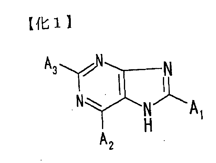 (A1, A2 and A3 independently show a hydrogen
atom, a hydroxyl base, and alkyl base or amino base
with carbons of 1 to 5, respectively)
(A1, A2 and A3 independently show a hydrogen
atom, a hydroxyl base, and alkyl base or amino base
with carbons of 1 to 5, respectively)
It is desirable that at least one of A2 and
A3 is hydroxyl in the above equation. In this case,
the compound has the structure which has amide
combination in the complex annulus, and the good anti-corrosion
operation and biodegradation.
A gas such as nitrogen, argon or helium and
can be used for the plasma process in the present
invention. For example, an ammonia plasma process can
be used as the plasma process under a deoxidizing
atmosphere. By carrying out the plasma process in the
deoxidizing atmosphere, the oxide on the wiring line
copper containing metal film surface can be deoxidized.
Also, when BTA is used as the anti-corrosion agent, it
is difficult for BTA to be removed, but BTA can be
removed through evaporation by carrying out the plasma
process immediately before the siliciding process.
The rinsing liquid in the present invention
can contain carboxylic acid or the salt. The
carboxylic acid may contain oxalic acid, citric acid,
malic acid, maleic acid, succinic acid, tartaric acid
or malonic acid.
Various type of low dielectric constant
materials can be used for an insulating film for a
wiring line and for an interlayer insulating film
between upper and lower wiring lines. Preferably, the
insulating film is a film containing ladder-type oxide
such as ladder-type siloxane hydride. For example,
the ladder-type siloxane hydride film, or a laminate
film of film of the ladder-type siloxane hydride film
and a SiO2 film is desirable. The ladder-type siloxane
hydride is a polymer which has a ladder-type molecule
structure. The dielectric constant is 2.9 or below
preferably from the viewpoint of the wiring line delay
prevention, and also the low film density is desirable.
For example, it is desirable that the film density is
from 1.50 g/cm3 to 1.58 g/cm3 and the refractive index
at the wavelength of 633 nm is from 1.38 to 1.40. As
a specific instance of such film material, L-Ox can be
exemplified.
Fig. 19 shows the structure of L-Ox (trade
mark) which has ladder-type siloxane hydride structure.
In Fig. 19, n is a positive number equal to or more
than 1. Fig. 29 shows the physical data of L-Ox with
such a structure.
It was confirmed from the observation result
of FT-IR that L-Ox has the structure of Fig. 19. It
was the sharp spectrum of a Si-H combination which
appeared in about 830 cm-1 that was characteristic in
the chart of Fig. 20. The steepness of this spectrum
suggests that L-Ox has a 2-dimension structure. Also,
the spectrum of another Si-H combination appeared near
870cm-1 in the higher wave number side with extremely
small peak. This fact would show that the measurement
object material has the 2-dimension structure.
The physical properties of L-Ox change
depending on the sintering condition. This fact will
be described with reference to Fig. 28.
When being sintered in a range of 200 C to
400 C in the atmosphere of inert gas such as nitrogen,
the L-Ox has following characteristic.
In Fig. 28, R.I. shows refractive index at
the wavelength of 633 nm. The refractive index is a
parameter which directly influences dielectric
constant, and this value changes between 1.38 to 1.40.
The value exceeds 1.40 when the sintering temperature
is less than 200 C or is higher than 400 C.
Also, the density of the L-Ox which is
sintered in the range of 200 C to 400 C is 1.50 to
1.58 g/cm3. The density exceeds 1.60 g/cm3 in case of
the sintering temperature over 400 C, and the density
could not be measured in case of the sintering
temperature less than 200 C.
Also, in the case of the sintering
temperature less than 200 C, a combination assumed to
be Si-OH was measured in about 3650 cm-1 from FTIR
spectrum. In the case of the sintering temperature
over 400 C, the increase of the density becomes
conspicuous.
From the above, it would be found that L-Ox
with a low dielectric constant characteristic can be
stably obtained through the sintering process in the
temperature range of 200 C to 400 C when an
insulating film containing the L-Ox is formed.
Fig. 21 shows the molecule skeleton of HSQ
(Hydrogen Silsesquioxane) with the hydrogen
Silsesquioxane structure and 3-dimentional structure
which are conventionally known (Semiconductor
Technology Outlook, 1998, pp. 431-435).
The materials of the two structures are
different from each other in the film stability in the
manufacture process and the L-Ox is conspicuously
excellent. This could be considered that the
decreasing amount of Si-H is less in the L-Ox,
compared with HSQ. Also, it could be considered as
one of the causes that that the state of the
combination of hydrogen atom in the insulating film is
different. That is, in HSQ, a hydrogen atom is
combined in the corner of the solid structure, whereas
in L-Ox a hydrogen atom is combined with the side of
the ladder structure. Therefore, it could be
considered that the density of the neighborhood of the
hydrogen atom is lower and the hydrogen combination in
HSQ becomes the structure which is wealthy in the
reactivity than L-Ox about HSQ. The difference in the
film stability between HSQ and L-Ox will be described
later with reference to the embodiments.
In the description below, it should be noted
that, the ladder-type siloxane hydride shown in Fig.
21 is appropriately described as L-Ox.
In the present invention, various films can
be used as the diffusion prevention film. However, it
is desirable that for example, sic, SiCN, SiOC, or
siON are used. By using the material of such a low
dielectric constant, the capacity between the wiring
lines can be reduced.
Also, when SiCN is used for the diffusion
prevention film, the advantage is achieved that the
manufacture reliability is improved when a siliciding
process of the wiring line is carried out. When
siliciding process is carried out, the formed silicide
layers are different between when SiCN is used for the
diffusion prevention film and when SiN is used. Figs.
27A and 27B shows examples of a sequence of gas and RF
power. In case of the SiN, the flowed gas is SiH4,
NH3, or N2. On the other hand, in case of the SiCN,
the flowed gas is trimethylsilane (hereinafter, are
3MS), SiH4, NH3, and N2. First, in the formation of a
SiN film, N2 is flowed without the application of RF
power, and the oxidation protection film (e.g., BTA)
in the wiring line surface is desorbed with heater
heat. Subsequently, SiH4 is introduced to form a
silicide layer on the Cu surface. Subsequently, NH3 is
introduced to form a SiN film. In this case, however,
in order to generate plasma stably before RF power is
applied, the mark is possible, it is necessary that
SiH4 and NH3 are introduced at the same time and the
gases are stabilized. At this time, SiH4 resolves on
the Cu wiring line surface and a silicide layer
becomes thicker excessively so that the deviation of
the wiring line layer resistance becomes large. On
the other hand, in case of the SiCN, N2 is first
flowed without the application of RF power, like SiN,
and the oxidation protection film (e.g., BTA) on the
wiring line surface is desorbed with the heater heat.
Subsequently, SiH4 is introduced and a silicide layer
is formed on the Cu surface. Next, the SiH4 gas is
stopped and 3MS and NH3 gas are introduced and then
the step of the gas stabilization is started. In this
case, because 3MS is not resolved on the Cu surface,
the unnecessary silicide layer is not formed unlike
the case of the SiN and it is possible to suppress the
deviation of the wiring line layer resistance.
Next, the semiconductor device with a copper
containing wiring line structure according to the
first embodiment of the present invention will be
described.
Fig. 2 is a cross sectional view showing an
example of the semiconductor device according to the
present invention. A MOS transistor is formed to have
a gate electrode 102, diffusion layers 104 on a
silicon substrate 100. An insulating film 106 is
formed to cover the MOS transistor. The copper
connection plug s108 are formed in the insulating film
106 to connect with the diffusion layers 104 and a
first copper wiring line 22a, a connection plug 28 and
a second copper wiring line 22b are formed in order on
the surface portion. A copper wiring line layer is
formed to have the same or similar structure on the
surface portion of the layer containing the copper
wiring line, and a passivation film 114 is provided
for the uppermost layer. It should be noted that the
first copper wiring line 22a is electrically connected
with the device formed on the silicon substrate 100.
Also, a set of the first copper wiring line 22a, the
connection plug 28 and the second copper wiring line
22b to be described below may be provided for
whichever layer of the semiconductor device shown in
Fig. 2.
The embodiments of the present invention will
be described with reference to a wiring line structure
surrounded by the dotted line section 116 of Fig. 2 as
an example.
Fig. 3 is a cross sectional view showing the
wiring line structure in the first embodiment of the
present invention. A first laminate layer 14a in
which a first SiCN film 12, L-Ox film and a SiO2 film
are laminated in this order, and a second laminate
layer 14b in which a second SiCN film 16, a silicon
oxide film 18, a third SiCN film 20 and a L-Ox film
and a SiO2 film are laminated are laminated on an
insulating film 106 on the silicon substrate (not
shown). In the first laminate layer 14a and the
second laminate layer 14b, the first copper wiring
line 22a and the second copper wiring line 22b are
formed, respectively.
The first copper wiring line 22a are formed
of a tantalum-based barrier metal film 24a and a
copper film 26a. In the silicon oxide film 18, a
connection plug 28 is formed to connect with the
surface of the first copper wiring line 22a. The
connection plug 28 is formed of a tantalum-based
barrier metal film 30 and a copper film 32. In the
second laminate layer 14b, the second copper wiring
line 22b is formed to connect with the surface of the
connection hole. The second copper wiring line 22b is
formed of a tantalum-based barrier metal film 24b and
the copper film 26b. Also, a first Cu silicide layer
34a is formed on the surface of the first copper
wiring line 22a, and the second Cu silicide layer 34b
is formed on the surface of the second copper wiring
line 22b, respectively.
Hereinafter, the manufacturing method of the
wiring line structure 1 of the first embodiment shown
in Fig. 3 will be described with reference to Figs. 4A
to 4N.
Fig. 4A shows the structure in which a wiring
line groove is formed in first SiCN film 12 and the
first laminate layer 14a. This structure is formed by
etching the first SiCN film 12 and the first laminate
layer 14a step-by-step after the first SiCN film 12
and the first laminate layer 14a are formed and then a
resist film (not shown) is patterned into a
predetermined shape.
Next, the tantalum-based barrier metal film
24a is formed in which Ta and TaN are deposited on the
substrate surface (the film thickness of about 20 nm
for Ta, and the film thickness of about 10 nm for TaN)
by a sputtering method and a reactivity sputtering
method (Fig. 4B).
Subsequently, as shown in Fig. 4C, the copper
film 26a is formed on the tantalum-based barrier metal
film 24a. The copper film 26a is formed as follows by
a plating method. First, a seed copper film of copper
is deposited by the sputtering method for growth of a
copper plating film. Next, the substrate is immersed
in copper sulfate solution with the liquid temperature
of about 25 C so that the copper film 26a is formed
by an electrolysis plating method (the film thickness
of about 600 nm in a flat section).
Next, an annealing process is carried out to
the substrate thus obtained, for about 30 minutes at
350 C. Through the annealing process at such a high
temperature, the particle diameter of a grain in the
copper film 26a becomes large, compared with the
particle diameter before the annealing process.
Thus, a portion where a plurality of boundaries of the
grains exposed in the surface of the copper film 26a
overlap decreases relatively. Therefore, it becomes
difficult for the cavity to be produced. Also, the
resistance value of the first copper wiring line 22a
after such an annealing process decreases the
resistance value thereof before the annealing process.
For example, the annealing process may be carried out
in a temperature range of 200 C to 500 C.
Next, the unnecessary copper film 26a and the
tantalum-based barrier metal film 24a which are formed
outside the wiring line groove are removed by a
chemical mechanical polish (CMP) method. The copper
film 26a and so on are left inside the wiring line
groove. Thus, the first copper wiring line 22a is
formed (Fig. 4D).
The anti-corrosion process is carried out in
which the surface of the copper film 26a is processed
by BTA as an anti-corrosion agent immediately after
the CMP process to the copper film 26a. Here, 0.05%
BTA solution is used. By this, the surface of the
copper film 26a is protected by BTA when a sample is
transferred for the following process after the CMP
process. Therefore, the copper film 26a can be
prevented from being oxidized.
Next, as shown in Fig. 4E, the first Cu
silicide layer 34a is formed on the surface of the
copper film 26a of the first copper wiring line 22a.
The method of forming the first Cu silicide layer 34a
will be described below.
After BTA is removed through evaporation by
an ammonia plasma process (for 30 seconds at 350 C),
SiH4 is flowed for about 60 seconds (the flow rate of
SiH4 is 5000 sccm, while the flow rate of N2 is 50
sccm) under the pressure of 3 torr at the temperature
of 350 C. Thus, the surface of the copper film 26a
is silicided. The first Cu silicide layer 34a with
the thickness of about 10 nm is formed. By the
fluorescence X ray analysis, the existence of CuSix is
confirmed.
Next, the second SiCN film 16 (the film
thickness of about 70 nm), the silicon oxide film 18
(the film thickness of about 350 nm) are formed (Fig.
4F).
Next, the silicon oxide film 18 is etched
using a lithography method until the second SiCN film
16 is exposed. Subsequently, the etching gas is
replaced and the second SiCN film 16 is etched until
the surface of the first Cu silicide layer 34a is
exposed. Thus, as shown in Fig. 4G, the connection
hole 40 is formed.
Next, in order to fill the inside of the
connection hole 40, the tantalum-based barrier metal
film 30 and the copper film 32 (the thickness of about
650 nm in the flat section) are formed in this order
(Fig. 4H). The copper film 32 is formed by the
plating method like the copper film 26a of the first
copper wiring line 22a. Subsequently, a flattening
process by the CMP is carried out and the connection
plug 28 is formed (Fig. 4I).
Next, the third SiCN film 20 (the film
thickness of about 70 nm) and the second laminate
layer 14b (the film thickness of about 300 nm) are
formed on a surface portion of the connection plug 28
(Fig. 4J). Then, the wiring line groove 42 is formed
by a dry etching (Fig. 4K). Subsequently, the
tantalum-based barrier metal film 24b and the copper
film 26b are formed in this order (the film thickness
of about 600 nm in the flat section) in order to fill
the groove 42 (Fig. 4L). The copper film 26b is
formed with the plating method like the copper film
26a of the first copper wiring line 22a. Subsequently,
the flattening process by the CMP process is carried
out and the second copper wiring line 22b is formed
(Fig. 4M). Subsequently, the anti-corrosion process
to the copper film 26b by BTA is carried out. After
BTA is removed in the evaporation by the ammonia
plasma process, a siliciding process is carried out
and the second Cu silicide layer 34b is formed (Fig.
4N).
As mentioned above, the wiring line structure
is formed as shown in Fig. 3. By repeating the above-mentioned
processes, it is possible to manufacture the
semiconductor device with the multiple wiring line
structure of 3 or more layers, as shown in Fig. 2.
The second embodiment is different from the
first embodiment in that BTA is evaporated and removed
through a heating process at about 350 C instead of
the ammonia plasma process, before the siliciding
process of the surface of the copper film 26a and the
surface of the copper film 26b. Through the heating
process, the wiring line structure shown in Fig. 3 is
formed. It should be noted that the heating
temperature at which BTA is evaporated and removed may
be from 150 C to 450 C. By the fluorescence X ray
analysis of the formed wiring line structure, the
existence of CuSix is confirmed.
By carrying out the ammonia plasma process
for the evaporation and removal of the BTA as in the
first embodiment, the siliciding process can be
carried out while BTA is removed. Therefore, it is
possible to control the siliciding process such as a
film thickness control of the Cu silicide. Also, by
carrying out the heating process for the evaporation
and removal of the BTA as in the second embodiment,
the corrosion of the boundaries of the grains in the
surface of the copper film 26a or the surface of the
copper film 26b by gas such as ammonia can be
prevented. Therefore, the good wiring line structure
can be formed.
Fig. 5 is a diagram showing the wiring line
structure in the third embodiment. The third
embodiment is different from the first embodiment in
that the first Cu silicide layer 34a and the second Cu
silicide layer 34b are not formed, and that the BTA
anti-corrosion processing is not carried out. The
description of the same components of Fig. 5 as those
of Fig. 3 will be omitted by allocating the same
reference numerals.
In the third embodiment, the processes are
carried out as in the first embodiment until the CMP
process to the copper film 26a of the first copper
wiring line 22a process. Subsequently, the second
SiCN film 16 and the silicon oxide film 18 are formed
without carrying out the siliciding process of the
surface of the copper film 26a. Before the second
SiCN film 16 is formed, a surface treat process of the
copper film 26a of the first copper wiring line 22a is
carried out by the ammonia plasma process. The
process after the silicon oxide film 18 is formed is
also the same as the first embodiment. The wiring
line structure shown in Fig. 5 is formed through the
above processes.
The fourth embodiment is different from the
third embodiment in that BTA anti-corrosion processing
is carried out immediately after the CMP process to
the surface of the copper film 26a or the surface of
the copper film 26. Subsequently, before forming of
second SiCN film 16, a surface treating of the copper
film 26a of the first copper wiring line 22a is
carried out by the ammonia plasma process. The wiring
line structure similar to that shown in Fig. 5 is
formed through this process. In this way, the
surfaces of the copper films 26a and 26b can be
protected by the BTA anti-corrosion process
immediately after the CMP process. Therefore, the
'reliability of the semiconductor device containing
such a copper wiring line can be increased through the
anti-corrosion operation to on the copper film
surfaces.
Figs. 6A to 6F are cross sectional views
showing the wiring line structure manufacturing
process in the fifth embodiment. The fifth embodiment
is different from the first embodiment in that the
connection plug 28 and the second copper wiring line
22b are formed by the dual damascene method. The same
components of Figs. 6A to 6F as those of Fig. 3 are
allocated the same reference numerals, and the
description will be omitted.
First, the first copper wiring line 22a is
formed as in the first embodiment described with
reference to Figs. 4A to 4N. Then, the first Cu
silicide layer 34a is formed on the surface of the
copper film 26a (Fig. 6A).
Next, the second SiCN film 16 and the silicon
oxide film 50 are formed (Fig. 6B).
Next, as shown in Fig. 6C, a connection hole
52 for the connection plug 28 and a wiring line groove
54 are formed in the silicon oxide film 50 by a step-by-step
etching method using a lithography method.
Subsequently, the etching gas is changed and the
etching of the second SiCN film 16 is carried out.
Subsequently, as shown in Fig. 6D, the tantalum-based
barrier metal film 56 is formed on the whole surface
of the silicon oxide film 50 containing the connection
hole 52 and the wiring line groove 54. The tantalum-based
barrier metal film 56 is formed of a Ta film and
a TaN film.
Next, as shown in Fig. 6E, a copper film 58
is formed on the tantalum-based barrier metal film 56
to fill the connection hole 52 and the wiring line
groove 54. Subsequently, a CMP flattening process is
carried out to remove the copper film 58 and the
tantalum-based barrier metal film 56 from a portion
other than the wiring line groove 54. Through this
process, the connection plug 28 and the second copper
wiring line 22b are formed. Subsequently, the BTA
anti-corrosion process is carried out. After the BTA
is evaporated and removed by the ammonia plasma
process, a siliciding process is carried out. Thus,
the second Cu silicide layer 34b is formed (Fig. 6F).
The wiring line structure in the fifth embodiment is
formed by above processes. The existence of CuSix was
confirmed by the fluorescence X ray analysis of the
formed wiring line structure. Also, the existence of
an amorphous region was confirmed in the wiring line
structure formed in the first, second and fifth
embodiments by the X ray diffraction.
2-layer wiring line structures as shown in
Fig. 7A are formed by the methods in the first to
fifth embodiments to examine the production yields,
respectively. The 2-layer wiring line structure is
called a via-chain. The 10,000 first copper wiring
lines 22a are provided in parallel and the 10,000
second copper wiring lines 22b are provided in
parallel to be orthogonal to the first copper wiring
lines. These wiring lines are connected by 20,000
connection plugs 28. In the figure, the semiconductor
substrate, an interlayer insulating film and so on are
omitted. When a predetermined voltage is applied
between the two ends of this via-chain, the current
flows in the direction shown in Fig. 7B by the arrows.
Thus, the resistance of the 10,000 first copper wiring
lines 22a, the 10,000 second copper wiring lines 22b
and the 20,000 connection plugs 28 is measured. The
2-layer wiring line structures corresponding to the
first to fifth embodiments are called the wiring line
structures 1 to 5, respectively. The existence of
CuSix was confirmed in the wiring line structures 1, 2
and 5 by the fluorescence X ray analysis.
Also, a comparison sample is formed in which
the copper film 26a of the first copper wiring line
22a is formed, and the BTA anti-corrosion process and
the ammonia plasma process are carried out, and then
the connection plug 28 and the second copper wiring
line 22b are formed by the dual damascene method
without the siliciding process of the surface of the
copper film 26a (Wiring line structure 6).
After being formed, the wiring line structure
from 1 to 6 were located for 500 hours at the
temperature of 150 C. Subsequently, the production
yield examination of the via-chains was carried out.
Also, a sample as a reference was prepared in which
SiH4 gas was flowed to form a silicide layer while
generating plasma (Wiring line structure 7). The
production yield of the via-chain was measured in the
2-layer wiring line structures (reference wiring line
structure 1 and reference wiring line structure 2)
which were formed like the wiring line structures 1
and the wiring line structure 5 and were left for 500
hours at the room temperature. The following table 1
shows the production yield (%) of each wiring line
structure when it was supposed that the production
yields in the reference wiring line structures 1 and 2
were 100% and the production yield in the wiring line
structure 6 was 0%.
| Product yield(%) | ||
| WS1 (150 C, 500hr) | BTA-NH3pl-SiH4-single | 98 |
| WS2 (150 C, 500hr) | BTA-SiH4- | 100 |
| WS3 (150 C, 500hr) | NH3pl-Single | 15 |
| WS4 (150 C, 500hr) | BTA-NH3pl-single | 40 |
| WS5 (150 C, 500hr) | BTA-NH3pl-SiH4-double | 90 |
| WS6 (150 C, 500hr) | BTA-NH3pl-double | 0 |
| RWS1 (150 C, 500hr) | BTA-NH3pl-SiH4-single | 100 |
| RWS2 (150 C, 500hr) | BTA-NH3pl-SiH4-double | 100 |
| WS: wiring line structure | ||
| RWS: reference wiring line structure | ||
| NH3pl: NH3 plasma |
Fig. 8 is a graph showing data of the
production yield shown in table 1. As shown in Fig. 8,
there is no difference between the single damascene
method and the dual damascene method in the reference
wiring line structures 1 and 2 which were left at the
room temperature is not present. Also, the production
yield is approximately 100% in the wiring line
structure 1 and the wiring line structure 2 in which
the BTA anti-corrosion process and the siliciding
process are carried out and which are formed using the
single damascene method.
The production yield is 40% in the wiring
line structure 4 which is formed using the single
damascene method like the wiring line structure 1 and
the siliciding process is not carried out. This value
is less than a half of the production yield of the
wiring line structure 1. It could be considered that
this results from that the copper film 26a of the
first copper wiring line 22a is protected by the first
Cu silicide layer 34a, and a stress from the second
copper wiring line 22b as an upper layer and
connection plug 28 is relaxed so that the generation
of the cavity in the first copper wiring line 22a can
be prevented.
The production yield is 90% in the wiring
line structure 5 which is formed by the dual damascene
method and in which the siliciding process is carried
out. This production yield is greatly improved,
compared with the wiring line structure 6 (production
yield of 0%) in which the siliciding process is not
carried out although it is formed using the dual
damascene method. It could be considered that the
increase of the production yield results from that the
copper film 26a of the first copper wiring line 22a is
protected by the first Cu silicide layer 34a, and a
stress from the second copper wiring line 22b as an
upper layer and connection plug 28 is relaxed so that
the generation of the cavity in the first copper
wiring line 22a can be prevented.
Also, the production yield is improved in the
wiring line structure 1 formed using the single
damascene method, compared with the wiring line
structure 5 formed using the dual damascene method.
In the wiring line structure 5, the sucking-up of
copper into the connection plug 28 occurs from the
second copper wiring line 22b formed using the dual
damascene method. As a result, a cavity is produced
between the connection plug 28 and the first copper
wiring line 22. However, in the wiring line structure
1 formed using the single damascene method, the
generation of such a cavity could be prevented.
Also, the production yield is 15% in the
wiring line structure 3 in which neither of the BTA
anti-corrosion process and the siliciding process are
carried out. This value is improved, compared with
the production yield in the wiring line structure 6 in
which the BTA anti-corrosion process is carried out
and is formed using the dual damascene method. From
the above, it could be understood that the formation
of the copper wiring line by the single damascene
method results in the improvement of the production
yield.
Moreover, as for the wiring line structures
in which the siliciding process is not carried out,
the production yield is decreased by the difference in
the production yield between the wiring line structure
5 and the wiring line structure 1 or more, in the
wiring line structure 6 formed using the dual
damascene method, compared with the wiring line
structure 4 formed using the single damascene method.
It could be considered that this results from that the
sucking-up of copper by the second copper wiring line
22b happens from the first copper wiring line 22a in
addition to the connection plug 28, so that the cavity
is generated between the first copper wiring line 22a
and the connection plug 28 when the surface of the
copper film 26a of the first copper wiring line 22a is
not protected by the first Cu silicide layer 34a.
Also, a leak current is measured between the
wiring lines in each wiring line structure. The
result is shown in Figs. 26A and 26B. The leak
current is hardly present in the wiring line
structures 1 to 6. However, the leak current is large
in the wiring line structure 7 in which plasma is
generated and the silicide layer is formed. This
could be considered as the result that a polysilicon
layer is formed on the wiring line insulating film and
Cu atoms are diffused into the insulating film.
From the above results, it is found that the
production yield can be increasingly improved by
protecting the copper film 26a of the first copper
wiring line 22a by the first Cu silicide layer 34a.
Also, it is found that the production yield is greatly
improved even if the second copper wiring line 22b is
formed on the connection plug 28 provided on the first
copper wiring line 22a and the surface peripheral
portion of the connection plug 28 using the single
damascene method. Also, it is found that the
production yield further improved by the combination
of the protection of the copper film 26a by the first
Cu silicide layer 34a and the formation of the
connection plug 28 and the second copper wiring line
22b using the single damascene method. Also, it is
found that it is preferable from the prevention of
leak between wiring lines that the silicide layer is
formed without generating plasma.
It should be noted that the production yield
examination of the via-chain was carried out in the
same way to the wiring line structure which was formed
in the similar processes to the first, second and
fifth embodiments and a process was added that the
surface of the copper film 26a is rinsed with oxalic
acid before the BTA anti-corrosion process after the
CMP process to the copper film 26a of the first copper
wiring line 22a. The result was equal to or better
than the above-mentioned result. It could be
considered that this results from that the chelate
operation of the oxalic acid effectively removes a
copper oxide (CuOx) film from the surface of the
copper film 26a.
The seventh embodiment is different from the
first embodiment or the second embodiment in a method
of forming the first copper wiring line 22a and the
second copper wiring line 22b. As described with
reference to Figs. 4A to 4N in the first embodiment,
the tantalum-based barrier metal film 24a is formed in
the wiring line groove.
Hereinafter, the manufacturing method of the
first copper wiring line 22a in the seventh embodiment
will be described with reference to Figs. 13A to 13D.
First, a seed copper film 60 (about 100 nm) is formed
by a sputtering method on the tantalum-based barrier
metal film 24a. Subsequently, in order to fill a part
of the wiring line groove, a plating copper film 62
(the film thickness of about 150 nm in the flat
section) is formed on the seed copper film 60 by the
electrolysis plating method (Fig. 13A). At this time,
the plating copper film 62 has (111) orientation.
Also, it is assumed that the total film thickness of
the seed copper film 60 and the plating copper film 62
is t1.
Subsequently, the copper oxide in the surface
of the plating copper film 62 is sputtered and
deoxidized by the Ar/H2 plasma with the room
temperature in a cleaning chamber. A bias sputtering
copper film 64 (the film thickness of about 900 nm in
a flat section) is formed on the plating copper film
62 in the Cu sputtering chamber by a bias sputtering
method without exposing the substrate to the
atmosphere by applying a DC bias to the silicon
substrate (Fig. 13B). The bias sputtering copper film
64 is formed while argon ions are irradiated to a
sputtering growth surface. At this time, the ion
irradiation energy applied to the silicon substrate
(the plasma potential + self bias) is a high bias,
e.g., 80 eV or more, preferably, 200 eV or more. In
order to prevent the temperature rise by the plasma
irradiation during the growth of the film, the
substrate temperature is set to -5 C. Also, the bias
sputtering copper film 64 is formed to have the film
thickness t2 of the bias sputtering copper film 64
thicker than the above-mentioned t1. At this time, it
is confirmed that the bias sputtering copper film 64
had (111) orientation.
Next, a heat treatment process is carried out
for 30 minutes at 400 C in the inert gas atmosphere.
Through the heat treatment process, the crystal
orientation of the bias sputtering copper film 64,
plating copper film 62 and seed copper film 60 changes
to (200). At the same time, a copper film 66 is
formed to have the average grain size of the huge
grains of hundreds of µm (Fig. 13C). Fig. 17 is a
diagram showing the analysis result of the copper film
66 formed as mentioned above by the X-ray diffraction
method. As shown in this figure, the grains of 93%
(190468/204419) or more have plane orientation (200)
in the copper film 66 surface. Also, when the grain
size in the surface of the copper film 66 is confirmed
by the optical microscope, most of the grains are
larger than 100 to 200 µm, or more and some are larger
than 500 µm.
Next, the unnecessary copper film 66 and the
tantalum-based barrier metal film 24a formed outside
the wiring line groove are removed by the CMP process
such that only the copper film 66 and so on are left
inside the wiring line groove. Thus, the first copper
wiring line 22a is formed (Fig. 13D). A part of the
samples is examined in this step. It could be
confirmed that a 70% of the copper film 66 of the
first copper wiring line 22a is formed with single
grains. In this case, the wiring line width of the
first copper wiring line 22a is 10 µm, the length of
the wiring line is 100 µm and the film thickness is
300 nm.
After this, the surface process of the copper
film 66 by BTA is carried out like the second
embodiment, and the first Cu silicide layer 34a is
formed after the BTA is evaporated and removed by the
heating process of about 350 C. Subsequently, the
connection plug 28 is formed like the first embodiment
and the second embodiment. The second copper wiring
line 22b is formed like the first copper wiring line
22a mentioned above in this embodiment.
As mentioned above, a bias sputtering copper
film 64 is formed on the plating copper film 62, and
then a heat-treating is carried out. Thus, the plane
orientation of the crystal of copper can be controlled.
In this way, the surface of copper film 66 can be
uniformly kept, and the Cu silicide layer can be
uniformly formed on the copper film 66. Therefore,
the film thickness of the Cu silicide layer can be
appropriately controlled, and while suppressing the
resistance increase rate of the first copper wiring
line 22a and the second copper wiring line 22b, these
wiring lines can be protected.
Moreover, because the grain size of copper
can be made large through the above mentioned heat
treatment process, the number of the boundaries of the
grains in the copper film 66 surface can be
substantially reduced. Thus, the stress migration
endurance of the wiring line structure can be
increased. Also, in the seventh embodiment, the Cu
silicide layer is formed in the surface of the copper
film 66. Therefore, the displacement of the crystal
of copper can be suppressed, and the stress migration
endurance of the wiring line structure can be improved.
Also, because the grain size of the copper film of the
copper wiring line can be made large, the wiring line
resistance can be reduced. Also, because the boundary
of the grain is hardly generated in the surface of the
copper film 66 in this embodiment, the Cu silicide can
be uniformly formed from this viewpoint. It could be
confirmed by an outward appearance test apparatus
(KLA-Tencor) that the Cu silicide layer is formed
uniformly in the wiring line surface in this
embodiment.
The eighth embodiment is different from the
seventh embodiment in that a CVD copper film 68 is
formed by a plasma CVD method instead of that the seed
copper film 60 and plating copper film 62 when the
first copper wiring line 22a and the second copper
wiring line 22b are formed.
The eighth embodiment will be described with
reference to Figs. 14A to 14D. After the tantalum-based
barrier metal film 24a is formed, the CVD copper
film 68 is formed by the plasma CVD method (the film
thickness of about 200 nm in a flat section) (Fig.
14A). At this time, the crystal orientation of the
CVD copper film 68 is (111).
Next, the copper oxide in the CVD copper film
68 surface is sputtered and reduced by the Ar/H2
plasma with the room temperature in the cleaning
chamber like the seventh embodiment. Without exposing
the substrate to the atmosphere, a DC bias is applied
to the substrate in the Cu sputtering chamber, and a
bias sputtering copper film 64 is formed on the CVD
copper film 68 by the bias sputtering method (the film
thickness of about 900 nm in a flat section) (Fig.
14B). The condition of the bias sputtering is like
the seventh embodiment. Also, in this embodiment, the
bias sputtering copper film 64 is formed such that the
film thickness t4 of bias sputtering copper film 64 is
thicker than the film thickness t3 of the CVD copper
film 68, like the seventh embodiment.
Next, a heat treatment process is carried out
for 30 minutes at 400 C in the inert gas atmosphere.
Through the heat treatment process, the crystal
orientation of the bias sputtering copper film 64 and
the CVD copper film 68 is changed to (200), and at the
same time, the copper film 66 is formed to have the
huge grains with the average grain size of hundreds of
µm (Fig. 14C).
Next, the unnecessary copper film 66 and the
tantalum-based barrier metal film 24a formed outside
the wiring line groove are removed by the CMP process.
The first copper wiring line 22a is formed such that
only the copper film 66 and so on are left inside the
wiring line groove (Fig. 14D).
After this, the first Cu silicide layer 34a
and the connection plug 28 are formed like the seventh
embodiment. The second copper wiring line 22b is
formed like the above-mentioned first copper wiring
line 22a in this embodiment.
The ninth embodiment is different from the
seventh embodiment in the method of forming the
connection plug 28. After the first copper wiring
line 22a is formed, as described in the seventh
embodiment, the connection hole 40 is formed in the
second SiCN film 16 and the silicon oxide film 18, as
described with reference to Fig. 4A to 4L in the first
embodiment. Subsequently, the tantalum-based barrier
metal film 30 is formed inside the connection hole 40
(Fig. 15A).
Next, the seed copper film 70 is formed on
the tantalum-based barrier metal film 30 by the
sputtering method. Subsequently, the plating copper
film 72 is formed on the seed copper film 70 by the
electrolysis plating method (Fig. 15B). Subsequently,
a DC bias is applied to the substrate and a bias
sputtering copper film 74 is formed on the plating
copper film 72 by the bias sputtering method (Fig.
15C). In this case, the bias sputtering copper film
74 is formed while argon ions are irradiated to the
sputtering growth surface. The condition of the bias
sputtering is like the seventh embodiment. Also, the
bias sputtering copper film 74 is formed such that the
film thickness t6 of the bias sputtering copper film
74 is larger than the total film thickness t5 of the
seed copper film 70 and the plating copper film 72.
Next, the heat treatment process is carried
out in the inert gas atmosphere. Through this heat
treatment process, the crystal orientation of the bias
sputtering copper film 74, the plating copper film 72
and the seed copper film 70 changes to (200). At the
same time, the copper film 76 is formed to have the
huge grains with the average grain size of hundreds of
µm (Fig. 15D).
Next, a CMP flattening process is carried out
as described with reference to Figs. 4A to 4N in the
first embodiment and the connection plug 28 is formed.
Subsequently, the second copper wiring line 22b is
formed like the seventh embodiment.
In the ninth embodiment, the plane
orientation of the crystal in the surface of the
copper film of he connection plug 28 can be made (200).
The grain size of copper can be made large. Therefore,
the stress migration endurance of the connection plug
28 can be increased. Also, because the grain size of
the copper film of a copper wiring line and a plug can
be made large, the wiring line resistance can be
reduced.
The tenth embodiment is different from the
fifth embodiment in the method of forming the first
copper wiring line 22a and the second copper wiring
line 22b. The connection hole 52 and the wiring line
groove 54 are formed as described with reference to
Figs. 6A to 6F in the fifth embodiment. The tantalum-based
barrier metal film 56 is formed on the whole
surface of the silicon oxide film 50 containing the
connection hole 52 and the wiring line groove 54. It
should be noted that in the tenth embodiment, the
first copper wiring line 22a is formed in the same
method as the second copper wiring line 22b to be
described below.
Hereinafter, the manufacturing method of the
second copper wiring line 22b in the tenth embodiment
will be described with reference to Figs. 16A to 16D.
First, the seed copper film 80 (about 100 nm) is
formed on tantalum-based barrier metal film 56 by the
sputtering method (Fig. 16A). Next, the plating
copper film 82 is formed on seed copper film 80 by the
electrolysis plating method (the film thickness of
about 200 nm in a flat section) (Fig. 16B). At this
time, the plating copper film 82 has (111) orientation.
It is assumed that the total film thickness of the
seed copper film 80 and the plating copper film 82 is
t7.
The copper oxide in the plating copper film
82 surface is sputtered and deoxidized by the Ar/H2
plasma with the room temperature in the laundering
chamber. Without exposing the substrate to the
atmosphere, a DC bias is applied to the substrate in
the Cu sputtering chamber, and the bias sputtering
copper film 84 is formed on the plating copper film 82
by the bias sputtering method (the film thickness of
about 900 nm in a flat section) (Fig. 16C). The bias
sputtering copper film 84 is formed while argon ions
are irradiated to the sputtering growth surface. In
this case, the ion irradiation energy applied to the
silicon substrate (the plasma potential + self bias)
is a high bias, e.g., 80 eV or more, preferably, 200
eV or more. The substrate temperature is set to -5 C
to prevent temperature rise by the plasma irradiation.
Also, the bias sputtering copper film 84 is formed
such that the film thickness t8 of the bias sputtering
copper film 84 is thicker than the above-mentioned t7.
Next, the heat treatment process is carried
out for 30 minutes at 400 C in the inert gas
atmosphere. Through the heat treatment process, the
crystal orientation of the bias sputtering copper film
84, the plating copper film 82 and the seed copper
film 80 changes to (200). at the same time, the
copper film 86 is formed to have the huge grain with
the average grain size of hundreds of µm (Fig. 16D).
Next, the CMP flattening process is carried
out, as described with reference to Figs. 6A to 6F in
the fifth embodiment and the second copper wiring line
22b is formed.
Next, the surface treat process of the copper
film 86 by BTA is carried out like the fifth
embodiment. Subsequently, the second Cu silicide
layer 34b is formed after the BTA is evaporated and
removed by the heating process of about 350 C.
The plane orientation of the copper crystal
can be controlled by forming the bias sputtering
copper film 84 on the above-mentioned plating copper
film 82 and carrying out the heat treatment process.
In this way, the surface of the copper film 86 can be
uniformly kept. Therefore, the Cu silicide layer can
be uniformly formed on the copper film 86. Also, the
film thickness of the Cu silicide layer can be
appropriately controlled, and while suppressing the
resistance increase rate of the first copper wiring
line 22a and the second copper wiring line 22b, these
wiring lines can be protected.
Moreover, the grain size of copper can be
made large through the above-mentioned heat treatment
process. Therefore, the number of boundaries of the
grains in the copper film 86 surface can be
substantially reduced. Thus, the stress migration
endurance of the wiring line structure can be
increased. Also, because the Cu silicide layer is
formed in the copper film 86 surface in the tenth
embodiment, the displacement of the crystal of copper
can be suppressed. Moreover, the stress migration
endurance of the wiring line structure can be improved.
Also, because the grain size of the copper film of the
copper wiring line and the plug can be made large, the
wiring line resistance can be reduced. Also, because
the grain size of the copper film of the copper wiring
line can be made large, the wiring line resistance can
be reduced. Moreover, because the boundary of the
grain is hardly generated in the copper film 86
surface at this embodiment, the Cu silicide layer can
be uniformly formed from this viewpoint.
The 2-layer wiring line structures as shown
in Fig. 7A are formed in the method mentioned in the
above second, fourth and seventh embodiments and the
production yield of the via-chain resistance is
measured like the sixth embodiment. Here, the
1,000,000 first copper wiring lines 22a are provided
in parallel and the 1,000,000 second copper wiring
lines 22b are provided in parallel so as to be
orthogonal to the wiring lines 22a. 2,000,000
connection plugs 28 are connected between these wiring
lines. The 2-layer wiring line structure
corresponding to the second, fourth and seventh
embodiments are respectively called wiring line
structure a2, wiring line structure a4 and wiring line
structure a7. It was confirmed by the fluorescence X
ray analysis that the CuSix is present in the wiring
line structure a2 and the wiring line structure a7.
The wiring line structure a2, the wiring line
structure a4 and the wiring line structure a7 were
left for 500 hours at the temperature 150 C. With
each of the wiring line structures, the initial value
of the resistance value of the via-chain is set to
100% and the resistance value of the sample is
calculated as a relative value. The table shows a
range of resistance values when a plurality of samples
are prepared and the evaluation is carried out. The
higher value shows the higher stress migration
endurance.
| Method | Cu silicide | Product yield (%) | |
| WS a2 | plating | present | 60-78 |
| WS a4 | plating | no | 8-24 |
| WS a7 | Plating-bias sputtering | present | 93-100 |
| WS: wiring line structure |
As shown in the table 2, the copper films
formed in the plating method and the bias sputtering
method are subjected to the heat treat process. The
plane orientation of the crystal in the surface of the
copper film is changed to (200) and the grain is grown
largely. Then, the production yield is 93 to 100% in
the wiring line structure a7 in which the siliciding
process is carried out. The production yield is
better than the production yield of 60 to 78% in the
wiring line structure a2 in which the siliciding
process is carried after a copper film is formed by
the plating method. Also, the production yields in
the wiring line structure a7 and the wiring line
structure a2 are greatly improved more than that of
the wiring line structure a4 in which the copper film
is formed by the plating method but the siliciding
process is not carried out. In this way, from the
result of the eleventh embodiment, it could be
confirmed that it is possible to effectively restrain
the stress migration by siliciding the surface of the
wiring line formed of copper. Moreover, it could be
confirmed that the stress migration could be further
restrained by making a plane orientation in the
surface of the copper film uniform and making the
grains of the copper film large to reduce the number
of grains in the copper film surface.
The twelve embodiment is different from the
seventh to tenth embodiments in that a tungsten cap
layer is a formed instead that the Cu silicide layer
34a or 34b is formed on the surface of the first
copper wiring line 22a and the second copper wiring
line 22b shown in Fig. 2.
After the copper film 66 is formed like the
seventh embodiment, an unnecessary copper film 66 and
tantalum-based barrier metal film 24a formed outside
the wiring line groove are removed by the CMP process.
The copper film 66 and so on are left inside only the
wiring line groove. Thus, the first copper wiring
line 22a is formed. Subsequently, WF6 and H2 are made
to act for about 60 seconds in a W-CVD chamber and a
tungsten cap layer is formed on the copper film 66
surface of the first copper wiring line 22a.
Next, a silicon oxide film 18 is formed
directly on the first copper wiring line 22a without
the second SiCN film 16 being formed. Subsequently,
the connection plug 28 is formed like the seventh
embodiment and the second copper wiring line 22b is
formed as in the above-mentioned first copper wiring
line 22a.
The copper film on the copper wiring line
surface is protected by the tungsten cap layer in the
wiring line structure thus obtained. Therefore, it is
possible to prevent the oxidation of the copper film
surface and the diffusion of copper into the
interlayer insulating film, even if the diffusion
prevention film such as the second SiCN film 16 shown
in Fig. 2 is not formed or the diffusion prevention
film is thin. In this way, the capacity of the
semiconductor device can be reduced and the
semiconductor device can be manufactured to meet the
demand of the high speed operation. Also, cross talk
between the wiring lines can be reduced.
Also, in the wiring line structure formed in
the twelfth embodiment, the tungsten cap layer is
formed on the surface of the copper film 66 in which
the grain size is large and the plane orientation is
uniform. Therefore, the film thickness can be made
uniform, compared with the film formed on the copper
film surface formed by only the usual plating method,
and the wiring line resistance can be reduced.
It should be noted that various processes
described in each embodiment may be appropriately
combined.
Two kinds of wiring line structures are
formed using L-Ox and HSQ, and the siliciding process
is carried out through the SiH4 irradiation. In this
case, it could be confirmed that the endurance of the
film was largely changed. Hereinafter, the experiment
data will be described.
The SiH4 irradiation is carried out in a
chamber of the plasma CVD apparatus and the condition
is the process temperature of 350 C, the process
pressure of about 4 Torr, the SiH4 flow rate of 50
sccm, and the N2 flow rate of 2500 sccm. HSQ and L-Ox
are coated and baked at about 200 C by a hot plate
and then sintered for 30 minutes in the nitrogen
atmosphere of 350 C in a diffusion furnace. Thus,
blank wafers with the film thickness of 300 nm are
used. The film thickness and the refractive index are
measured by spectroellipsometer, and the capacitance
is measured by a mercury probe apparatus. The
dielectric constant is calculated from the measured
values.
Fig. 22, Fig. 23 and Fig. 24 show experiment
results of the relation between the SiH4 irradiation
time and the film thickness contraction rate change,
between the SiH4 irradiation time and the refractive
index change, and between the SiH4 irradiation time
and the dielectric constant change, respectively.
As shown in Fig. 22, in L-Ox, the film
thickness contraction rate keeps 99% of an initial
value regardless of the SiH4 irradiation process time
from 0 to 120 sec. and hardly changes. In HSQ, the
film thickness decreased as the SiH4 irradiation time
extends, and decreases to about 80% of the initial
value in 120 sec.
Also, as shown in Fig. 23, the refractive
index at the wavelength of 633 nm changes from 1.39 at
the original time to 1.42 at 120 sec. in case of HSQ,
whereas the refractive index keeps 1.39 in the
irradiation time from 0 to 120 sec. in case of L-Ox.
Also, as shown in Fig. 24, the dielectric
constant increases from 2.9 at the initial time to 3.4
at 120 sec. through the SiH4 irradiation process in
case HSQ, whereas the dielectric constant keeps 2.9 as
the initial value.
From the above results, it is seen that L-Ox
is more excellent than HSQ in the endurance to SiH4
irradiation as to either of the film thickness, the
refractive index, and the dielectric constant. It
could be considered that the difference in such SiH4
irradiation process endurance depends on the
difference of the reactivity of the above-mentioned
hydrogen combination.
When the SiH4 irradiation process is carried
out, L-Ox is more preferable than HSQ as the material
of the interlayer insulating film.
It should be noted that a difference between
L-Ox and HSQ is present about the liquid medicine
endurance. Especially, comparing an etching rate to
ammonium fluoride and diluted HF, the etching rate is
large in L-Ox, compared with HSQ. Figs. 25A is a
diagram showing the experiment result. A wafer are
immersed into etching liquid of ammonium fluoride and
the diluted HF for a predetermined time and the
etching quantity at positions 1 ○ to 5 ○ of the wafer of
Fig. 25B were measured. Fig. 25A shows the result and
a unit of each value in the table is angstrom.
As described above, according to the present
invention, it is possible to improve the production
yield of the semiconductor device containing a copper
containing metal wiring line by protecting a surface
portion the copper containing metal film. Also, it is
possible to improve the production yield of the
semiconductor device containing a copper containing
metal wiring line by separately forming the copper
containing metal wiring line and the connection plug
under the wiring line. Moreover, it is possible to
improve the production yield of the semiconductor
device containing a copper containing metal wiring
line by combining them. As described above, according
to the semiconductor device of the present invention
and the manufacturing method of the semiconductor
device, the reliability of the semiconductor device
can be increased.
Moreover, because the boundaries of the
grains in the copper containing metal film surface can
be reduced, the protection film can be uniformly
formed on the copper containing metal film surface.
Therefore, the stress migration endurance can be
increased while controlling the film thickness of the
protection film and suppressing the resistance
increase rate of the copper containing metal film.
Also, because the grain size of the copper containing
metal film can be made large, the resistance of the
copper containing metal film can be made low, and it
is possible to improve the migration endurance.
Claims (34)
- A semiconductor device, comprising:a semiconductor substrate;a first wiring line provided in a first insulating film formed on said semiconductor substrate and comprising a copper containing metal film;a connection plug comprising a copper containing metal film, formed in a second insulating film on said first insulating film and connected with said first wiring line; anda second wiring line comprising a copper containing metal film, formed in a third insulating film on said second insulating film and connected with said connection plug.
- The semiconductor device according to claim 1, wherein said first wiring line comprises:an amorphous layer in a surface portion of said first wiring line.
- The semiconductor device, according to claim 1, wherein said first wiring line comprises:a silicide layer in a surface portion of said first wiring line.
- The semiconductor device, according to claim 1, wherein said first wiring line comprises:an element containing film formed of an alloy of copper and a different kind element from copper in a surface portion of said first wiring line.
- The semiconductor device according to any of claims 1 to 4, wherein said first insulating film contains ladder-type siloxane hydride.
- The semiconductor device according to claim 5, wherein said ladder-type siloxane hydride contains L-Ox.
- The semiconductor device according to any of claims 1 to 6, wherein a plane orientation of a surface of said copper containing metal film of said first wiring line is substantially uniform.
- The semiconductor device according to claim 6, wherein the plane orientation of the surface of said copper containing metal film is (200).
- The semiconductor device according to any of claims 1 to 8, wherein each of said first and second copper containing metal film functions as a wiring line, a plug or a pad.
- The semiconductor device according to any of claims 1 to 9, wherein said copper containing metal film of said first wiring line is formed of a copper containing plating film.
- The semiconductor device according to claim 10, wherein an average size of grains contained in said copper containing plating film is equal to or more than 1 µm.
- The semiconductor device according to claim 10, wherein said copper containing plating film is formed of a single grain.
- The semiconductor device according to any of claims 1 to 13, wherein a width of each of said first and second wiring line is equal to or more than 1 µm.
- A method of manufacturing a semiconductor device, comprising the steps of:(a) forming a first wiring line composed of a copper containing metal film on or above a semiconductor substrate in a first insulating film;(b) forming a second insulating film on said first insulating film and said first wiring line;(c) forming a contact plug composed of a copper containing metal film in said second insulating film to contact said first wiring line;(d) forming a third insulating film on said second insulating film; and(e) forming a second wiring line composed of a copper containing metal film in said third insulating film to contact said contact plug.
- The manufacturing method of a semiconductor device according to claim 14, wherein said (b) forming a second insulating film and said (d) forming a third insulating film are concurrently carried out, and then said step of (c) forming a contact plug and said step of (e) forming a second wiring line are concurrently carried out.
- The manufacturing method of a semiconductor device according to claim 14 or 15, wherein said (a) forming step further comprises the step of:changing a surface portion of said first wiring line into an amorphous layer before said step of (b) forming said second insulating film.
- The manufacturing method of a semiconductor device according to claim 14 or 15, wherein said (a) forming step further comprises the step of:siliciding a surface portion of said first wiring line before said step of (b) forming said second insulating film.
- The manufacturing method of a semiconductor device according to any of claims 14 to 17, wherein said copper containing metal film of said first wiring line is formed by a plating method.
- The manufacturing method of a semiconductor device according to any of claims 14 to 18, wherein each of said first to third insulating film is formed of ladder-type siloxane hydride.
- The manufacturing method of a semiconductor device according to any of claims 14 to 19, wherein said (b) forming step comprises the step of:forming a diffusion preventing film composed of SiC, SiCN, SiN or SiOC on said first wiring line.
- The manufacturing method of a semiconductor device according to any of claims 14 to 19, wherein said step of (a) forming said first wiring line comprises the steps of:forming a first copper containing metal film by a plating method;forming a second copper containing metal film by a sputtering method on said first copper containing metal film; andcarrying out thermal treatment to said first copper containing metal film and said second copper containing metal film.
- The manufacturing method of a semiconductor device according to claim 17, wherein said step of siliciding a surface portion of said first wiring line comprises the step of:exposing said surface portion of said first wiring line to a gas containing silicon in a state of no plasma.
- The manufacturing method of a semiconductor device according to any of claims 14 to 22, further comprising the step of:(f) cleaning a surface portion of said first wiring line after said step of (a) forming said first wiring line.
- The manufacturing method of a semiconductor device according to claim 23, wherein said step of (f) cleaning said surface portion comprises the step of:rinsing said surface portion of said first wiring line with liquid containing carboxylic acid or salt thereof.
- The manufacturing method of a semiconductor device according to claim 24, wherein said carboxylic acid contains at least one selected from the group consisting of oxalic acid, citric acid, malic acid, maleic acid, succinic acid, tartaric acid or malonic acid.
- The manufacturing method of a semiconductor device according to claim 23, wherein said step of (f) cleaning said surface portion of said first wiring line comprises the step of:processing said surface portion of said first wiring line with anti-corrosion agent containing benzotriazole or benzotriazole derivative.
- The manufacturing method of the semiconductor device according to claim 23, wherein said step of (f) cleaning said surface portion of said first wiring line comprises the step of:carrying out a plasma process to said first wiring line.
- The manufacturing method of a semiconductor device according to claim 23, wherein said step of (f) cleaning said surface portion of said first wiring line comprises the step of:carrying out said plasma process to said first wiring line in a deoxidization atmosphere.
- The manufacturing method of a semiconductor device according to any of claims 14 to 20, wherein said copper containing metal film of said first wiring line is formed by a plating method.
- The manufacturing method of a semiconductor device according to claim 19, wherein said ladder-type siloxane hydride contains L-Ox.
- The manufacturing method of a semiconductor device according to claim 19, wherein each of said first to third insulating film is formed by sintering said insulating film in an atmosphere temperature in a range of 200 to 400 °C.
- The manufacturing method of a semiconductor device according to claim 19, wherein said step of (a) forming a first wiring line comprises the step of:forming said copper containing metal film on or above said semiconductor substrate by a plating method to have an average grain size equal to or larger than 1 µm.
- The manufacturing method of the semiconductor device according to claim 21, wherein said second copper containing metal film is formed by a bias sputtering method in which a bias is applied to said semiconductor substrate.
- The manufacturing method of the semiconductor device according to claim 33, wherein said step of forming said second copper containing metal film comprises the step of:forming said second copper containing metal film such that a film thickness of said second copper containing metal film in a flat portion is thicker than a film thickness of said first copper containing metal film in the flat portion.
Applications Claiming Priority (6)
| Application Number | Priority Date | Filing Date | Title |
|---|---|---|---|
| JP2002068044 | 2002-03-13 | ||
| JP2002068044 | 2002-03-13 | ||
| JP2002198351 | 2002-07-08 | ||
| JP2002198351 | 2002-07-08 | ||
| JP2002264666 | 2002-09-10 | ||
| JP2002264666A JP4063619B2 (en) | 2002-03-13 | 2002-09-10 | Manufacturing method of semiconductor device |
Publications (1)
| Publication Number | Publication Date |
|---|---|
| EP1345270A2 true EP1345270A2 (en) | 2003-09-17 |
Family
ID=27767769
Family Applications (1)
| Application Number | Title | Priority Date | Filing Date |
|---|---|---|---|
| EP02023883A Withdrawn EP1345270A2 (en) | 2002-03-13 | 2002-10-24 | Semiconductor device and manufacturing method for the same |
Country Status (6)
| Country | Link |
|---|---|
| US (1) | US7229921B2 (en) |
| EP (1) | EP1345270A2 (en) |
| JP (1) | JP4063619B2 (en) |
| KR (1) | KR20030074084A (en) |
| CN (1) | CN100429771C (en) |
| TW (1) | TW564514B (en) |
Cited By (2)
| Publication number | Priority date | Publication date | Assignee | Title |
|---|---|---|---|---|
| DE102005057061B3 (en) * | 2005-11-30 | 2007-06-14 | Advanced Micro Devices, Inc., Sunnyvale | A method of removing a passivation layer prior to depositing a barrier layer in a copper metallization layer |
| DE102005034182B4 (en) * | 2004-08-05 | 2010-01-28 | Nec Electronics Corp., Kawasaki | Semiconductor device and manufacturing method therefor |
Families Citing this family (60)
| Publication number | Priority date | Publication date | Assignee | Title |
|---|---|---|---|---|
| US6274292B1 (en) | 1998-02-25 | 2001-08-14 | Micron Technology, Inc. | Semiconductor processing methods |
| US7804115B2 (en) | 1998-02-25 | 2010-09-28 | Micron Technology, Inc. | Semiconductor constructions having antireflective portions |
| US6268282B1 (en) * | 1998-09-03 | 2001-07-31 | Micron Technology, Inc. | Semiconductor processing methods of forming and utilizing antireflective material layers, and methods of forming transistor gate stacks |
| US6828683B2 (en) | 1998-12-23 | 2004-12-07 | Micron Technology, Inc. | Semiconductor devices, and semiconductor processing methods |
| US7067414B1 (en) * | 1999-09-01 | 2006-06-27 | Micron Technology, Inc. | Low k interlevel dielectric layer fabrication methods |
| US6440860B1 (en) * | 2000-01-18 | 2002-08-27 | Micron Technology, Inc. | Semiconductor processing methods of transferring patterns from patterned photoresists to materials, and structures comprising silicon nitride |
| WO2002001300A1 (en) * | 2000-06-28 | 2002-01-03 | Nec Corporation | Stripping agent composition and method of stripping |
| JP2003258085A (en) * | 2002-02-27 | 2003-09-12 | Fujitsu Ltd | Wiring structure and method for forming the same |
| US7687917B2 (en) * | 2002-05-08 | 2010-03-30 | Nec Electronics Corporation | Single damascene structure semiconductor device having silicon-diffused metal wiring layer |
| JP2003347299A (en) * | 2002-05-24 | 2003-12-05 | Renesas Technology Corp | Method for manufacturing semiconductor integrated circuit device |
| US6993738B2 (en) * | 2002-06-18 | 2006-01-31 | Ip-First, Llc | Method for allocating spare cells in auto-place-route blocks |
| CN100352036C (en) * | 2002-10-17 | 2007-11-28 | 株式会社瑞萨科技 | Semiconductor device and manufacturing method thereof |
| JP4454242B2 (en) | 2003-03-25 | 2010-04-21 | 株式会社ルネサステクノロジ | Semiconductor device and manufacturing method thereof |
| US7307012B2 (en) * | 2003-06-30 | 2007-12-11 | Sandisk 3D Llc | Post vertical interconnects formed with silicide etch stop and method of making |
| JP4041785B2 (en) * | 2003-09-26 | 2008-01-30 | 松下電器産業株式会社 | Manufacturing method of semiconductor device |
| US7229911B2 (en) * | 2004-04-19 | 2007-06-12 | Applied Materials, Inc. | Adhesion improvement for low k dielectrics to conductive materials |
| DE102004021239B4 (en) * | 2004-04-30 | 2017-04-06 | Infineon Technologies Ag | Long annealed integrated circuit arrangements and their manufacturing processes |
| US20060070979A1 (en) * | 2004-09-17 | 2006-04-06 | Christenson Kurt K | Using ozone to process wafer like objects |
| US7223691B2 (en) * | 2004-10-14 | 2007-05-29 | International Business Machines Corporation | Method of forming low resistance and reliable via in inter-level dielectric interconnect |
| KR100567531B1 (en) * | 2004-11-24 | 2006-04-03 | 주식회사 하이닉스반도체 | Manufacturing method of semiconductor device |
| KR20060075728A (en) * | 2004-12-29 | 2006-07-04 | 동부일렉트로닉스 주식회사 | Metal wiring formation method of semiconductor device |
| US7345370B2 (en) * | 2005-01-12 | 2008-03-18 | International Business Machines Corporation | Wiring patterns formed by selective metal plating |
| JP4516447B2 (en) * | 2005-02-24 | 2010-08-04 | ルネサスエレクトロニクス株式会社 | Manufacturing method of semiconductor device |
| JP5204370B2 (en) * | 2005-03-17 | 2013-06-05 | ルネサスエレクトロニクス株式会社 | Semiconductor device and manufacturing method thereof |
| JP4655725B2 (en) * | 2005-04-01 | 2011-03-23 | パナソニック株式会社 | Manufacturing method of semiconductor device |
| FR2891084A1 (en) * | 2005-07-07 | 2007-03-23 | St Microelectronics Sa | REALIZATION OF AN ALIGNED SELF-CONTAINING BARRIER |
| JP2007035996A (en) * | 2005-07-28 | 2007-02-08 | Toshiba Corp | Semiconductor device and manufacturing method thereof |
| JP2007109736A (en) * | 2005-10-11 | 2007-04-26 | Nec Electronics Corp | Semiconductor device and manufacturing method thereof |
| EP2221864B1 (en) * | 2005-12-02 | 2018-04-11 | Ulvac, Inc. | Method for forming Cu film |
| KR100772272B1 (en) * | 2005-12-27 | 2007-11-01 | 동부일렉트로닉스 주식회사 | Manufacturing method of MOS field effect transistor of semiconductor device |
| KR20070071020A (en) * | 2005-12-29 | 2007-07-04 | 동부일렉트로닉스 주식회사 | Copper metal wiring protected by a capping metal layer and its manufacturing method |
| JP2007227500A (en) * | 2006-02-22 | 2007-09-06 | Seiko Epson Corp | Semiconductor memory device and manufacturing method of semiconductor memory device |
| US7816789B2 (en) * | 2006-12-06 | 2010-10-19 | Taiwan Semiconductor Manufacturing Company, Ltd. | Germanium-containing dielectric barrier for low-k process |
| US7655556B2 (en) * | 2007-03-23 | 2010-02-02 | Taiwan Semiconductor Manufacturing Company, Ltd. | Interconnect structures for semiconductor devices |
| US20080265416A1 (en) * | 2007-04-27 | 2008-10-30 | Shen-Nan Lee | Metal line formation using advaced CMP slurry |
| JP2009016520A (en) * | 2007-07-04 | 2009-01-22 | Tokyo Electron Ltd | Semiconductor device manufacturing method and semiconductor device manufacturing apparatus |
| US20090089515A1 (en) * | 2007-10-02 | 2009-04-02 | Qualcomm Incorporated | Memory Controller for Performing Memory Block Initialization and Copy |
| JP5389352B2 (en) | 2007-12-06 | 2014-01-15 | ローム株式会社 | Semiconductor device |
| JP2009158749A (en) * | 2007-12-27 | 2009-07-16 | Ricoh Co Ltd | Chemical mechanical polishing method and chemical mechanical polishing apparatus |
| JP2009278000A (en) * | 2008-05-16 | 2009-11-26 | Toshiba Corp | Semiconductor device and method of manufacturing semiconductor device |
| JP5595644B2 (en) * | 2008-06-26 | 2014-09-24 | スパンション エルエルシー | Semiconductor device and manufacturing method thereof |
| JP5428280B2 (en) * | 2008-10-16 | 2014-02-26 | 大日本印刷株式会社 | Through electrode substrate and semiconductor device using the through electrode substrate |
| JP5246103B2 (en) | 2008-10-16 | 2013-07-24 | 大日本印刷株式会社 | Method for manufacturing through electrode substrate |
| JP5014356B2 (en) * | 2009-01-15 | 2012-08-29 | パナソニック株式会社 | Manufacturing method of semiconductor device |
| US8242019B2 (en) * | 2009-03-31 | 2012-08-14 | Tokyo Electron Limited | Selective deposition of metal-containing cap layers for semiconductor devices |
| JP5230542B2 (en) * | 2009-06-22 | 2013-07-10 | パナソニック株式会社 | Manufacturing method of semiconductor device |
| US8178439B2 (en) | 2010-03-30 | 2012-05-15 | Tokyo Electron Limited | Surface cleaning and selective deposition of metal-containing cap layers for semiconductor devices |
| JP6318744B2 (en) * | 2014-03-18 | 2018-05-09 | 東京エレクトロン株式会社 | Manufacturing method of semiconductor device |
| EP3007224A1 (en) * | 2014-10-08 | 2016-04-13 | Nxp B.V. | Metallisation for semiconductor device |
| US10756008B2 (en) * | 2016-03-25 | 2020-08-25 | Hitachi Chemical Company, Ltd. | Organic interposer and method for manufacturing organic interposer |
| JP2017199854A (en) | 2016-04-28 | 2017-11-02 | Tdk株式会社 | Through wiring board |
| US10269706B2 (en) | 2016-07-26 | 2019-04-23 | Taiwan Semiconductor Manufacturing Co., Ltd. | Semiconductor device and manufacturing method thereof |
| KR102616489B1 (en) | 2016-10-11 | 2023-12-20 | 삼성전자주식회사 | Method for fabricating semiconductor device |
| US10453749B2 (en) * | 2017-02-14 | 2019-10-22 | Tokyo Electron Limited | Method of forming a self-aligned contact using selective SiO2 deposition |
| KR102471158B1 (en) * | 2017-03-06 | 2022-11-25 | 삼성전자주식회사 | Integrated circuit device |
| CN107876920A (en) * | 2017-12-04 | 2018-04-06 | 北京工业大学 | A kind of preparation method with super more small grains docking solder joints |
| CN112292757B (en) * | 2018-08-24 | 2024-03-05 | 铠侠股份有限公司 | Semiconductor device and manufacturing method thereof |
| US11081364B2 (en) * | 2019-02-06 | 2021-08-03 | Micron Technology, Inc. | Reduction of crystal growth resulting from annealing a conductive material |
| WO2023236159A1 (en) * | 2022-06-09 | 2023-12-14 | 华为技术有限公司 | Chip packaging structure and preparation method therefor, and electronic device |
| US12581925B2 (en) * | 2023-02-10 | 2026-03-17 | Taiwan Semiconductor Manufacturing Co., Ltd. | Selective metal cap in an interconnect structure |
Family Cites Families (28)
| Publication number | Priority date | Publication date | Assignee | Title |
|---|---|---|---|---|
| US5447887A (en) * | 1994-04-01 | 1995-09-05 | Motorola, Inc. | Method for capping copper in semiconductor devices |
| JPH09255687A (en) | 1995-03-20 | 1997-09-30 | Matsushita Electric Ind Co Ltd | Film forming material and wiring forming method |
| JPH09232312A (en) | 1996-02-27 | 1997-09-05 | Fujitsu Ltd | Method for manufacturing semiconductor device |
| JPH09289214A (en) * | 1996-04-24 | 1997-11-04 | Nippon Telegr & Teleph Corp <Ntt> | Semiconductor device and manufacturing method thereof |
| JP2809196B2 (en) | 1996-05-30 | 1998-10-08 | 日本電気株式会社 | Method for manufacturing semiconductor device |
| JP2879894B2 (en) | 1996-10-08 | 1999-04-05 | 川崎製鉄株式会社 | Semiconductor integrated circuit device having antifuse element and method of manufacturing the same |
| JPH10335458A (en) | 1997-05-30 | 1998-12-18 | Nec Corp | Semiconductor device and manufacturing method thereof |
| US6197688B1 (en) * | 1998-02-12 | 2001-03-06 | Motorola Inc. | Interconnect structure in a semiconductor device and method of formation |
| JP3111979B2 (en) | 1998-05-20 | 2000-11-27 | 日本電気株式会社 | Wafer cleaning method |
| US6211084B1 (en) | 1998-07-09 | 2001-04-03 | Advanced Micro Devices, Inc. | Method of forming reliable copper interconnects |
| US6492266B1 (en) * | 1998-07-09 | 2002-12-10 | Advanced Micro Devices, Inc. | Method of forming reliable capped copper interconnects |
| JP2000058544A (en) | 1998-08-04 | 2000-02-25 | Matsushita Electron Corp | Semiconductor device and manufacture of the same |
| JP2000150517A (en) | 1998-11-16 | 2000-05-30 | Hitachi Ltd | Semiconductor integrated circuit device and method of manufacturing the same |
| US6242349B1 (en) * | 1998-12-09 | 2001-06-05 | Advanced Micro Devices, Inc. | Method of forming copper/copper alloy interconnection with reduced electromigration |
| KR100443628B1 (en) * | 1999-03-19 | 2004-08-09 | 동경 엘렉트론 주식회사 | Semiconductor device and its production method |
| JP3628903B2 (en) * | 1999-03-24 | 2005-03-16 | ローム株式会社 | Manufacturing method of semiconductor device |
| JP3351383B2 (en) | 1999-04-21 | 2002-11-25 | 日本電気株式会社 | Method for manufacturing semiconductor device |
| JP2000315666A (en) * | 1999-04-28 | 2000-11-14 | Hitachi Ltd | Method for manufacturing semiconductor integrated circuit device |
| US6046108A (en) | 1999-06-25 | 2000-04-04 | Taiwan Semiconductor Manufacturing Company | Method for selective growth of Cu3 Ge or Cu5 Si for passivation of damascene copper structures and device manufactured thereby |
| JP2001118924A (en) | 1999-10-20 | 2001-04-27 | Sony Corp | Semiconductor device and method of manufacturing the same |
| KR100311047B1 (en) * | 1999-11-24 | 2001-11-05 | 윤종용 | Copper wiring layer using aluminium pillar in semiconductor device and formation method thereof |
| JP2001196413A (en) | 2000-01-12 | 2001-07-19 | Mitsubishi Electric Corp | Semiconductor device, method of manufacturing semiconductor device, CMP apparatus, and CMP method |
| JP3615979B2 (en) * | 2000-01-18 | 2005-02-02 | 株式会社ルネサステクノロジ | Semiconductor device and manufacturing method thereof |
| KR100367734B1 (en) * | 2000-01-27 | 2003-01-10 | 주식회사 하이닉스반도체 | Method for fabricating an interconnection layer for semiconductor device |
| JP3604007B2 (en) | 2000-03-29 | 2004-12-22 | 富士通株式会社 | Low dielectric constant film forming material, and film and semiconductor device manufacturing method using the same |
| US6566258B1 (en) | 2000-05-10 | 2003-05-20 | Applied Materials, Inc. | Bi-layer etch stop for inter-level via |
| JP4390367B2 (en) * | 2000-06-07 | 2009-12-24 | Necエレクトロニクス株式会社 | Manufacturing method of semiconductor device |
| JP4425432B2 (en) | 2000-06-20 | 2010-03-03 | Necエレクトロニクス株式会社 | Manufacturing method of semiconductor device |
-
2002
- 2002-09-10 JP JP2002264666A patent/JP4063619B2/en not_active Expired - Fee Related
- 2002-10-24 TW TW091124868A patent/TW564514B/en not_active IP Right Cessation
- 2002-10-24 EP EP02023883A patent/EP1345270A2/en not_active Withdrawn
- 2002-10-28 US US10/281,306 patent/US7229921B2/en not_active Expired - Lifetime
- 2002-10-30 KR KR1020020066640A patent/KR20030074084A/en not_active Ceased
- 2002-10-30 CN CNB021481237A patent/CN100429771C/en not_active Expired - Fee Related
Cited By (4)
| Publication number | Priority date | Publication date | Assignee | Title |
|---|---|---|---|---|
| DE102005034182B4 (en) * | 2004-08-05 | 2010-01-28 | Nec Electronics Corp., Kawasaki | Semiconductor device and manufacturing method therefor |
| US7728432B2 (en) | 2004-08-05 | 2010-06-01 | Nec Electronics Corporation | Narrow and wide copper interconnections composed of (111), (200) and (511) surfaces |
| DE102005057061B3 (en) * | 2005-11-30 | 2007-06-14 | Advanced Micro Devices, Inc., Sunnyvale | A method of removing a passivation layer prior to depositing a barrier layer in a copper metallization layer |
| US7820536B2 (en) | 2005-11-30 | 2010-10-26 | Advanced Micro Devices, Inc. | Method for removing a passivation layer prior to depositing a barrier layer in a copper metallization layer |
Also Published As
| Publication number | Publication date |
|---|---|
| TW564514B (en) | 2003-12-01 |
| JP2004096052A (en) | 2004-03-25 |
| JP4063619B2 (en) | 2008-03-19 |
| KR20030074084A (en) | 2003-09-19 |
| CN1444276A (en) | 2003-09-24 |
| US20030173671A1 (en) | 2003-09-18 |
| CN100429771C (en) | 2008-10-29 |
| US7229921B2 (en) | 2007-06-12 |
Similar Documents
| Publication | Publication Date | Title |
|---|---|---|
| US7229921B2 (en) | Semiconductor device and manufacturing method for the same | |
| US7220665B2 (en) | H2 plasma treatment | |
| JP7343619B2 (en) | Process integrated approach for selective metals by filling | |
| JP4647184B2 (en) | Manufacturing method of semiconductor device | |
| KR0184279B1 (en) | Method of forming metal or metal silicide film | |
| US5712193A (en) | Method of treating metal nitride films to reduce silicon migration therein | |
| US11315830B2 (en) | Metallic interconnect structures with wrap around capping layers | |
| US20030199152A1 (en) | Method of forming a conductive contact | |
| US20050084619A1 (en) | Method to deposit an impermeable film on porous low-k dielectric film | |
| CN100517684C (en) | Semiconductor device and method for manufacturing same | |
| KR20130121042A (en) | Semiconductor reflow processing for feature fill | |
| JP2025512235A (en) | Selective Inhibition for Selective Metal Deposition | |
| US6303426B1 (en) | Method of forming a capacitor having a tungsten bottom electrode in a semiconductor wafer | |
| US7309651B2 (en) | Method for improving reliability of copper interconnects | |
| KR20130121041A (en) | Semiconductor reflow processing for high aspect ratio fill | |
| US20020106881A1 (en) | Prevention of contact failure by hydrogen treatment | |
| US20050221612A1 (en) | A low thermal budget (mol) liner, a semiconductor device comprising said liner and method of forming said semiconductor device | |
| US6827835B2 (en) | Method for electroplated metal annealing process | |
| US20040219795A1 (en) | Method to improve breakdown voltage by H2 plasma treat | |
| US6855630B1 (en) | Method for making contact with a doping region of a semiconductor component | |
| KR100685902B1 (en) | Metal wiring of semiconductor device and manufacturing method thereof | |
| US20060252250A1 (en) | Method of fabricating a dual-damascene copper structure | |
| JP2002134747A (en) | Low temperature process for hot carrier aging mitigation | |
| US7727885B2 (en) | Reduction of punch-thru defects in damascene processing | |
| US20010054558A1 (en) | Method for producing a semiconductor device |
Legal Events
| Date | Code | Title | Description |
|---|---|---|---|
| PUAI | Public reference made under article 153(3) epc to a published international application that has entered the european phase |
Free format text: ORIGINAL CODE: 0009012 |
|
| AK | Designated contracting states |
Kind code of ref document: A2 Designated state(s): AT BE BG CH CY CZ DE DK EE ES FI FR GB GR IE IT LI LU MC NL PT SE SK TR |
|
| AX | Request for extension of the european patent |
Extension state: AL LT LV MK RO SI |
|
| RAP1 | Party data changed (applicant data changed or rights of an application transferred) |
Owner name: NEC ELECTRONICS CORPORATION |
|
| STAA | Information on the status of an ep patent application or granted ep patent |
Free format text: STATUS: THE APPLICATION HAS BEEN WITHDRAWN |
|
| 18W | Application withdrawn |
Effective date: 20091028 |