JP5230542B2 - Manufacturing method of semiconductor device - Google Patents
Manufacturing method of semiconductor device Download PDFInfo
- Publication number
- JP5230542B2 JP5230542B2 JP2009148054A JP2009148054A JP5230542B2 JP 5230542 B2 JP5230542 B2 JP 5230542B2 JP 2009148054 A JP2009148054 A JP 2009148054A JP 2009148054 A JP2009148054 A JP 2009148054A JP 5230542 B2 JP5230542 B2 JP 5230542B2
- Authority
- JP
- Japan
- Prior art keywords
- film
- semiconductor device
- manufacturing
- wiring
- layer
- Prior art date
- Legal status (The legal status is an assumption and is not a legal conclusion. Google has not performed a legal analysis and makes no representation as to the accuracy of the status listed.)
- Expired - Fee Related
Links
Images


Classifications
-
- H—ELECTRICITY
- H01—ELECTRIC ELEMENTS
- H01L—SEMICONDUCTOR DEVICES NOT COVERED BY CLASS H10
- H01L23/00—Details of semiconductor or other solid state devices
- H01L23/52—Arrangements for conducting electric current within the device in operation from one component to another, i.e. interconnections, e.g. wires, lead frames
- H01L23/522—Arrangements for conducting electric current within the device in operation from one component to another, i.e. interconnections, e.g. wires, lead frames including external interconnections consisting of a multilayer structure of conductive and insulating layers inseparably formed on the semiconductor body
- H01L23/532—Arrangements for conducting electric current within the device in operation from one component to another, i.e. interconnections, e.g. wires, lead frames including external interconnections consisting of a multilayer structure of conductive and insulating layers inseparably formed on the semiconductor body characterised by the materials
- H01L23/53204—Conductive materials
- H01L23/53209—Conductive materials based on metals, e.g. alloys, metal silicides
- H01L23/53228—Conductive materials based on metals, e.g. alloys, metal silicides the principal metal being copper
- H01L23/53238—Additional layers associated with copper layers, e.g. adhesion, barrier, cladding layers
-
- H—ELECTRICITY
- H01—ELECTRIC ELEMENTS
- H01L—SEMICONDUCTOR DEVICES NOT COVERED BY CLASS H10
- H01L21/00—Processes or apparatus adapted for the manufacture or treatment of semiconductor or solid state devices or of parts thereof
- H01L21/70—Manufacture or treatment of devices consisting of a plurality of solid state components formed in or on a common substrate or of parts thereof; Manufacture of integrated circuit devices or of parts thereof
- H01L21/71—Manufacture of specific parts of devices defined in group H01L21/70
- H01L21/768—Applying interconnections to be used for carrying current between separate components within a device comprising conductors and dielectrics
- H01L21/76801—Applying interconnections to be used for carrying current between separate components within a device comprising conductors and dielectrics characterised by the formation and the after-treatment of the dielectrics, e.g. smoothing
- H01L21/76822—Modification of the material of dielectric layers, e.g. grading, after-treatment to improve the stability of the layers, to increase their density etc.
- H01L21/76826—Modification of the material of dielectric layers, e.g. grading, after-treatment to improve the stability of the layers, to increase their density etc. by contacting the layer with gases, liquids or plasmas
-
- H—ELECTRICITY
- H01—ELECTRIC ELEMENTS
- H01L—SEMICONDUCTOR DEVICES NOT COVERED BY CLASS H10
- H01L21/00—Processes or apparatus adapted for the manufacture or treatment of semiconductor or solid state devices or of parts thereof
- H01L21/70—Manufacture or treatment of devices consisting of a plurality of solid state components formed in or on a common substrate or of parts thereof; Manufacture of integrated circuit devices or of parts thereof
- H01L21/71—Manufacture of specific parts of devices defined in group H01L21/70
- H01L21/768—Applying interconnections to be used for carrying current between separate components within a device comprising conductors and dielectrics
- H01L21/76801—Applying interconnections to be used for carrying current between separate components within a device comprising conductors and dielectrics characterised by the formation and the after-treatment of the dielectrics, e.g. smoothing
- H01L21/76829—Applying interconnections to be used for carrying current between separate components within a device comprising conductors and dielectrics characterised by the formation and the after-treatment of the dielectrics, e.g. smoothing characterised by the formation of thin functional dielectric layers, e.g. dielectric etch-stop, barrier, capping or liner layers
- H01L21/76834—Applying interconnections to be used for carrying current between separate components within a device comprising conductors and dielectrics characterised by the formation and the after-treatment of the dielectrics, e.g. smoothing characterised by the formation of thin functional dielectric layers, e.g. dielectric etch-stop, barrier, capping or liner layers formation of thin insulating films on the sidewalls or on top of conductors
-
- H—ELECTRICITY
- H01—ELECTRIC ELEMENTS
- H01L—SEMICONDUCTOR DEVICES NOT COVERED BY CLASS H10
- H01L21/00—Processes or apparatus adapted for the manufacture or treatment of semiconductor or solid state devices or of parts thereof
- H01L21/70—Manufacture or treatment of devices consisting of a plurality of solid state components formed in or on a common substrate or of parts thereof; Manufacture of integrated circuit devices or of parts thereof
- H01L21/71—Manufacture of specific parts of devices defined in group H01L21/70
- H01L21/768—Applying interconnections to be used for carrying current between separate components within a device comprising conductors and dielectrics
- H01L21/76838—Applying interconnections to be used for carrying current between separate components within a device comprising conductors and dielectrics characterised by the formation and the after-treatment of the conductors
- H01L21/76841—Barrier, adhesion or liner layers
- H01L21/76843—Barrier, adhesion or liner layers formed in openings in a dielectric
- H01L21/76849—Barrier, adhesion or liner layers formed in openings in a dielectric the layer being positioned on top of the main fill metal
-
- H—ELECTRICITY
- H01—ELECTRIC ELEMENTS
- H01L—SEMICONDUCTOR DEVICES NOT COVERED BY CLASS H10
- H01L23/00—Details of semiconductor or other solid state devices
- H01L23/52—Arrangements for conducting electric current within the device in operation from one component to another, i.e. interconnections, e.g. wires, lead frames
- H01L23/522—Arrangements for conducting electric current within the device in operation from one component to another, i.e. interconnections, e.g. wires, lead frames including external interconnections consisting of a multilayer structure of conductive and insulating layers inseparably formed on the semiconductor body
- H01L23/532—Arrangements for conducting electric current within the device in operation from one component to another, i.e. interconnections, e.g. wires, lead frames including external interconnections consisting of a multilayer structure of conductive and insulating layers inseparably formed on the semiconductor body characterised by the materials
- H01L23/5329—Insulating materials
- H01L23/53295—Stacked insulating layers
-
- H—ELECTRICITY
- H01—ELECTRIC ELEMENTS
- H01L—SEMICONDUCTOR DEVICES NOT COVERED BY CLASS H10
- H01L2924/00—Indexing scheme for arrangements or methods for connecting or disconnecting semiconductor or solid-state bodies as covered by H01L24/00
- H01L2924/0001—Technical content checked by a classifier
- H01L2924/0002—Not covered by any one of groups H01L24/00, H01L24/00 and H01L2224/00
Description
本発明は、半導体装置及びその製造方法に関し、特に、埋め込み型の配線構造を有する半導体装置及びその製造方法に関する。 The present invention relates to a semiconductor device and a manufacturing method thereof, and more particularly to a semiconductor device having a buried wiring structure and a manufacturing method thereof.
近年、半導体集積回路装置において、装置の微細化に伴い、装置内の配線を流れる電流が増大するため、エレクトロマイグレーションに起因する故障が深刻化している。 In recent years, in a semiconductor integrated circuit device, with the miniaturization of the device, the current flowing through the wiring in the device increases, so that failures due to electromigration have become serious.
エレクトロマイグレーションを防止するには、配線とその周囲の膜との密着性を向上させる必要がある。これまでに、銅(Cu)からなる配線の表面をシラン(SiH4)等のシリコン化合物に暴露してケイ化銅(CuSix)層を形成することにより、配線とその周囲の膜との密着性を向上させる方法が特許文献1等に提示されている。 In order to prevent electromigration, it is necessary to improve the adhesion between the wiring and the surrounding film. Up to now, the surface of the wiring made of copper (Cu) is exposed to a silicon compound such as silane (SiH 4 ) to form a copper silicide (CuSi x ) layer, whereby the wiring and the surrounding film are adhered to each other. Japanese Patent Application Laid-Open No. H10-228561 and the like propose a method for improving the property.
図11(a)〜(d)及び図12(a)〜(c)は、従来の配線とその周囲の膜との密着性を向上させる半導体装置の製造方法を工程順に示している。 11A to 11D and FIGS. 12A to 12C show a method of manufacturing a semiconductor device for improving the adhesion between a conventional wiring and a surrounding film in the order of steps.
まず、図11(a)に示すように、半導体基板101の上に、第1の絶縁膜102を形成し、リソグラフィ法及びドライエッチング法を用いて、第1の絶縁膜102の上部に第1の配線溝103を形成する。
First, as shown in FIG. 11A, a first
次に、図11(b)に示すように、第1の絶縁膜102の上並びに第1の配線溝103の側壁上及び底面上に第1のバリア膜104及び第1の銅(Cu)膜105を順次形成することにより第1の配線溝103を埋め込む。続いて、第1の配線溝103の外部に形成された第1のバリア膜104及び第1のCu膜105を化学機械研磨(Chemical Mechanical Polishing:CMP)法により除去して、下部配線106を形成する。
Next, as shown in FIG. 11B, the
次に、図11(c)に示すように、半導体基板101を加熱し、SiH4等のシリコン化合物に暴露することにより、第1のCu膜105の上部に反応層であるケイ化銅(CuSix)層107を形成する。
Next, as shown in FIG. 11C, the
次に、図11(d)に示すように、半導体基板101の上をアンモニア(NH3)等の窒素化合物のプラズマに暴露することにより、CuSix層107の上部を窒化して、窒化シリコン(SiN)層108を形成する。
Next, as shown in FIG. 11 (d), the upper surface of the CuSi x layer 107 is nitrided by exposing the top of the
次に、図12(a)に示すように、第1の絶縁膜102、第1のバリア膜104及びSiN膜108を覆うように第2の絶縁膜109を形成し、リソグラフィ法及びドライエッチング法により、第2の絶縁膜109に下部配線106を露出するビアホール110を形成する。
Next, as shown in FIG. 12A, a second
次に、図12(b)に示すように、第2の絶縁膜109の上部に複数の第2の配線溝111を形成する。複数の第2の配線溝111の一部は、下部配線106を露出するビアホール110を有する。
Next, as shown in FIG. 12B, a plurality of
次に、図12(c)に示すように、第2の絶縁膜109の上、ビアホール110の側壁上及び底面上並びに第2の配線溝111の側壁上及び底面上に第2のバリア膜112及び第2のCu膜113を順次形成することにより、ビアホール110及び第2の配線溝111を埋め込む。続いて、ビアホール110及び第2の配線溝111の外部に形成された第2のバリア膜112及び第2のCu膜113をCMP法により除去して、上部配線114を形成することによって、2層の配線を備える半導体装置が完成する。また、この後、図11(c)〜図12(c)に示す工程を繰り返すことにより、任意の層数の配線を備える半導体装置を製造することができる。
Next, as shown in FIG. 12C, the
このようにすると、第1のCu膜105とSiN膜108との間にCuSix層107が介在する半導体装置が得られ、CuSix層107により、第1のCu膜105とSiN膜108との密着性を改善できる。
Thus, a semiconductor device in which the CuSi x layer 107 is interposed between the
しかしながら、前記従来の半導体装置の製造方法には、以下のような問題がある。 However, the conventional method for manufacturing a semiconductor device has the following problems.
従来の半導体装置の製造方法は、反応層であるCuSix層を形成する際に、Cu膜の表面温度及び結晶状態のばらつきにより、Cu膜とSiH4との反応が想定以上に進行して、想定よりも厚いCuSix層が形成されることがある。この結果、配線の抵抗が増大し、半導体装置の動作速度が低下する。特に、最小線幅が100nm以下である微細な半導体装置においては、配線の抵抗の増大による動作速度の低下は、深刻な問題となる。 In the conventional method of manufacturing a semiconductor device, when forming a CuSi x layer as a reaction layer, the reaction between the Cu film and SiH 4 proceeds more than expected due to variations in the surface temperature and crystal state of the Cu film, A CuSi x layer thicker than expected may be formed. As a result, the resistance of the wiring increases and the operation speed of the semiconductor device decreases. In particular, in a fine semiconductor device having a minimum line width of 100 nm or less, a decrease in operation speed due to an increase in wiring resistance becomes a serious problem.
上記の問題を回避するため、半導体基板を加熱する温度を低く設定することが考えられる。しかしながら、この方法では、Cu膜とSiH4とが反応することにより生成するCuSix層の厚さが薄くなるため、Cu膜とCu膜の周囲の膜との密着性が低下するので、エレクトロマイグレーション耐性が劣化してしまう。 In order to avoid the above problem, it is conceivable to set the temperature for heating the semiconductor substrate low. However, in this method, since the thickness of the CuSi x layer generated by the reaction between the Cu film and SiH 4 is reduced, the adhesion between the Cu film and the surrounding film of the Cu film is reduced. Resistance will deteriorate.
本発明は、前記従来の問題に鑑み、その目的は、実用上十分なエレクトロマイグレーション耐性及び動作速度を有する半導体装置を得られるようにすることにある。 In view of the above-described conventional problems, an object of the present invention is to obtain a semiconductor device having practically sufficient electromigration resistance and operation speed.
前記の目的を達成するために、本発明は、半導体装置の製造方法を、配線と保護膜との界面に反応層を形成する構成とする。 In order to achieve the above object, according to the present invention, a method for manufacturing a semiconductor device is configured such that a reaction layer is formed at an interface between a wiring and a protective film.
具体的に、本発明に係る第1の半導体装置の製造方法は、半導体基板の上に第1の絶縁膜を形成する工程(a)と、第1の絶縁膜に配線溝を形成する工程(b)と、配線溝に第1の配線を形成する工程(c)と、第1の絶縁膜及び第1の配線の上に保護膜を形成する工程(d)と、工程(d)よりも後に、第1の配線と保護膜との界面に反応層を形成する工程(e)とを備えていることを特徴とする。 Specifically, the first method for manufacturing a semiconductor device according to the present invention includes a step (a) of forming a first insulating film on a semiconductor substrate, and a step of forming a wiring trench in the first insulating film ( b), a step (c) of forming a first wiring in the wiring trench, a step (d) of forming a protective film on the first insulating film and the first wiring, and a step (d) And (e) forming a reaction layer at the interface between the first wiring and the protective film.
本発明に係る第1の半導体装置の製造方法によると、第1の絶縁膜及び第1の配線の上に保護膜を形成し、第1の配線と保護膜との界面に反応層を形成するため、反応層の厚さを精度良く制御することが可能となるので、実用上十分なエレクトロマイグレーション耐性及び動作速度を有する半導体装置を得ることができる。 According to the first semiconductor device manufacturing method of the present invention, the protective film is formed on the first insulating film and the first wiring, and the reaction layer is formed at the interface between the first wiring and the protective film. Therefore, since the thickness of the reaction layer can be controlled with high accuracy, a semiconductor device having practically sufficient electromigration resistance and operation speed can be obtained.
本発明に係る第1の半導体装置の製造方法において、工程(e)は、シリコン化合物又はゲルマニウム化合物を保護膜の表面に暴露することにより行われることが好ましい。 In the first method for fabricating a semiconductor device according to the present invention, the step (e) is preferably performed by exposing a silicon compound or a germanium compound to the surface of the protective film.
本発明に係る第1の半導体装置の製造方法において、工程(e)は、反応性ガスを化学的に活性化する手段を備えていることが好ましい。 In the first method for manufacturing a semiconductor device according to the present invention, the step (e) preferably includes means for chemically activating the reactive gas.
この場合、工程(e)において、反応性ガスをイオン化することにより化学的に活性化することが好ましい。 In this case, in the step (e), it is preferable to chemically activate the reactive gas by ionizing.
本発明に係る第1の半導体装置の製造方法において、工程(e)は、反応性ガスを物理的に活性化する手段を備えていることが好ましい。 In the first method for manufacturing a semiconductor device according to the present invention, the step (e) preferably includes means for physically activating the reactive gas.
この場合、工程(e)において、反応性ガスに運動エネルギーを付与することにより物理的に活性化することが好ましい。 In this case, in step (e), it is preferable to physically activate the reactive gas by imparting kinetic energy.
本発明に係る第1の半導体装置の製造方法は、保護膜の上に第2の絶縁膜を形成する工程(f)と、第2の絶縁膜の内部にビアホールを形成する工程(g)と、ビアホールと接続するように第2の配線を形成する工程(h)とをさらに備えていてもよい。 The first method for manufacturing a semiconductor device according to the present invention includes a step (f) of forming a second insulating film on the protective film, and a step (g) of forming a via hole inside the second insulating film. And a step (h) of forming a second wiring so as to be connected to the via hole.
本発明に係る第1の半導体装置の製造方法において、保護膜は、シリコン炭窒化膜であることが好ましい。 In the first method for fabricating a semiconductor device according to the present invention, the protective film is preferably a silicon carbonitride film.
本発明に係る第1の半導体装置の製造方法は、工程(c)と工程(d)との間に、第1の配線の上に被覆層を形成する工程(c1)をさらに備えていることが好ましい。 The manufacturing method of the first semiconductor device according to the present invention further includes a step (c1) of forming a coating layer on the first wiring between the step (c) and the step (d). Is preferred.
この場合、被覆層の主たる構成材料は、ニッケル、ニッケル合金、コバルト及びコバルト合金のうちのいずれかであることが好ましい。 In this case, the main constituent material of the coating layer is preferably any one of nickel, nickel alloy, cobalt, and cobalt alloy.
本発明に係る第1の半導体装置の製造方法は、工程(e)よりも後に、保護膜の表面をプラズマに暴露する工程(e1)をさらに備えていることが好ましい。 The first method for manufacturing a semiconductor device according to the present invention preferably further includes a step (e1) of exposing the surface of the protective film to plasma after the step (e).
この場合、プラズマは、窒素化合物を含む雰囲気中において発生させることが好ましい。 In this case, the plasma is preferably generated in an atmosphere containing a nitrogen compound.
本発明に係る第1の半導体装置の製造方法は、工程(e)よりも後に、保護膜の表面を紫外光に暴露する工程(e2)をさらに備えていることが好ましい。 The first method for manufacturing a semiconductor device according to the present invention preferably further includes a step (e2) of exposing the surface of the protective film to ultraviolet light after the step (e).
本発明に係る第1の半導体装置の製造方法は、工程(e)よりも後に、保護膜の上にストッパ膜を形成する工程(e3)をさらに備えていることが好ましい。 The first method for manufacturing a semiconductor device according to the present invention preferably further includes a step (e3) of forming a stopper film on the protective film after the step (e).
この場合、ストッパ膜は、酸素添加シリコン炭化膜又はシリコン窒化膜であることが好ましい。 In this case, the stopper film is preferably an oxygen-added silicon carbide film or a silicon nitride film.
本発明に係る第1の半導体装置の製造方法において、反応層は、シリコン化合物層又はゲルマニウム化合物層であることが好ましい。 In the first method for manufacturing a semiconductor device according to the present invention, the reaction layer is preferably a silicon compound layer or a germanium compound layer.
本発明に係る第1の半導体装置の製造方法において、第1の配線の主たる構成材料は、アルミニウム、アルミニウム合金、銅、銅合金、銀、銀合金、金及び金合金のうちのいずれかであることが好ましい。 In the first method for manufacturing a semiconductor device according to the present invention, the main constituent material of the first wiring is any one of aluminum, aluminum alloy, copper, copper alloy, silver, silver alloy, gold, and gold alloy. It is preferable.
本発明に係る第2の半導体装置の製造方法は、半導体基板の上に第1の絶縁膜を形成する工程と、第1の絶縁膜に配線溝を形成する工程と、配線溝に第1の配線を形成する工程と、第1の配線の上部に反応層を形成する工程とを備え、前記反応層は、供給律速の条件により形成することを特徴とする。 A second method for manufacturing a semiconductor device according to the present invention includes a step of forming a first insulating film on a semiconductor substrate, a step of forming a wiring trench in the first insulating film, and a first step in the wiring trench. The method includes a step of forming a wiring and a step of forming a reaction layer on top of the first wiring, wherein the reaction layer is formed according to a supply rate-limiting condition.
本発明に係る第2の半導体装置の製造方法によると、反応層は、供給律速の条件により形成するため、反応層の厚さを精度良く制御することが可能となるので、実用上十分なエレクトロマイグレーション耐性及び動作速度を有する半導体装置を得ることができる。 According to the second method for manufacturing a semiconductor device of the present invention, since the reaction layer is formed under the supply rate-determining condition, the thickness of the reaction layer can be accurately controlled. A semiconductor device having migration resistance and operation speed can be obtained.
本発明に係る第2の半導体装置の製造方法において、反応層は、シリコン化合物層又はゲルマニウム化合物層であることが好ましい。 In the second method for manufacturing a semiconductor device according to the present invention, the reaction layer is preferably a silicon compound layer or a germanium compound layer.
本発明に係る半導体装置は、半導体基板の上に形成された第1の絶縁膜と、第1の絶縁膜に形成された第1の配線と、第1の絶縁膜及び第1の配線の上に形成された保護膜と、第1の配線と保護膜との界面に形成された反応層とを備えていることを特徴とする。 A semiconductor device according to the present invention includes a first insulating film formed on a semiconductor substrate, a first wiring formed on the first insulating film, and on the first insulating film and the first wiring. And a reaction layer formed at the interface between the first wiring and the protective film.
本発明に係る半導体装置によると、第1の絶縁膜及び第1の配線の上に形成された保護膜と、第1の配線と保護膜との界面に形成された反応層とを備えているため、反応層の膜厚を精度良く制御することが可能となるので、実用上十分なエレクトロマイグレーション耐性及び動作速度を得ることができる。 The semiconductor device according to the present invention includes the first insulating film and the protective film formed on the first wiring, and the reaction layer formed at the interface between the first wiring and the protective film. Therefore, it becomes possible to control the thickness of the reaction layer with high accuracy, so that it is possible to obtain practically sufficient electromigration resistance and operation speed.
本発明に係る半導体装置は、保護膜の上に形成された第2の絶縁膜と、第1の配線の上に、保護膜及び第2の絶縁膜を貫通するように形成されたビアホールと、ビアホールと接続するように形成された第2の配線とをさらに備えていてもよい。 A semiconductor device according to the present invention includes a second insulating film formed on the protective film, a via hole formed on the first wiring so as to penetrate the protective film and the second insulating film, A second wiring formed so as to be connected to the via hole may be further provided.
本発明に係る半導体装置は、保護膜の上に形成されたストッパ膜と、ストッパ膜の上に形成された第2の絶縁膜と、第1の配線の上に、保護膜、ストッパ膜及び第2の絶縁膜を貫通するように形成されたビアホールと、ビアホールと接続するように形成された第2の配線とをさらに備えていることが好ましい。 The semiconductor device according to the present invention includes a stopper film formed on the protective film, a second insulating film formed on the stopper film, and a protective film, a stopper film, and a first film on the first wiring. It is preferable to further include a via hole formed so as to penetrate the two insulating films and a second wiring formed so as to be connected to the via hole.
本発明に係る半導体装置において、保護膜は、シリコン炭窒化膜であることが好ましい。 In the semiconductor device according to the present invention, the protective film is preferably a silicon carbonitride film.
本発明に係る半導体装置において、ストッパ膜は、酸素添加シリコン炭化膜又はシリコン窒化膜であることが好ましい。 In the semiconductor device according to the present invention, the stopper film is preferably an oxygen-added silicon carbide film or a silicon nitride film.
本発明に係る半導体装置において、反応層は、シリコン化合物層又はゲルマニウム化合物層であることが好ましい。 In the semiconductor device according to the present invention, the reaction layer is preferably a silicon compound layer or a germanium compound layer.
この場合、反応層は、ニッケル又はコバルトを含むことが好ましい。 In this case, the reaction layer preferably contains nickel or cobalt.
本発明に係る半導体装置において、第1の配線の主たる構成材料は、アルミニウム、アルミニウム合金、銅、銅合金、銀、銀合金、金及び金合金のうちのいずれかであることが好ましい。 In the semiconductor device according to the present invention, the main constituent material of the first wiring is preferably aluminum, aluminum alloy, copper, copper alloy, silver, silver alloy, gold, or gold alloy.
本発明に係る半導体装置及びその製造方法によると、反応層の膜厚を精度良く制御することが可能となるため、実用上十分なエレクトロマイグレーション耐性及び動作速度を有する半導体装置を得ることができる。 According to the semiconductor device and the manufacturing method thereof according to the present invention, it is possible to control the film thickness of the reaction layer with high accuracy, so that a semiconductor device having practically sufficient electromigration resistance and operation speed can be obtained.
(第1の実施形態)
本発明の第1の実施形態に係る半導体装置について、図1を参照しながら説明する。
(First embodiment)
A semiconductor device according to a first embodiment of the present invention will be described with reference to FIG.
なお、以下に示す各図並びに種々の構成要素の形状、材料及び寸法等はいずれも望ましい例を挙げるものであり、示した内容に限定されない。発明の趣旨を逸脱しない範囲であれば、記載内容に限定されることなく適宜変更可能である。 In addition, each figure shown below and the shape of various components, material, a dimension, etc. all give a desirable example, and are not limited to the content shown. As long as it does not deviate from the gist of the invention, it can be appropriately changed without being limited to the description.
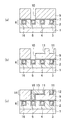
図1に示すように、半導体基板1の上には、炭素添加シリコン酸化膜(SiOC膜)である第1の絶縁膜2が形成され、第1の絶縁膜2の上部には、第1の配線溝3が形成されている。第1の配線溝3の側壁上及び底面上には、第1のバリア膜4が形成され、第1のバリア膜4の上には、第1の配線溝3を埋め込むように第1の銅(Cu)膜5が形成されて、下部配線6が形成されている。第1のCu膜5の上には、反応層であるケイ化銅(CuSix)層8が形成され、第1の絶縁膜2、第1のバリア膜4及びCuSix層8を覆うように、膜厚が約10nmのシリコン炭窒化膜(SiCN膜)である保護膜7が形成されている。保護膜7の上には、SiOC膜である第2の絶縁膜9が形成されている。一部のCuSix層8及びその周辺に形成されている第1のバリア膜4の上には、第2の絶縁膜9及び保護膜7を貫通し、下部配線6を露出するビアホール10が形成され、第2の絶縁膜9の上部には、複数の第2の配線溝11が形成されている。複数の第2の配線溝11の一部は、下部配線6を露出するビアホール10を有する。ビアホール10及び第2の配線溝11の側壁上及び底面上には、第2のバリア膜12が形成され、第2のバリア膜12の上には、ビアホール10及び第2の配線溝11を埋め込むように第2のCu膜13が形成されて、ビア及び上部配線14が形成されている。ここで、下部配線6と上部配線14とをビアが接続している。
As shown in FIG. 1, a first
本発明の第1の実施形態に係る半導体装置によると、配線の抵抗の増大を抑制すると共に、配線と周囲の膜との密着性を向上させるのに必要な厚さを有する反応層を備えるため、実用上十分なエレクトロマイグレーション耐性及び動作速度を得ることができる。 The semiconductor device according to the first embodiment of the present invention includes a reaction layer having a thickness necessary for suppressing an increase in wiring resistance and improving adhesion between the wiring and a surrounding film. Therefore, practically sufficient electromigration resistance and operation speed can be obtained.
次に、本発明の第1の実施形態に係る半導体装置の製造方法について、図2(a)〜(d)及び図3(a)〜(c)を参照しながら説明する。 Next, a method for manufacturing a semiconductor device according to the first embodiment of the present invention will be described with reference to FIGS. 2 (a) to 2 (d) and FIGS. 3 (a) to 3 (c).
まず、図2(a)に示すように、半導体基板1の上にSiOC膜である第1の絶縁膜2を形成し、リソグラフィ法及びドライエッチング法により、第1の絶縁膜2の上部に第1の配線溝3を形成する。
First, as shown in FIG. 2A, a first
次に、図2(b)に示すように、第1の絶縁膜2の上並びに第1の配線溝3の側壁上及び底面上に第1のバリア膜4及び第1のCu膜5を順次形成することにより、第1の配線溝3を埋め込む。続いて、第1の配線溝3の外部に形成された第1のバリア膜4及び第1のCu膜5を化学機械研磨(CMP)法により除去して、下部配線6を形成する。本実施形態において、下部配線6の最小線幅は約60nmとし、高さは約100nmに設定している。
Next, as shown in FIG. 2B, the
次に、図2(c)に示すように、第1の絶縁膜2、第1のバリア膜4及び第1のCu膜5を覆うように膜厚が約10nmのSiCN膜である保護膜7を形成する。
Next, as shown in FIG. 2C, the
次に、図2(d)に示すように、半導体基板1を400℃程度に加熱し、SiH4に暴露する。これにより、第1のCu膜5と保護膜7との界面に反応層であるCuSix層8が形成される。これは、SiH4が保護膜7の内部を拡散し、第1のCu膜5の表面に到達し、第1のCu膜5と反応するためである。このように、CuSix層8を形成することにより、従来技術と比較してCuSix層8の厚さを精度良く制御することができる。この理由に関しては、後に詳しく説明する。
Next, as shown in FIG. 2D, the
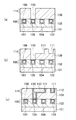
次に、図3(a)に示すように、保護膜7の上にSiOC膜である第2の絶縁膜9を形成し、リソグラフィ法及びドライエッチング法により、第2の絶縁膜9に保護膜7を露出するビアホール10を形成する。
Next, as shown in FIG. 3A, a second
次に、図3(b)に示すように、リソグラフィ法及びドライエッチング法により、第2の絶縁膜9の上部に複数の第2の配線溝11を形成すると共に、ビアホール10の底面の保護膜7を除去して、第1のバリア膜4及びCuSix層8を露出する。複数の第2の配線溝11の一部は、下部配線6を露出するビアホール10を有する。
Next, as shown in FIG. 3B, a plurality of
次に、図3(c)に示すように、第2の絶縁膜9の上、ビアホール10の側壁上及び底面上並びに第2の配線溝11の側壁上及び底面上に第2のバリア膜12及び第2のCu膜13を順次形成しビアホール10及び第2の配線溝11を埋め込む。その後、ビアホール10及び第2の配線溝11の外部の第2のバリア膜12及び第2のCu膜13をCMP法により除去して、ビア及び上部配線14を形成することにより、2層の配線を有する半導体装置が完成する。本実施形態では、上部配線14の最小線幅を約60nmとし、高さを約100nmに設定している。なお、図3(c)に示す工程の後、図2(c)〜図3(c)に示す工程を繰り返すことにより、任意の層数の配線を有する半導体装置を製造することもできる。
Next, as shown in FIG. 3C, the
本発明の第1の実施形態に係る半導体装置の製造方法によると、反応層であるCuSix層の厚さを精度良く制御できるため、実用上十分なエレクトロマイグレーション耐性及び動作速度を有する半導体装置を得ることができる。 According to the method for manufacturing a semiconductor device according to the first embodiment of the present invention, since the thickness of the CuSi x layer as a reaction layer can be accurately controlled, a semiconductor device having practically sufficient electromigration resistance and operation speed is obtained. Can be obtained.
ここで、本実施形態において、従来の技術と比較してCuSix層8の厚さを精度良く制御できる理由について説明する。一般に、Cu膜の表面において、SiH4は触媒作用により分解し、CuSix層が形成されることが知られている。300℃以下の低温において、この反応は反応律速であるため、形成されるCuSix層の厚さは、Cu膜の表面温度及び結晶状態に大きく影響される。一方、本実施形態では、第1のCu膜5の上に保護膜7を形成することにより、SiH4を保護膜7の内部に拡散し、第1のCu膜5の表面に供給するため、反応をSiH4の供給律速とすることができる。すなわち、形成されるCuSix層8の厚さは、第1のCu膜5の表面に到達するSiH4の量によって決まるため、第1のCu膜5の表面温度及び結晶状態に影響されない。以上の理由により、本実施形態では、従来の技術と比較してCuSix層8の厚さを精度良く制御することができる。
Here, in this embodiment, the reason why the thickness of the CuSi x layer 8 can be accurately controlled as compared with the conventional technique will be described. In general, it is known that SiH 4 is decomposed by a catalytic action on the surface of the Cu film to form a CuSi x layer. Since this reaction is reaction-limited at a low temperature of 300 ° C. or lower, the thickness of the formed CuSi x layer is greatly influenced by the surface temperature and crystal state of the Cu film. On the other hand, in the present embodiment, by forming the
なお、CuSix層8を形成する反応を供給律速とするには、前記の方法の他に、半導体基板1の加熱温度を例えば350℃程度に高く設定し、SiH4の分圧を例えば1mPa程度に低く設定した上で、保護膜7を形成せずに第1のCu膜5とSiH4とを直接接触させる方法もある。ただし、この方法では、CuSix層8の成長速度が大きく、半導体装置の製造に必要な数nmの厚さのCuSix層8を制御性良く形成することは困難であるため、前記のように保護膜7を介してSiH4を供給する方法が好ましい。
In addition, in order to make the reaction for forming the CuSi x layer 8 rate-limiting, in addition to the above method, the heating temperature of the
前記のように、保護膜7の役割は、第1のCu膜5の表面に到達するSiH4の量を適切に制御することであるため、保護膜7は、SiH4が通過できる程度の径の細孔を有している必要がある。また、保護膜7は、第1の絶縁膜2、第1のCu膜5及び第2の絶縁膜9に対し、化学的に不活性であり、適度な密着性を有することも必要である。これらを満足する材料としては、CH3基を不純物として含むSiCNが挙げられる。このようなSiCNからなる保護膜7は、テトラメチルシラン(tetramethylsilane:TMS)及びアンモニア(NH3)を原料ガスとして用いるプラズマ化学気相成長(Chemical Vapor Deposition:CVD)法により得ることができる。また、保護膜7の膜厚は、2.5nmよりも薄くなると、ピンホール等に起因するCuSix層8の異常成長の頻度が上昇してしまう。一方、保護膜7の膜厚が20nmよりも厚くなると、第1のCu膜5の表面にSiH4が到達する量が極端に減少し、CuSix層8が成長する速度が極端に低下してしまう。従って、保護膜7の膜厚は、2.5nm以上且つ20nm以下程度に設定することが好ましい。そこで、本実施形態では、保護膜7として膜厚が約10nmのSiCN膜を用いている。
As described above, since the role of the
次に、図2(d)に示す工程における、半導体基板1の好ましい加熱温度について説明する。加熱温度を300℃よりも低く設定すると、SiH4が保護膜7の内部を拡散する速度が低下するため、十分な厚さのCuSix層8が得られない。また、加熱温度を400℃よりも高く設定すると、SiH4の分解反応のために保護膜7の表面にSi層が形成される。従って、加熱温度は、300℃以上且つ400℃以下程度に設定することが好ましいため、本実施形態では加熱温度を400℃程度としている。
Next, a preferable heating temperature of the
次に、図2(d)に示す工程における、CuSix層8の好ましい厚さについて説明する。CuSix層8の厚さが2nmよりも小さくなると、CuSix層8の連続性を保つことが困難となり、第1のCu膜5と保護膜7との密着性が低下する。また、CuSix層8の厚さが10nmよりも大きくなると、下部配線6の抵抗が上昇し、半導体装置の動作速度が低下する。従って、CuSix層8の厚さは、2nm以上且つ10nm以下程度に設定することが好ましい。
Next, a preferable thickness of the CuSi x layer 8 in the step shown in FIG. When the thickness of the CuSi x layer 8 is smaller than 2 nm, it becomes difficult to maintain the continuity of the CuSi x layer 8, and the adhesion between the
(第1の実施形態の第1の変形例)
以下、本発明の第1の実施形態の第1の変形例に係る半導体装置について、図4を参照しながら説明する。第1の実施形態の第1の変形例の半導体装置において、第1の実施形態の半導体装置における図1に示す部材と同一の部材については、同一の符号を付与することにより説明を省略し、第1の実施形態と異なる点について説明する。
(First modification of the first embodiment)
Hereinafter, a semiconductor device according to a first modification of the first embodiment of the present invention will be described with reference to FIG. In the semiconductor device of the first modification of the first embodiment, the same members as those shown in FIG. 1 in the semiconductor device of the first embodiment will be omitted by giving the same reference numerals. Differences from the first embodiment will be described.
図4に示すように、第1のCu膜5の上に反応層16が形成され、反応層16の上に保護膜7が形成されている点が第1の実施形態と異なる。反応層16は、CuSixとNiSixとの混合物からなる。このように、反応層16を形成することにより、第1の実施形態と比較して、第1のCu膜5と保護膜7の密着性がさらに向上するため、エレクトロマイグレーション耐性をさらに向上させることができる。
As shown in FIG. 4, the
本発明の第1の実施形態の第1の変形例に係る半導体装置によると、配線の抵抗の増大を抑制すると共に、配線と周囲の膜との密着性を向上させるのに必要な厚さを有する反応層を備えるため、実用上十分なエレクトロマイグレーション耐性及び動作速度を得ることができる。 According to the semiconductor device according to the first modification of the first embodiment of the present invention, the thickness necessary for suppressing the increase in the resistance of the wiring and improving the adhesion between the wiring and the surrounding film is increased. Since the reaction layer is provided, practically sufficient electromigration resistance and operation speed can be obtained.
以下、本発明の第1の実施形態の第1の変形例に係る半導体装置の製造方法について、図5(a)〜(c)及び図6(a)〜(c)を参照しながら説明する。なお、図5(a)〜(c)及び図6(a)〜(c)において、第1の実施形態における図2(a)〜(d)及び図3(a)〜(c)に示す部材と同一の部材については、同一の符号を付与することにより説明を省略する。また、第1の実施形態の第1の変形例において、半導体基板1〜下部配線6を形成するまでの工程は、第1の実施形態と同一であるため説明を省略する。
Hereinafter, a method for manufacturing a semiconductor device according to a first modification of the first embodiment of the present invention will be described with reference to FIGS. 5 (a) to 5 (c) and FIGS. 6 (a) to 6 (c). . 5A to 5C and FIGS. 6A to 6C are shown in FIGS. 2A to 2D and FIGS. 3A to 3C in the first embodiment. About the member same as a member, description is abbreviate | omitted by providing the same code | symbol. Further, in the first modification of the first embodiment, the steps from the formation of the
まず、図5(a)に示すように、第1のCu膜5の上部に被覆層15を形成する。ここで、被覆層15は、第1のCu膜5の表面に選択的に形成でき、且つ、SiH4と反応して安定な化合物を生成することが必要である。これらを満足する材料としては、ニッケル(Ni)膜、Ni合金膜、コバルト(Co)膜及びCo合金膜等が知られている。これらは、無電解メッキ法により第1のCu膜5の表面に選択的に形成することができる。本実施形態において、被覆層15は、無電解メッキ法により析出させたNi層である。
First, as shown in FIG. 5A, a
次に、図5(b)に示すように、第1の絶縁膜2、第1のバリア膜4及び被覆層15を覆うように保護膜7を形成する。
Next, as shown in FIG. 5B, a
次に、図5(c)に示すように、半導体基板1を加熱し、SiH4に暴露する。これにより、第1のCu膜5と保護膜7との界面に反応層16が形成される。本実施形態の場合、反応層16は、CuSixとNiSixとの混合物からなる。このように、反応層16を形成することにより、第1の実施形態と比較して、第1のCu膜5と保護膜7の密着性がさらに向上するため、エレクトロマイグレーション耐性をさらに向上させることができる。
Next, as shown in FIG. 5C, the
次に、図6(a)〜図6(c)に示すように、第1の実施形態と同様に、保護膜7の上に第2の絶縁膜9を形成し、第2の絶縁膜9にビアホール10及び第2の配線溝11を形成した後、ビアホール10及び第2の配線溝11を埋め込むように第2のバリア膜12及び第2のCu膜13を順次形成して、ビア及び上部配線14を形成する。なお、図6(c)に示す工程の後、図5(b)〜図6(c)に示す工程を繰り返すことにより、任意の層数の配線を有する半導体装置を製造することもできる。
Next, as shown in FIG. 6A to FIG. 6C, as in the first embodiment, a second
本発明に係る第1の実施形態の第1の変形例によると、反応層であるCuSixとNiSixとの混合物からなる層の厚さを精度良く制御できるため、実用上十分なエレクトロマイグレーション耐性及び動作速度を有する半導体装置を得ることができる。 According to the first modification of the first embodiment of the present invention, the thickness of a layer made of a mixture of CuSi x and NiSi x that is a reaction layer can be controlled with high accuracy, so that electromigration resistance sufficient for practical use is achieved. In addition, a semiconductor device having an operation speed can be obtained.
(第1の実施形態の第2の変形例)
以下、本発明の第1の実施形態の第2の変形例について、図7(a)〜(d)を参照しながら説明する。なお、図7(a)〜(d)において、第1の実施形態における図2(a)〜(d)及び図3(a)〜(c)に示す部材と同一の部材については、同一の符号を付与することにより説明を省略する。また、第1の実施形態の第2の変形例において、半導体基板1〜CuSix層8を形成するまでの工程は第1の実施形態と同一であるため説明を省略する。
(Second modification of the first embodiment)
Hereinafter, a second modification of the first embodiment of the present invention will be described with reference to FIGS. 7A to 7D, the same members as those shown in FIGS. 2A to 2D and FIGS. 3A to 3C in the first embodiment are the same. The description is omitted by assigning a reference numeral. Further, in the second modification of the first embodiment, the steps until the
まず、図7(a)に示すように、保護膜7の表面をNH3プラズマに暴露する。これにより、第1のCu膜5、保護膜7及びCuSix層8の相互拡散が促進され、第1のCu膜5と保護膜7との密着性が向上するため、第1の実施形態と比較してエレクトロマイグレーション耐性を向上させることができる。ここで、この効果を確実に得るためには、保護膜7の表面に、窒素(N2)、ジアゼン(HN=NH)及びヒドラジン(H2N−NH2)等の窒素化合物を含む雰囲気中において発生させたプラズマを照射することが好ましい。また、他の好ましい方法としては、保護膜7の表面に紫外光を照射することが挙げられる。
First, as shown in FIG. 7A, the surface of the
次に、図7(b)〜図7(d)に示すように、第1の実施形態と同様に、保護膜7の上に第2の絶縁膜9を形成し、第2の絶縁膜9にビアホール10及び第2の配線溝11を形成した後、ビアホール10及び第2の配線溝11を埋め込むように第2のバリア膜12及び第2のCu膜13を順次形成して、ビア及び上部配線14を形成する。なお、図7(d)に示す工程の後、図2(c)、図2(d)及び図7(a)〜図7(d)に示す工程を繰り返すことにより、任意の層数の配線を有する半導体装置を製造することもできる。
Next, as shown in FIGS. 7B to 7D, the second
本実施形態は、第1の実施形態に対して工程を追加した例であるが、第1の実施形態の第1の変形例に対しても同様に適用することができる。 Although this embodiment is an example in which a process is added to the first embodiment, the present embodiment can be similarly applied to the first modification of the first embodiment.
本発明に係る第1の実施形態の第2の変形例によると、反応層であるCuSix層の厚さを精度良く制御できるため、実用上十分なエレクトロマイグレーション耐性及び動作速度を有する半導体装置を得ることができる。 According to the second modification of the first embodiment of the present invention, since the thickness of the CuSi x layer that is the reaction layer can be controlled with high accuracy, a semiconductor device having practically sufficient electromigration resistance and operation speed can be obtained. Can be obtained.
(第2の実施形態)
以下、本発明の第2の実施形態に係る半導体装置について、図8を参照しながら説明する。第2の実施形態の半導体装置は、第1の実施形態の半導体装置における図1に示す半導体基板1〜下部配線6及びCuSix層8の構造と同一であるため、説明を省略する。
(Second Embodiment)
A semiconductor device according to the second embodiment of the present invention will be described below with reference to FIG. The semiconductor device of the second embodiment is the same as the structure of the
図8に示すように、第1の絶縁膜2、第1のバリア膜4及びCuSix層8を覆うように、膜厚が約5nmのシリコン炭窒化膜(SiCN)である保護膜17が形成されている。保護膜17の上には、膜厚が約20nmの酸素添加シリコン炭化膜(SiCO膜)であるストッパ膜18が形成されている。ストッパ膜18の上には、SiOC膜である第2の絶縁膜9が形成されている。一部のCuSix層8及びその周辺に形成されている第1のバリア膜4の上には、第2の絶縁膜9、ストッパ膜18及び保護膜17を貫通し、CuSix層8及び第1のバリア膜4を露出するビアホール10が形成され、第2の絶縁膜9の上部には、第2の配線溝11が形成されている。ビアホール10及び第2の配線溝11の側壁上及び底面上には、第2のバリア膜12が形成され、第2のバリア膜12の上には、ビアホール10及び第2の配線溝11を埋め込むように第2のCu膜13が形成されて、ビア及び上部配線14が形成されている。ここで、下部配線6と上部配線14とをビアが接続している。
As shown in FIG. 8, a
第2の絶縁膜9の材料によっては、ビアホール10を形成する際にビアホール10の底部に下部配線6を露出させず、第2の配線溝11を形成する際に下部配線6を露出させる方が、歩留りが良好な場合がある。これを安定して実現するために、本実施形態では、第2の絶縁膜9に対してエッチング選択比の大きいストッパ膜18を形成している。
Depending on the material of the second
本発明の第2の実施形態に係る半導体装置によると、配線の抵抗の増大を抑制すると共に、配線と周囲の膜との密着性を向上させるのに必要な厚さを有する反応層を備えるため、実用上十分なエレクトロマイグレーション耐性及び動作速度を得ることができる。 The semiconductor device according to the second embodiment of the present invention includes a reaction layer having a thickness necessary for suppressing an increase in wiring resistance and improving adhesion between the wiring and a surrounding film. Therefore, practically sufficient electromigration resistance and operation speed can be obtained.
以下、本発明の第2の実施形態に係る半導体装置の製造方法について、図9(a)〜(c)及び図10(a)〜(c)を参照しながら説明する。なお、図9(a)〜(c)及び図10(a)〜(c)において、第1の実施形態における図2(a)〜(d)及び図3(a)〜(c)に示す部材と同一の部材については、同一の符号を付与することにより説明を省略する。また、第2の実施形態において、半導体基板1〜下部配線6を形成するまでの工程は第1の実施形態と同一であるため説明を省略する。
A semiconductor device manufacturing method according to the second embodiment of the present invention will be described below with reference to FIGS. 9 (a) to 9 (c) and FIGS. 10 (a) to 10 (c). In addition, in FIG. 9 (a)-(c) and FIG. 10 (a)-(c), it shows to FIG. 2 (a)-(d) and FIG. 3 (a)-(c) in 1st Embodiment. About the member same as a member, description is abbreviate | omitted by providing the same code | symbol. Further, in the second embodiment, the steps from the formation of the
まず、図9(a)に示すように、第1の絶縁膜2、第1のバリア膜4及び第1のCu膜5の上に、膜厚が約5nmのSiCN膜である保護膜17を形成する。
First, as shown in FIG. 9A, a
次に、図9(b)に示すように、半導体基板1を加熱し、SiH4に暴露する。これにより、第1のCu膜5と保護膜17との界面に反応層であるCuSix層8が形成される。
Next, as shown in FIG. 9B, the
次に、図9(c)に示すように、保護膜17の上にストッパ膜18を形成する。ここで、ストッパ膜18の材料として、SiCO又は窒化シリコン(SiN)を用いることが好ましい。SiCOは、テトラメチルシラン(TMS)及び二酸化炭素(CO2)を原料ガスとして用いたプラズマCVD法により得ることができ、SiNはシラン及びNH3を原料ガスとして用いたプラズマCVD法により得ることができる。本実施形態では、ストッパ膜18は、膜厚が約20nmのSiCO膜を用いている。
Next, as shown in FIG. 9C, a
次に、図10(a)に示すように、ストッパ膜18の上に第2の絶縁膜9を形成する。
Next, as shown in FIG. 10A, the second
次に、図10(b)に示すように、第2の絶縁膜9の内部にビアホール10を形成する。このとき、ビアホール10のエッチングは、第2の絶縁膜9と比べて、ストッパ膜18の方がエッチングレートが低い条件で行い、ストッパ膜18の表面においてエッチングを停止する。
Next, as shown in FIG. 10B, a via
第2の絶縁膜9の材料によっては、ビアホール10を形成する際にビアホール10の底部に下部配線6を露出させず、第2の配線溝11を形成する際に下部配線6を露出させる方が、歩留りが良好な場合がある。これを安定して実現するためには、第2の絶縁膜9に対してエッチング選択比の大きいストッパ膜18を形成し、ビアホール10の形成のためのエッチングをストッパ膜18が露出するまで行うことが有効である。
Depending on the material of the second
次に、図10(c)に示すように、第2の絶縁膜9の上部に複数の第2の配線溝11を形成すると共に、ビアホール10の底部の保護膜17及びストッパ膜18を除去した後、ビアホール10及び第2の配線溝11を埋め込むように第2のバリア膜12及び第2のCu膜13を順次形成して、ビア及び上部配線14を形成する。なお、図10(c)に示す工程の後、図9(a)〜図9(c)及び図10(a)〜図10(c)に示す工程を繰り返すことにより、任意の層数の配線を有する半導体装置を製造することもできる。
Next, as shown in FIG. 10C, a plurality of
本実施形態は、第1の実施形態に対してストッパ膜18を形成する工程を追加した例であるが、第1の実施形態の第1の変形例及び第2の変形例に対しても適用できる。
The present embodiment is an example in which a step of forming the
本発明に係る第2の半導体装置の製造方法によると、反応層であるCuSix層の厚さを精度良く制御できるため、実用上十分なエレクトロマイグレーション耐性及び動作速度を有する半導体装置を得ることができる。 According to the second method for manufacturing a semiconductor device according to the present invention, the thickness of the CuSi x layer as the reaction layer can be controlled with high accuracy, so that a semiconductor device having practically sufficient electromigration resistance and operating speed can be obtained. it can.
以上、本発明の実施形態及びその変形例について説明してきたが、本発明はそれらに限定されるものではない。 As mentioned above, although embodiment of this invention and its modification were demonstrated, this invention is not limited to them.
例えば、前記の実施形態では、CuSix層8又は反応層16の形成にSiH4を用いているが、ポリシラン(SinH2n+2)等のシリコン化合物を代わりに用いることができる。さらに、これらのシリコン化合物の代わりに、ゲルマン(GeH4)及びポリゲルマン(GenH2n+2)等のゲルマニウム化合物を代わりに用いることもできる。この場合、CuSix層の代わりにゲルマニウム化銅(CuGex)層が形成され、反応層16はYGexとCuGexとの混合物となる。ただし、YはNi又はCoのいずれかである。
For example, in the above-described embodiment, SiH 4 is used to form the CuSi x layer 8 or the
また、前記の実施形態では、CuSix層8又は反応層16の形成のために、保護膜7の表面をSiH4等の反応性ガスに暴露しているが、反応性ガスを化学的もしくは物理的に活性化する手段をさらに備えていても良い。前者の例としては、反応装置の内部又は外部におけるプラズマによる反応性ガスのラジカル化又はイオン化が挙げられる。また、後者の例としては、イオン注入技術の適用による反応性ガスへの運動エネルギーの付与が挙げられる。
In the above embodiment, the surface of the
また、前記の実施形態では、第1のCu膜5を用いて下部配線6を形成しているが、Cu合金膜、アルミニウム(Al)膜、Al合金膜、銀(Ag)膜、Ag合金膜、金(Au)膜及びAu合金膜等を用いて下部配線6を形成することも可能である。これらの場合には、CuSix層の代わりにXSix層が形成され、反応層16はYGexとCuGexとの混合物となる。ただし、Xは下部配線の主要な構成元素であり、YはNi又はCoのいずれかである。
In the above embodiment, the
また、前記の実施形態では、第2の配線溝11よりも先にビアホール10を形成しているが、逆に、ビアホール10よりも先に第2の配線溝11を形成することも可能である。
In the above-described embodiment, the via
その他、本発明は、本発明の趣旨を逸脱しない範囲において、種々の形態に変形して適用可能である。 In addition, the present invention can be modified and applied in various forms without departing from the spirit of the present invention.
本発明に係る半導体装置及びその製造方法は、反応層の膜厚を精度良く制御することが可能となるため、実用上十分なエレクトロマイグレーション耐性及び動作速度を得ることができ、特に、埋め込み型の配線構造を有する半導体装置及びその製造方法等に有用である。 Since the semiconductor device and the manufacturing method thereof according to the present invention can accurately control the thickness of the reaction layer, it is possible to obtain practically sufficient electromigration resistance and operation speed. This is useful for a semiconductor device having a wiring structure and a method for manufacturing the same.
1 半導体基板
2 第1の絶縁膜
3 第1の配線溝
4 第1のバリア膜
5 第1の銅(Cu)膜
6 下部配線
7 保護膜
8 ケイ化銅(CuSix)層(反応層)
9 第2の絶縁膜
10 ビアホール
11 第2の配線溝
12 第2のバリア膜
13 第2の銅(Cu)膜
14 上部配線
15 被覆層
16 反応層
17 保護膜
18 ストッパ膜
1
9 Second insulating
Claims (16)
前記第1の絶縁膜に配線溝を形成する工程(b)と、
前記配線溝に第1の配線を形成する工程(c)と、
前記第1の絶縁膜及び第1の配線の上に保護膜を形成する工程(d)と、
前記工程(d)よりも後に、前記保護膜の表面に反応性ガスを暴露することにより、前記第1の配線と前記保護膜との界面に反応層を形成する工程(e)とを備え、
前記工程(e)は、シリコン化合物又はゲルマニウム化合物を前記保護膜の表面に暴露することにより行われることを特徴とする半導体装置の製造方法。 Forming a first insulating film on the semiconductor substrate (a);
Forming a wiring trench in the first insulating film (b);
Forming a first wiring in the wiring groove (c);
A step (d) of forming a protective film on the first insulating film and the first wiring;
A step (e) of forming a reaction layer at the interface between the first wiring and the protective film by exposing a reactive gas to the surface of the protective film after the step (d) ;
The method (e) is performed by exposing a silicon compound or a germanium compound to the surface of the protective film .
前記第2の絶縁膜の内部にビアホールを形成する工程(g)と、
前記ビアホールと接続するように第2の配線を形成する工程(h)とをさらに備えていることを特徴とする請求項1〜5のうちのいずれか1項に記載の半導体装置の製造方法。 A step (f) of forming a second insulating film on the protective film;
Forming a via hole in the second insulating film (g);
The method of manufacturing a semiconductor device of any one of claims 1 to 5, characterized by further comprising a step (h) forming second wiring so as to connect to the via holes.
Priority Applications (3)
| Application Number | Priority Date | Filing Date | Title |
|---|---|---|---|
| JP2009148054A JP5230542B2 (en) | 2009-06-22 | 2009-06-22 | Manufacturing method of semiconductor device |
| PCT/JP2010/000444 WO2010150430A1 (en) | 2009-06-22 | 2010-01-27 | Semiconductor device and process for manufacture thereof |
| US13/274,039 US8927416B2 (en) | 2009-06-22 | 2011-10-14 | Semiconductor device and method of manufacturing the same |
Applications Claiming Priority (1)
| Application Number | Priority Date | Filing Date | Title |
|---|---|---|---|
| JP2009148054A JP5230542B2 (en) | 2009-06-22 | 2009-06-22 | Manufacturing method of semiconductor device |
Publications (3)
| Publication Number | Publication Date |
|---|---|
| JP2011003859A JP2011003859A (en) | 2011-01-06 |
| JP2011003859A5 JP2011003859A5 (en) | 2011-08-18 |
| JP5230542B2 true JP5230542B2 (en) | 2013-07-10 |
Family
ID=43386221
Family Applications (1)
| Application Number | Title | Priority Date | Filing Date |
|---|---|---|---|
| JP2009148054A Expired - Fee Related JP5230542B2 (en) | 2009-06-22 | 2009-06-22 | Manufacturing method of semiconductor device |
Country Status (3)
| Country | Link |
|---|---|
| US (1) | US8927416B2 (en) |
| JP (1) | JP5230542B2 (en) |
| WO (1) | WO2010150430A1 (en) |
Families Citing this family (3)
| Publication number | Priority date | Publication date | Assignee | Title |
|---|---|---|---|---|
| US20160276156A1 (en) * | 2015-03-16 | 2016-09-22 | Taiwan Semiconductor Manufacturing Company Ltd. | Semiconductor device and manufacturing process thereof |
| US9673091B2 (en) * | 2015-06-25 | 2017-06-06 | Globalfoundries Inc. | Structure for BEOL metal levels with multiple dielectric layers for improved dielectric to metal adhesion |
| CN112151497B (en) * | 2019-06-28 | 2023-08-22 | 台湾积体电路制造股份有限公司 | Semiconductor structure and method for forming semiconductor structure |
Family Cites Families (9)
| Publication number | Priority date | Publication date | Assignee | Title |
|---|---|---|---|---|
| KR19980042910A (en) | 1996-11-29 | 1998-08-17 | 윌리엄비.켐플러 | Process for sealing the copper surface |
| US6448655B1 (en) * | 1998-04-28 | 2002-09-10 | International Business Machines Corporation | Stabilization of fluorine-containing low-k dielectrics in a metal/insulator wiring structure by ultraviolet irradiation |
| JP2000058544A (en) * | 1998-08-04 | 2000-02-25 | Matsushita Electron Corp | Semiconductor device and manufacture of the same |
| JP4535629B2 (en) * | 2001-02-21 | 2010-09-01 | ルネサスエレクトロニクス株式会社 | Manufacturing method of semiconductor device |
| JP4063619B2 (en) * | 2002-03-13 | 2008-03-19 | Necエレクトロニクス株式会社 | Manufacturing method of semiconductor device |
| US20050250346A1 (en) * | 2004-05-06 | 2005-11-10 | Applied Materials, Inc. | Process and apparatus for post deposition treatment of low k dielectric materials |
| KR100703973B1 (en) * | 2005-07-20 | 2007-04-06 | 삼성전자주식회사 | Interconnections having double story capping layer and method for forming the same |
| JP2009016502A (en) * | 2007-07-03 | 2009-01-22 | Tdk Corp | Wire coating separation method, manufacturing method of coil component, wire coating separation device, and manufacturing device of coil component |
| JP2009016520A (en) * | 2007-07-04 | 2009-01-22 | Tokyo Electron Ltd | Method and apparatus for manufacturing semiconductor apparatus |
-
2009
- 2009-06-22 JP JP2009148054A patent/JP5230542B2/en not_active Expired - Fee Related
-
2010
- 2010-01-27 WO PCT/JP2010/000444 patent/WO2010150430A1/en active Application Filing
-
2011
- 2011-10-14 US US13/274,039 patent/US8927416B2/en active Active
Also Published As
| Publication number | Publication date |
|---|---|
| US8927416B2 (en) | 2015-01-06 |
| JP2011003859A (en) | 2011-01-06 |
| WO2010150430A1 (en) | 2010-12-29 |
| US20120032333A1 (en) | 2012-02-09 |
Similar Documents
| Publication | Publication Date | Title |
|---|---|---|
| TWI446487B (en) | Increasing reliability of copper-based metallization structures in a microstructure device by using aluminum nitride | |
| JP5500810B2 (en) | Method for forming voids in a multilayer wiring structure | |
| US7833901B2 (en) | Method for manufacturing a semiconductor device having a multi-layered insulating structure of SiOCH layers and an SiO2 layer | |
| CN101728319B (en) | Circuit structure of metal line modified through silicon/germanium soaking | |
| US7413985B2 (en) | Method for forming a self-aligned nitrogen-containing copper silicide capping layer in a microstructure device | |
| KR100602087B1 (en) | Semiconductor device and method of manufacturing the same | |
| JP2015177006A (en) | Semiconductor device and manufacturing method of the same | |
| JP2009515319A (en) | Manufacturing method of structure for semiconductor device | |
| JP5230542B2 (en) | Manufacturing method of semiconductor device | |
| JP5217272B2 (en) | Wiring forming method and semiconductor device manufacturing method | |
| JP2007157959A (en) | Method of manufacturing semiconductor device, and semiconductor device | |
| KR101152203B1 (en) | Semiconductor device and manufacturing method therefor | |
| KR101430832B1 (en) | Apparatus and method for low contact resistance carbon nanotube interconnect | |
| JP2007258390A (en) | Semiconductor device and manufacturing method therefor | |
| US10186454B2 (en) | Semiconductor structure having etch stop layer and method of forming the same | |
| JP2010080607A (en) | Method of manufacturing semiconductor device | |
| US7902641B2 (en) | Semiconductor device and manufacturing method therefor | |
| JP2011029554A (en) | Method of manufacturing semiconductor device | |
| JP2010073736A (en) | Method of manufacturing semiconductor device | |
| JP2010080606A (en) | Method of manufacturing semiconductor apparatus | |
| KR20060011396A (en) | Method for forming multi layer metal line in semiconductor device | |
| CN112435958A (en) | Integrated circuit structure and forming method thereof | |
| Ohto et al. | Method for manufacturing a semiconductor device having a multi-layered insulating structure of SiOCH layers and an SiO 2 layer | |
| US20090136724A1 (en) | Method of fabricating semiconductor device |
Legal Events
| Date | Code | Title | Description |
|---|---|---|---|
| A521 | Request for written amendment filed |
Free format text: JAPANESE INTERMEDIATE CODE: A523 Effective date: 20110704 |
|
| RD02 | Notification of acceptance of power of attorney |
Free format text: JAPANESE INTERMEDIATE CODE: A7422 Effective date: 20120210 |
|
| A131 | Notification of reasons for refusal |
Free format text: JAPANESE INTERMEDIATE CODE: A131 Effective date: 20121211 |
|
| A521 | Request for written amendment filed |
Free format text: JAPANESE INTERMEDIATE CODE: A523 Effective date: 20130130 |
|
| TRDD | Decision of grant or rejection written | ||
| A01 | Written decision to grant a patent or to grant a registration (utility model) |
Free format text: JAPANESE INTERMEDIATE CODE: A01 Effective date: 20130219 |
|
| A61 | First payment of annual fees (during grant procedure) |
Free format text: JAPANESE INTERMEDIATE CODE: A61 Effective date: 20130319 |
|
| FPAY | Renewal fee payment (event date is renewal date of database) |
Free format text: PAYMENT UNTIL: 20160329 Year of fee payment: 3 |
|
| R150 | Certificate of patent or registration of utility model |
Ref document number: 5230542 Country of ref document: JP Free format text: JAPANESE INTERMEDIATE CODE: R150 Free format text: JAPANESE INTERMEDIATE CODE: R150 |
|
| S111 | Request for change of ownership or part of ownership |
Free format text: JAPANESE INTERMEDIATE CODE: R313113 |
|
| R350 | Written notification of registration of transfer |
Free format text: JAPANESE INTERMEDIATE CODE: R350 |
|
| R250 | Receipt of annual fees |
Free format text: JAPANESE INTERMEDIATE CODE: R250 |
|
| LAPS | Cancellation because of no payment of annual fees |