EP1341259A1 - Geschichtete Streifenleitungsantenne für mehrere Frequenzen mit verbesserter Frequenzbandisolation - Google Patents
Geschichtete Streifenleitungsantenne für mehrere Frequenzen mit verbesserter Frequenzbandisolation Download PDFInfo
- Publication number
- EP1341259A1 EP1341259A1 EP03250716A EP03250716A EP1341259A1 EP 1341259 A1 EP1341259 A1 EP 1341259A1 EP 03250716 A EP03250716 A EP 03250716A EP 03250716 A EP03250716 A EP 03250716A EP 1341259 A1 EP1341259 A1 EP 1341259A1
- Authority
- EP
- European Patent Office
- Prior art keywords
- patch
- antenna
- conductor
- antennas
- radiating
- Prior art date
- Legal status (The legal status is an assumption and is not a legal conclusion. Google has not performed a legal analysis and makes no representation as to the accuracy of the status listed.)
- Granted
Links
Images


Classifications
-
- H—ELECTRICITY
- H01—ELECTRIC ELEMENTS
- H01Q—ANTENNAS, i.e. RADIO AERIALS
- H01Q21/00—Antenna arrays or systems
- H01Q21/28—Combinations of substantially independent non-interacting antenna units or systems
-
- H—ELECTRICITY
- H01—ELECTRIC ELEMENTS
- H01Q—ANTENNAS, i.e. RADIO AERIALS
- H01Q5/00—Arrangements for simultaneous operation of antennas on two or more different wavebands, e.g. dual-band or multi-band arrangements
- H01Q5/30—Arrangements for providing operation on different wavebands
- H01Q5/378—Combination of fed elements with parasitic elements
- H01Q5/385—Two or more parasitic elements
-
- H—ELECTRICITY
- H01—ELECTRIC ELEMENTS
- H01Q—ANTENNAS, i.e. RADIO AERIALS
- H01Q5/00—Arrangements for simultaneous operation of antennas on two or more different wavebands, e.g. dual-band or multi-band arrangements
- H01Q5/40—Imbricated or interleaved structures; Combined or electromagnetically coupled arrangements, e.g. comprising two or more non-connected fed radiating elements
-
- H—ELECTRICITY
- H01—ELECTRIC ELEMENTS
- H01Q—ANTENNAS, i.e. RADIO AERIALS
- H01Q9/00—Electrically-short antennas having dimensions not more than twice the operating wavelength and consisting of conductive active radiating elements
- H01Q9/04—Resonant antennas
- H01Q9/0407—Substantially flat resonant element parallel to ground plane, e.g. patch antenna
- H01Q9/0414—Substantially flat resonant element parallel to ground plane, e.g. patch antenna in a stacked or folded configuration
Definitions
- the invention pertains to stacked patch antennas. More particularly, the invention pertains to stacked patch antennas with improved frequency band isolation and multiple (greater than two) frequency bands of operation.
- a patch antenna is a type of antenna that is particularly suitable for relatively narrow band operation.
- a patch antenna usually comprises a dielectric panel with conductive patterns or patches deposited on both sides of the dielectric panel.
- the top conductive pattern or patch is the radiator and is sized and shaped to resonate at a particular frequency.
- This top patch (hereinafter termed the radiating patch of the patch antenna) acts as a parallel plane, micro strip transmission line serving as an antenna by giving in-phase linearly or circularly polarized radiation.
- the radiating patch is fed, for example, by a coaxial feed.
- a coaxial feed comprises a central conductor encircled concentrically by a dielectric, with the dielectric encircled concentrically by another, outer conductor serving as a shield.
- the outer conductor typically is connected to a ground plane.
- the inner conductor is connected to the radiating patch.
- the signal whether transmitted from the antenna or received by the antenna, travels as a voltage differential between the inner conductor and the outer, grounded conductor.
- the radiating patch radiates the signal from its edges.
- the bottom conductive pattern acts as a ground plane for the radiating patch and is hereinafter termed the ground patch of the patch antenna.
- patch antennas are extremely compact. However, they usually radiate efficiently over only a fairly narrow bandwidth. Accordingly, they are most commonly used in narrow bandwidth applications, such as GPS (global positioning satellite) systems, which operates over one or two very narrow frequency bands.
- GPS global positioning satellite
- the GPS system operates in two distinct bandwidths, a military band at 1227 MHZ and a civilian band at 1575 MHZ.
- GPS receivers that are allowed to access the military bandwidth (and thus operate with much higher accuracy) actually access the signals on both bandwidths. Accordingly, such systems would require two patch antennas, each designed to resonate in one of the two frequency bands.
- a known method of feeding the radiating patch is to connect the inner conductor of the coaxial feed to the patch at a natural feed point of the patch.
- the natural feed point of the radiating patch is the point at which it presents an apparent fifty ohm impedance when a conductor is coupled at that point. This locus of points typically is offset from the geometric center of the radiating patch.
- Stacked patch antennas are known in which two patch antennas are stacked on top of each other.
- the individual antennas in a stacked patched antenna assembly will be referred to as patch antennas or simply antennas.
- the top conductive pattern of a patch antenna will be termed the radiating patch of the patch antenna and the bottom conductive pattern, if included, will be termed the ground patch of the patch antenna.
- the entire stacked patch antenna assembly comprising multiple patch antennas will be referred to as a stacked patch antenna assembly.
- a stacked patch antenna assembly is suitable for the aforementioned two band GPS type application.
- Conventional stacked patch antenna assemblies typically have used one of two types of feed arrangements. In one arrangement, only one patch antenna is directly fed while the other is parasitically coupled to the first patch antenna. In the other type of feed arrangement, each patch antenna is directly fed. In the type of feed arrangement where each patch antenna is directly fed, each feed, which comprises a coaxial cable with an inner and an outer conductor, has the outer conductor shorted to the ground patch at some non-centered point on the patch antenna.
- FIG. 5 discloses a stacked patch antenna assembly with improved frequency band isolation.
- That patent discloses an exemplary stacked patch antenna assembly in which two patch antennas are fed by separate conductors.
- a coaxial feed for the upper patch antenna runs through an aperture in the lower patch antenna that is coincident with the null point of the lower patch antenna.
- the inner conductor electrically couples to the null point of the radiating patch of the uppermost patch antenna.
- the outer conductor of the coaxial feed cable for the upper patch antenna is electrically connected to both the ground plane and the lower patch antenna.
- the outer conductor of the coaxial feed presents to the radiating patch of the upper antenna an inductance to ground referenced at a ground plane.
- the lower patch antenna is fed by a separate coaxial conductor that is coupled to a natural feed point of the radiating patch of the lower patch antenna.
- an object of the present invention to provide an improved stacked patch antenna assembly.
- Other objects are to provide a stacked patch antenna assembly with improved frequency band isolation and/or to provide a stacked patch antenna assembly with pattern diversity.
- the invention is a multiple stacked patch antenna assembly in which the number of possible patch antennas is theoretically unlimited and which provides excellent isolation between the frequency bands.
- an exemplary antenna assembly with four antennas four patch antennas are stacked above a ground plane with the radiating patch of each patch antenna (other than the uppermost antenna) serving a secondary purpose of acting as a ground plane for the patch antenna above it.
- the aforementioned ground plane serves as the ground plane of the lowest antenna in the stack.
- a single coaxial cable feeds the two uppermost patch antennas, with the radiating patch of the uppermost patch antenna coupled at its null point to the inner conductor.
- the upper antenna also may contain an etched transmission line to obtain the "natural feed point," if other than annular radiation is desired, as discussed in further detail below.
- the radiating patch of the second uppermost patch antenna is parasitically coupled through the uppermost patch antenna to the feed.
- the inner conductor of this feed passes through an aperture in the second uppermost patch antenna without making electrical contact therewith.
- the outer conductor of this feed is coupled to a ground plane and passes through apertures in the third and/or fourth uppermost patch antennas (the two lowest patch antennas).
- the outer conductor is electrically coupled to one or both of the two lower patch antennas.
- the apertures in the three lower antennas through which the inner conductor passes are all at null points of the radiating patches.
- the outer conductor is grounded to the ground plane.
- the inner conductor passes through the lowermost patch antenna without electrically contacting it and is electrically connected to a fifty ohm point of the radiating patch of the patch antenna of the second lowest patch antenna.
- the two lower patch antennas are fed by a separate feed conductor.
- the upper of the two lower patch antennas i.e., the second lowest patch antenna
- the lowest patch antenna is inductively coupled to the separate feed conductor through the second lowest patch antenna.
- the patch antennas preferably are arranged in descending order according to their operating frequency with the highest frequency antenna at the top of the stack and the lowest frequency antenna at the bottom of the stack. Accordingly, each successive patch antenna is larger than the one above it, making it more suitable as a ground plane for the antenna above it.
- the radiating patch of a patch antenna typically has a natural null point (actually a small area of the patch) somewhere within the patch at which there are no surface currents when the antenna is radiating.
- the natural null point is at the geometric center of the square or circle. Shorting the outer conductor of the coaxial feed to a patch antenna at the null point of the radiating patch of a lower antenna minimizes any signal coupling between the two antennas.
- the exemplary antenna assembly comprises four patch antennas 103, 105, 107, and 109 positioned above a ground plane 101.
- Cellular telephones are now being developed or marketed that have GPS capabilities. Accordingly, as a specific example, let us consider an antenna assembly in which the four operating frequencies are the L1 frequency for GPS (1575 MHZ), the L2 frequency for GPS (1227 MHZ), a cellular telephone band centered at 1900 MHZ, and an ISM (Industrial, Scientific and Medical) band at 2400 MHZ.
- the ground plane 101 may form an integral part of the stacked patch antenna assembly. However, commonly, the ground plane 101 is provided by a conductive part of a motor vehicle or other device upon which the antenna assembly is mounted.
- Each antenna comprises an upper, radiating metalization (radiating patch), e.g., 109a, on the surface of a dielectric panel, e.g.,109b.
- the radiating patch may be of any shape desired, but typically would be in the form of a flat rectangular or circular metal micro strip or patch.
- Another conductive layer, e.g., a ground patch can be provided on the bottom of the dielectric panel.
- each patch antenna 103, 105, 107, and 109 sits directly on top of another patch antenna (or the ground plane 101 in the case of the lowest patch antenna) 109, the bottom metalization may be eliminated since each radiating patch 105a, 107a, 109a can serve as the ground plane for the patch antenna, 103, 105, 107, respectively, that is immediately above it, thus eliminating the need for the bottom metalization on each antenna.
- each patch antenna may serve as the ground plane for the patch antenna above it. Accordingly, the patch antennas should be arranged with each antenna having a radiating patch larger than the one above it, so that it can more effectively serve as a ground plane for the next higher patch antenna.
- the patch antenna with the highest frequency band e.g., the 2400 MHZ cellular band
- the 1900 MHZ cellular band antenna should be next, followed by the 1575 MHZ GPS band antenna and the1227 MHZ GPS band antenna on the bottom.
- the actual ground plane 101 serves as the ground plane for the lowermost patch antenna 109.
- a two conductor coaxial cable 111 is electrically coupled to and extends upwardly from the ground plane.
- Coaxial cable 111 comprises an inner conductor 111a, an outer conductor 111c coaxial with and circumscribing the inner conductor 111a, and a dielectric layer 111b between the two conductors 111a and 111c.
- the radiating patch 103a of the uppermost antenna 103 is directly coupled to and fed by inner conductor 111a at the null point of the radiating patch 103a. As previously noted, in a generally square or circular patch, the null point is at the geometric center of the patch.
- the second uppermost antenna 105 is not directly coupled to any conductor, but is parasitically fed by the same conductor 111a as the uppermost antenna 103.
- the inner conductor 111a of the coaxial cable 111 passes through an aperture 123 through the null point of antenna 105.
- Antenna 105 is parasitically coupled to the feed line 111a through the uppermost radiating patch 103a. Alternately, however, it could be directly fed by inner conductor 111a via a resonant circuit.
- the inner conductor 111a also passes through vertical apertures 125 and 127 in the lower antennas 107 and 109, respectively, the apertures being positioned to coincide with the null points of those antennas also.
- Figure 1 shows the dielectric layer 111b as continuous up to the uppermost patch antenna 103. However, this is not necessary as long as the inner conductor 111a does not directly electrically contact the radiating patches of any of the antennas other than antenna 103.
- the outer conductor 111c is coaxial with the inner conductor 111a and also passes through the vertical apertures 125 and 127 at the null points of the lower two patch antennas 107 and 109.
- Outer conductor 111c electrically contacts one or both of the radiating patches 107a and 109a of antennas 107 and 109, thus referencing one or both of these antennas to the ground plane 101. Accordingly, any signals on the inner and outer conductors 111a and 111c will have no substantial effect on lower patch antennas 107 and 109 since they are inductively referenced to the ground plane 101 at their null points through the outer conductor 111c. Hence, the lower two antennas 107, 109 are well isolated from the two upper antennas.
- the radiation pattern of the upper two radiating patches 103a and 105a are designed to provide annular mode radiation patterns in which radiation is greatest in the plane of the patch antenna (reference Figure 8).
- the cell towers base stations with which the two uppermost cellular band antennas are to communicate typically will be displaced from the antenna primarily horizontally since the cellular base station antennas are land-based and therefore, at most, only a few hundred feet above the ground.
- the cellular telephone can be up to several miles away from the tower horizontally.
- an omni-directional annular mode pattern is desired with a null perpendicular to the plane of the antennas and a peak in the plane of the antennas.
- a transmission line section into the radiating patches 103a and 105a as discussed in aforementioned U.S. patent No.5,940,037.
- a micro strip line section can effectively move the feed point to its normal mode location and also provide a means for impedance matching.
- the primary difficulty in producing omni-directional patterns concerns impedance matching.
- the patch With the coaxial conductor attached to the center of the radiating patch, the patch presents a highly capacitive termination.
- the two lower patch antennas 107 and 109 they are inductively coupled to the ground plane 101 at their null points through the outer conductor 111c of the coaxial cable 111, as previously noted.
- Cable 113 may comprise a single conductor only. Preferably, however, it is a coaxial cable comprising an inner conductor 113a, an outer conductor 113c and an insulator 113b there between.
- Conductor 113a is not coupled to the ground plane 101.
- Conductor 113a electrically contacts radiating patch 107a of patch antenna 107 at its natural 50 ohm feed point.
- the outer conductor 113c electrically contacts ground plane 101.
- Cable 113 passes through lower patch antenna 109 through a vertical aperture 131 without electrically contacting radiating patch 109a. Instead, it is capacitively fed by feed cable 113 through the patch antenna 107a of patch antenna 107.
- patch 109a may be fed directly by conductor 113a through a resonant circuit.
- normal mode operation is preferable for the GPS band antennas because the GPS system communicates with satellites orbiting the earth, the displacement of which relative to the antenna is substantially in the vertical direction.
- the main mode is perpendicular to the plane of the antennas and rolls off in the plane of the antennas, as discussed in more detail in connection with Figures 5A, 5B, 6A and 6B. Feeding the GPS antennas at their 50 ohm points will provide normal mode operation.
- This arrangement provides for coupled operation for the two cellular communication bands and coupled operation for the two GPS bands while maintaining high isolation between the cellular communication bands on the one hand and the GPS bands on the other hand.
- additional patch antennas may be added singly or in pairs for each additional coaxial conductor added to the feed cable for the uppermost patch antenna. That is, if the feed for the uppermost patch antenna is provided by a triaxial cable, then up to six patch antennas can be stacked in accordance with the present invention. If the feed for the uppermost patch antenna is provided by a quadaxial cable, then up to eight stacked patch antennas can be provided.
- Figure 2 is an example of a six antenna stacked patch antenna assembly in accordance with the present invention. This is accomplished by adding two more patch antennas to the stack, making the center cable that feeds the uppermost antennas a triaxial cable and adding another, offset feed cable to feed the two additional antennas.
- the center cable 215 is a triaxial cable including central conductor 215a, middle conductor 215b circumscribing central conductor 215a, and outer conductor 215c circumscribing conductors 215a and 215b.
- the dielectric layers between the conductors 215a, 215b and 215c are not shown for sake of simplicity.
- the uppermost patch antenna 203 is directly electrically coupled to the inner conductor 215a, which carries the feed signals for the two uppermost patch antennas.
- the inner conductor passes through the remaining patch antennas 205, 207, 209, 211, and 213 without electrically contacting them.
- the second patch antenna 205 is parasitically coupled to the feed signals on conductor 215a through radiating patch 203a of antenna 203. Alternately, however, it could be directly coupled to feed conductor 215a via a resonant circuit. Even further, if only five bands of operation are necessary, patch antenna 205 can be entirely omitted. In fact, any one or more of patch antennas 205, 209 or 213 could be omitted, if desired.
- Coaxial conductor 215b is electrically coupled to one or both of radiating patch 207a and 209a at their null points, inductively referencing them to the ground plane 20 and thus providing good frequency isolation between radiating patches 203a and 205a, on the one hand, and radiating patches 207a and 209a, on the other hand.
- secondary excitations tend to reform before being radiated at the normal mode when a radiating patch, such as patch 203a of the uppermost antenna 203, is fed at the null point.
- the null point feed connection electrically isolates the operating frequency band of the patch from electrical influences of secondary excitations transmitted on the coaxial feed.
- outermost coaxial conductor 215c is directly electrically coupled to one or both of radiating patches 211a and 213a at their null points, thus inductively referencing those antennas to the ground plane 201. Accordingly, excellent frequency band isolation is provided between each consecutive pair of patch antennas by inductively coupling each consecutive pair of patch antennas to ground at their null points through different conductors.
- Patch antenna 211 is directly coupled to separate feed 217 at its natural feed point and underlying patch antenna 213 is parasitically coupled to feed 217 through the overlying patch antenna 211.
- Middle coaxial conductor 215b serves double duty as the feed conductor for the middle two patch antennas 207 and 209 while still referencing those antennas to ground, thus providing a ground reference for the upper two patch antennas 203 and 205.
- a third cable should not be brought up in a separate location to feed the middle two patch antennas 207 and 209.
- a separate, displaced conductor should be employed only for the two lowermost patch antennas in the stacked patch antenna assembly because that conductor, e.g., conductor 217 in Figure 2, does not need to pass through any other antennas.
- any middle patch antennas e.g., antennas 207 and 209 in Figure 2 in the manner of separate feed 217 for the lower two antennas 211, 213, it would have to pass through the lower two patch antennas 211 and 213 at locations other than the null points of those antennas.
- Such an arrangement would defeat one of the purposes of the present invention, namely, excellent isolation between the pairs of patch antennas.
- the lowermost antenna or antenna pair 211 and/or 213 should be fed by a separate, displaced conductor, e.g., conductor 217.
- the outermost conductor 215c of the central cable 215 should not be used to serve double duty as the feed for the lowermost antenna(s) 211 and/or 213 as well as a ground reference for the overlying antenna(s) in the stack, e.g., antennas 207 and/or 209. Conductor 215c should not be used as the feed for the lower antenna(s) 211, 213 because it is at ground potential.
- the number of stacked patch antennas that can be combined in an integral stacked patch antenna assembly in accordance with the present invention is limited only by practical considerations such as the thickness of the outermost conductor of the coaxial feed cable for the uppermost antennas. Particularly, as the number of coaxial conductors surrounding the central feed conductor increases, the diameter of the cable increases. Accordingly, the aperture in the lowermost patch antennas, through which the most coaxial conductors must pass, will eventually need to be larger than the boundaries of the null area of the lowermost antennas.
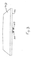
- FIG 3 is a perspective view of a practical embodiment of a four antenna stacked patch antenna assembly 300, such as illustrated in simplified view in Figure 1.
- Figure 4 is a cross-sectional side view of the same antenna assembly.
- the antenna assembly components as discussed above in connection with Figure 1, for example, are contained within a housing comprising a conducting base 301 and a radome 303.
- the conductive base 301 nests within the bottom of the radome 303.
- Protruding from the base are two coaxial connectors 305, 307 that provide a feedthrough connection to the patch antennas (see Figure 4). Signals are passed between each antenna and transmitting circuitry external of the antenna (not shown) through coaxial cables (also not shown) coupled to coaxial connectors 305 and 307.
- the circuit board 301 serves as the ground plane for the patch antennas 403, 405, 407. 409.
- the central coaxial feed 411 for the two uppermost antennas 403, 405 is constructed from a coaxial cable.
- An inner conductor 411a extends from the electrical connector 305 to the conductive basket 416.
- the upper end of the inner conductor 411a is terminated in the conductive basket 416, which resiliently grips the inner conductor to establish an electrical connection with radiating patch 403a of patch antenna 403.
- the basket 416 comprises an electrical receptacle with spring fingers that grip the inner conductor 411a.
- the basket 416 is electrically connected to the radiating patch 403a by, for example, a solder joint.
- the lower end of the inner conductor 411a comprises an electrical receptacle with spring fingers that grip the inner conductor 305a of the electrical connector 305 to form an electrical connection.
- the outer conductor 411c extends from the ground plane through antennas 407, 409. The outer conductor is electrically connected to the base 301 by, for example, a solder joint.
- the outer conductor is coupled to the two lower patch antennas 407, 409 by conducting flanged sleeve 413 (shown here only for antenna 407 for clarity).
- the outer conductor is electrically connected to the sleeves 413 by, for example, a solder joint.
- the sleeve 413 is electrically connected to the radiating patches 407a, 409a by, for example, a solder joint.
- a dielectric sleeve 411b is concentric with, and extends between, inner conductor 411a and outer conductor 411c.
- a second coaxial feed 415 for the two lowermost antennas 407, 409 is constructed as a coaxial cable.
- An inner conductor 415a extends from the electrical connector 307 to a conductive basket 420.
- the upper end of the inner conductor 415a is terminated in the conductive basket 420 that resiliently grips the inner conductor 415a to establish an electrical connection with radiating patch 407a of patch antenna 407.
- the basket 420 comprises an electrical receptacle with spring fingers that grip the inner conductor 415a.
- the basket 420 is electrically connected to the radiating patch 407a by, for example, a solder joint.
- the lower end of the inner conductor 415a comprises an electrical receptacle with spring fingers that grip the inner conductor 307a of the electrical connector 307 to form an electrical connection.
- the outer conductor 415c is electrically connected to the base 301 by, for example, a solder joint.
- a dielectric sleeve 415b is concentric with and extends between inner conductor 415a and outer conductor 415c.
- a stacked patch antenna assembly comprising four antennas in accordance with the present invention was constructed to determine the isolation parameters and other parameters of the invention.
- the prototype was arbitrarily designed to produce omni-directional radiation patterns for the two highest frequencies.
- the uppermost layer was a 2400 MHZ antenna with a square radiating patch 17.5mm (0.690) inches per side on a 5.1mm (0.2 inch) substrate.
- the feed point was at the geometric center of the patch.
- the second uppermost patch antenna was designed to resonate at 1900 MHZ and had a square radiating patch 19.8mm (0.780 inches) per side on a 4.6mm (0.18 inch) thick substrate.
- a 3.8mm (0.150 inch) diameter circle was removed from the center of the radiating patch to accommodate the central conductor of the feed line for the upper antennas.
- the third uppermost (which is the second lowermost) patch antenna was designed to resonate at 1575 MHZ and had a square radiating patch 23.4mm (0.922 inches) per side on a 4.6mm (0.18 inch) thick substrate. The feed point was located 7.1mm (0.280) inches from the patch center line.
- the lowermost antenna was designed to resonate at 1227 MHZ and had a square radiating patch 34.5mm (1.36 inches) per side on a 4.6mm (0.18 inch) thick substrate. It had a 3.8mm (0.150 inch) diameter circular aperture at its center to accommodate the inner and outer conductors of the central coaxial cable. Only this lowermost antenna had a ground metalization on the bottom of the dielectric substrate of the antenna.
- the outer conductor of a 2.2mm (0.085 inch) coaxial cable feeding the uppermost two patch antennas was electrically connected to the center of both of the two lower patch antennas as well as to the ground plane.
- the outer conductor of the 1575 MHZ antenna feed was electrically connected to the ground plane.
- the stacked patch antenna assembly was mounted on a 46mm (18 inch) diameter ground plane for testing. Measured impedance results for the GPS bands are shown in Figure 5. The measured resonance for the L2 band is higher in frequency than nominal by about 10% and the L1 band is higher by about approximately 5%. However, both of these patches were fabricated approximately 5% over-sized to allow for tuning. Accordingly, these results are in excellent agreement with expectations. In both cases, the measured 2:1 VSWR (Voltage Standing Wave Ratio) bandwidth (approximately 40 MHZ) is somewhat larger than predicted and adequate for the application.
- VSWR Voltage Standing Wave Ratio
- Figures 6A and 6B show the measured radiation pattern for the L2 GPS antenna (1350 MHZ) for ⁇ of 0° and 90°, respectively, and are representative of normal mode patterns.
- the L1 patterns are similar with slightly smaller beam width. Both are in good agreement with predicted results.
- Figures 8A and 8B are measured radiation patterns from the 2400 MHZ antenna (the uppermost antenna) for ⁇ of 0° and 90°, respectively. Although the gain is low due to the impedance mismatch, the desired omni-directional pattern is radiated, again confirming expected results. Radiation patterns at 1900 MHZ are similar, although there is some asymmetry and the gain is lower than at 2400 MHZ.
- Isolation between the two GPS bands, on the one hand, and the cellular communication bands, on the other hand, is better than 20dB, as illustrated in Figure 9, which is a plot of insertion loss between the two coaxial ports as a function of frequency.
- inductive posts were added at the edges of the uppermost patch. The posts were shorted to both the 2400 MHZ patch and the 1900 MHZ patch. Model results are shown in Figure 10 and indicate improved impedance matching.
Applications Claiming Priority (2)
| Application Number | Priority Date | Filing Date | Title |
|---|---|---|---|
| US68032 | 2002-02-06 | ||
| US10/068,032 US6639558B2 (en) | 2002-02-06 | 2002-02-06 | Multi frequency stacked patch antenna with improved frequency band isolation |
Publications (2)
| Publication Number | Publication Date |
|---|---|
| EP1341259A1 true EP1341259A1 (de) | 2003-09-03 |
| EP1341259B1 EP1341259B1 (de) | 2005-07-27 |
Family
ID=27658948
Family Applications (1)
| Application Number | Title | Priority Date | Filing Date |
|---|---|---|---|
| EP03250716A Expired - Fee Related EP1341259B1 (de) | 2002-02-06 | 2003-02-05 | Geschichtete Streifenleitungsantenne für mehrere Frequenzen mit verbesserter Frequenzbandisolation |
Country Status (4)
| Country | Link |
|---|---|
| US (1) | US6639558B2 (de) |
| EP (1) | EP1341259B1 (de) |
| JP (1) | JP4097258B2 (de) |
| DE (1) | DE60301077T2 (de) |
Cited By (3)
| Publication number | Priority date | Publication date | Assignee | Title |
|---|---|---|---|---|
| WO2010035934A3 (en) * | 2008-09-23 | 2010-05-27 | Electronics And Telecommunications Research Institute | Conductive structure for high gain antenna and antenna |
| CN105359339A (zh) * | 2013-08-07 | 2016-02-24 | 华为技术有限公司 | 宽带低波束耦合双波束相控阵列 |
| CN110462929A (zh) * | 2017-03-14 | 2019-11-15 | 阿莫技术有限公司 | 多层贴片天线 |
Families Citing this family (110)
| Publication number | Priority date | Publication date | Assignee | Title |
|---|---|---|---|---|
| DE10064128A1 (de) * | 2000-12-21 | 2002-07-25 | Kathrein Werke Kg | Patch-Antenne für den Betrieb in mindestens zwei Frequenzbereichen |
| US6456243B1 (en) * | 2001-06-26 | 2002-09-24 | Ethertronics, Inc. | Multi frequency magnetic dipole antenna structures and methods of reusing the volume of an antenna |
| JP2003283240A (ja) * | 2002-03-25 | 2003-10-03 | Yazaki Corp | 多周波共振積層パッチアンテナ |
| EP1353405A1 (de) * | 2002-04-10 | 2003-10-15 | Huber & Suhner Ag | Dualbandantenne |
| US6870505B2 (en) * | 2002-07-01 | 2005-03-22 | Integral Technologies, Inc. | Multi-segmented planar antenna with built-in ground plane |
| US6950066B2 (en) * | 2002-08-22 | 2005-09-27 | Skycross, Inc. | Apparatus and method for forming a monolithic surface-mountable antenna |
| US6812891B2 (en) * | 2002-11-07 | 2004-11-02 | Skycross, Inc. | Tri-band multi-mode antenna |
| US20040110481A1 (en) * | 2002-12-07 | 2004-06-10 | Umesh Navsariwala | Antenna and wireless device utilizing the antenna |
| US6975267B2 (en) * | 2003-02-05 | 2005-12-13 | Northrop Grumman Corporation | Low profile active electronically scanned antenna (AESA) for Ka-band radar systems |
| TW578333B (en) * | 2003-02-18 | 2004-03-01 | Gemtek Technology Co Ltd | Dual-frequency antenna |
| US6903687B1 (en) * | 2003-05-29 | 2005-06-07 | The United States Of America As Represented By The United States National Aeronautics And Space Administration | Feed structure for antennas |
| TW584978B (en) * | 2003-07-10 | 2004-04-21 | Quanta Comp Inc | Grounding module of antenna in portable electronic device |
| JP2005236393A (ja) * | 2004-02-17 | 2005-09-02 | Alps Electric Co Ltd | 異周波共用アンテナ |
| US7084815B2 (en) * | 2004-03-22 | 2006-08-01 | Motorola, Inc. | Differential-fed stacked patch antenna |
| US20060001574A1 (en) * | 2004-07-03 | 2006-01-05 | Think Wireless, Inc. | Wideband Patch Antenna |
| DE102004035064A1 (de) * | 2004-07-20 | 2006-02-16 | Receptec Gmbh | Antennenmodul |
| US20060092078A1 (en) * | 2004-11-02 | 2006-05-04 | Calamp Corporate | Antenna systems for widely-spaced frequency bands of wireless communication networks |
| SE528084C2 (sv) * | 2004-11-30 | 2006-08-29 | Powerwave Technologies Sweden | Matning för dubbelbandantenn |
| US7525489B2 (en) * | 2004-12-07 | 2009-04-28 | Sony Ericsson Mobile Communications Ab | Digital video broadcast-handheld (DVB-H) antennas for wireless terminals |
| US7038625B1 (en) * | 2005-01-14 | 2006-05-02 | Harris Corporation | Array antenna including a monolithic antenna feed assembly and related methods |
| WO2006086658A1 (en) * | 2005-02-11 | 2006-08-17 | Cornwell, James | Antenna system |
| US7385561B2 (en) * | 2005-02-17 | 2008-06-10 | Galtronics Ltd. | Multiple monopole antenna |
| US20060220962A1 (en) * | 2005-02-28 | 2006-10-05 | D Hont Loek J | Circularly polorized square patch antenna |
| US7696927B2 (en) * | 2005-03-15 | 2010-04-13 | Galtronics Ltd. | Capacitive feed antenna |
| US20060232475A1 (en) * | 2005-04-15 | 2006-10-19 | Cirex Technology Corporation | Dual-band strip antenna supporting left-hand and right-hand circular polarization |
| US20070026898A1 (en) * | 2005-07-26 | 2007-02-01 | Lear Corporation | System and method for use in wireless communication employing multiple antennas |
| US20070026897A1 (en) * | 2005-07-26 | 2007-02-01 | Lear Corporation | System and method for use in wireless communication employing antenna network |
| US20070024510A1 (en) * | 2005-07-26 | 2007-02-01 | Lear Corporation | System and method for use in wireless communication employing multiple antennas |
| WO2007132262A1 (en) * | 2006-05-11 | 2007-11-22 | Bae Systems Plc | Stacked multiband antenna |
| EP2025043A2 (de) * | 2006-06-08 | 2009-02-18 | Fractus, S.A. | Gegenüber menschenkörper-lasteffekten robustes verteiltes antennensystem |
| DE102006038528B3 (de) * | 2006-08-17 | 2007-11-22 | Kathrein-Werke Kg | Abstimmbare Antenne planarer Bauart |
| US8111196B2 (en) * | 2006-09-15 | 2012-02-07 | Laird Technologies, Inc. | Stacked patch antennas |
| US7277056B1 (en) * | 2006-09-15 | 2007-10-02 | Laird Technologies, Inc. | Stacked patch antennas |
| US7492319B2 (en) * | 2006-09-22 | 2009-02-17 | Laird Technologies, Inc. | Antenna assemblies including standard electrical connections and captured retainers and fasteners |
| CN103199343B (zh) * | 2006-11-06 | 2016-08-10 | 株式会社村田制作所 | 贴片天线装置和天线装置 |
| US7498989B1 (en) * | 2007-04-26 | 2009-03-03 | Lockheed Martin Corporation | Stacked-disk antenna element with wings, and array thereof |
| DE112008001621T5 (de) * | 2007-06-14 | 2010-04-22 | Kyocera Corp. | Gleichstromsperrschaltung, Hybridschaltungsvorrichtung, Sender, Empfänger, Sender-Empfänger und Radarvorrichtung |
| US7916089B2 (en) * | 2008-01-04 | 2011-03-29 | Apple Inc. | Antenna isolation for portable electronic devices |
| US8022861B2 (en) | 2008-04-04 | 2011-09-20 | Toyota Motor Engineering & Manufacturing North America, Inc. | Dual-band antenna array and RF front-end for mm-wave imager and radar |
| US7733265B2 (en) * | 2008-04-04 | 2010-06-08 | Toyota Motor Engineering & Manufacturing North America, Inc. | Three dimensional integrated automotive radars and methods of manufacturing the same |
| US7830301B2 (en) | 2008-04-04 | 2010-11-09 | Toyota Motor Engineering & Manufacturing North America, Inc. | Dual-band antenna array and RF front-end for automotive radars |
| US7800542B2 (en) * | 2008-05-23 | 2010-09-21 | Agc Automotive Americas R&D, Inc. | Multi-layer offset patch antenna |
| US7990237B2 (en) * | 2009-01-16 | 2011-08-02 | Toyota Motor Engineering & Manufacturing North America, Inc. | System and method for improving performance of coplanar waveguide bends at mm-wave frequencies |
| FR2946806B1 (fr) | 2009-06-11 | 2012-03-30 | Alcatel Lucent | Element rayonnant d'antenne multi-bande |
| TWI381585B (zh) * | 2009-06-30 | 2013-01-01 | Wistron Neweb Corp | 雙頻天線裝置 |
| US8633856B2 (en) * | 2009-07-02 | 2014-01-21 | Blackberry Limited | Compact single feed dual-polarized dual-frequency band microstrip antenna array |
| US8325093B2 (en) * | 2009-07-31 | 2012-12-04 | University Of Massachusetts | Planar ultrawideband modular antenna array |
| US8228238B2 (en) * | 2009-10-02 | 2012-07-24 | Laird Technologies, Inc. | Low profile antenna assemblies |
| EP2502311B1 (de) * | 2009-11-17 | 2017-02-01 | Topcon Positioning Systems, Inc. | Kompaktes mehrwegeresistentes antennensystem mit integriertem navigationsempfänger |
| US8754819B2 (en) * | 2010-03-12 | 2014-06-17 | Agc Automotive Americas R&D, Inc. | Antenna system including a circularly polarized antenna |
| TWM393051U (en) * | 2010-06-09 | 2010-11-21 | Cameo Communications Inc | Dual band antenna and wireless network device with the aforementioned dual band antenna |
| US8786496B2 (en) | 2010-07-28 | 2014-07-22 | Toyota Motor Engineering & Manufacturing North America, Inc. | Three-dimensional array antenna on a substrate with enhanced backlobe suppression for mm-wave automotive applications |
| US9236648B2 (en) | 2010-09-22 | 2016-01-12 | Apple Inc. | Antenna structures having resonating elements and parasitic elements within slots in conductive elements |
| US8941539B1 (en) * | 2011-02-23 | 2015-01-27 | Meru Networks | Dual-stack dual-band MIMO antenna |
| US9024831B2 (en) * | 2011-05-26 | 2015-05-05 | Wang-Electro-Opto Corporation | Miniaturized ultra-wideband multifunction antenna via multi-mode traveling-waves (TW) |
| TWM422771U (en) * | 2011-05-27 | 2012-02-11 | Unictron Technologies Corp | Micro antenna and micro antenna device |
| CN102270780B (zh) * | 2011-07-28 | 2014-02-12 | 四川九洲电器集团有限责任公司 | 一种工作于毫米波和l频段的宽频带一体化全向天线 |
| JP5790398B2 (ja) | 2011-10-19 | 2015-10-07 | 富士通株式会社 | パッチアンテナ |
| US20130120213A1 (en) * | 2011-11-11 | 2013-05-16 | Utah State University | Broadband antenna systems and methods |
| KR101952173B1 (ko) * | 2012-01-31 | 2019-02-26 | 엘지전자 주식회사 | 이동 단말기 |
| US9203139B2 (en) | 2012-05-04 | 2015-12-01 | Apple Inc. | Antenna structures having slot-based parasitic elements |
| US9425516B2 (en) | 2012-07-06 | 2016-08-23 | The Ohio State University | Compact dual band GNSS antenna design |
| US10158167B2 (en) * | 2012-07-24 | 2018-12-18 | Novatel Inc. | Irridium/inmarsat and GNSS antenna system |
| US9306266B2 (en) * | 2012-09-21 | 2016-04-05 | Aalto University Foundation | Multi-band antenna for wireless communication |
| CN102882013A (zh) * | 2012-09-26 | 2013-01-16 | 华为技术有限公司 | 低剖面宽频带天线阵子和天线 |
| CN102904071A (zh) * | 2012-09-29 | 2013-01-30 | 西安空间无线电技术研究所 | 一种l波段三频圆极化微带天线 |
| KR101870760B1 (ko) * | 2012-11-08 | 2018-06-25 | 삼성전자주식회사 | 다중 대역 안테나 장치 및 이를 구비하는 전자기기 |
| JP6051879B2 (ja) | 2013-01-11 | 2016-12-27 | 富士通株式会社 | パッチアンテナ |
| KR102116159B1 (ko) * | 2013-04-01 | 2020-05-28 | 에이브이엑스 안테나 인코포레이티드 | 재구성 가능 다중 모드 능동 안테나 시스템 |
| US9680202B2 (en) | 2013-06-05 | 2017-06-13 | Apple Inc. | Electronic devices with antenna windows on opposing housing surfaces |
| CN103441332B (zh) * | 2013-08-21 | 2016-12-28 | 华为技术有限公司 | 一种微带阵列天线及基站 |
| CN103531902B (zh) * | 2013-10-24 | 2015-09-30 | 哈尔滨工程大学 | 可降互耦探针与贴片相切馈电方式天线 |
| CN103531891B (zh) * | 2013-10-24 | 2015-07-22 | 哈尔滨工程大学 | 宽带高增益探针与贴片相切层叠微带天线 |
| US9450289B2 (en) | 2014-03-10 | 2016-09-20 | Apple Inc. | Electronic device with dual clutch barrel cavity antennas |
| WO2016032355A1 (en) * | 2014-08-26 | 2016-03-03 | Limited Liability Company "Topcon Positioning Systems" | Antenna system with reduced multipath reception |
| US10193231B2 (en) * | 2015-03-02 | 2019-01-29 | Trimble Inc. | Dual-frequency patch antennas |
| US9653777B2 (en) | 2015-03-06 | 2017-05-16 | Apple Inc. | Electronic device with isolated cavity antennas |
| KR102117473B1 (ko) * | 2015-03-18 | 2020-06-01 | 삼성전기주식회사 | 실장 기판 모듈, 안테나 장치 및 실장 기판 모듈 제조 방법 |
| US9666943B2 (en) | 2015-08-05 | 2017-05-30 | Matsing Inc. | Lens based antenna for super high capacity wireless communications systems |
| US9941595B2 (en) * | 2015-08-12 | 2018-04-10 | Novatel Inc. | Patch antenna with peripheral parasitic monopole circular arrays |
| US10205240B2 (en) | 2015-09-30 | 2019-02-12 | The Mitre Corporation | Shorted annular patch antenna with shunted stubs |
| US9991601B2 (en) * | 2015-09-30 | 2018-06-05 | The Mitre Corporation | Coplanar waveguide transition for multi-band impedance matching |
| US11303026B2 (en) * | 2015-12-09 | 2022-04-12 | Viasat, Inc. | Stacked self-diplexed dual-band patch antenna |
| US10268236B2 (en) | 2016-01-27 | 2019-04-23 | Apple Inc. | Electronic devices having ventilation systems with antennas |
| CN105932419A (zh) * | 2016-07-01 | 2016-09-07 | 西安电子科技大学 | 基于阶梯型层叠结构的多频段封装天线 |
| JP6833523B2 (ja) * | 2017-01-11 | 2021-02-24 | 株式会社デンソーテン | マイクロストリップアンテナ |
| JP6855258B2 (ja) * | 2017-01-24 | 2021-04-07 | 原田工業株式会社 | 複合アンテナ装置 |
| CN106785455B (zh) * | 2017-03-14 | 2022-05-13 | 昆山瀚德通信科技有限公司 | 超宽带壁挂天线 |
| TWI689130B (zh) * | 2017-08-02 | 2020-03-21 | 佳邦科技股份有限公司 | 可攜式電子裝置及其堆疊式天線模組 |
| JP6723470B2 (ja) * | 2017-09-29 | 2020-07-15 | 三菱電機株式会社 | アンテナ装置 |
| CN111095675A (zh) * | 2017-10-03 | 2020-05-01 | 英特尔公司 | 混合且薄化的毫米波天线解决方案 |
| US10693235B2 (en) * | 2018-01-12 | 2020-06-23 | The Government Of The United States, As Represented By The Secretary Of The Army | Patch antenna elements and parasitic feed pads |
| TWI678784B (zh) | 2018-03-01 | 2019-12-01 | 矽品精密工業股份有限公司 | 電子封裝件及其製法 |
| US20220231410A1 (en) * | 2018-07-15 | 2022-07-21 | Shenzhen Merrytek Technology Co., Ltd. | Anti-Interference Microwave Antenna |
| US10784593B1 (en) | 2018-08-02 | 2020-09-22 | United States Of America As Represented By The Administrator Of The National Aeronautics And Space Administration | Dual-band and wideband patch antenna |
| KR102566993B1 (ko) | 2018-10-24 | 2023-08-14 | 삼성전자주식회사 | 안테나 모듈 및 이를 포함하는 rf 장치 |
| KR102166126B1 (ko) * | 2019-04-11 | 2020-10-15 | 삼성전기주식회사 | 칩 안테나 모듈 및 이를 포함하는 전자기기 |
| US11158948B2 (en) * | 2019-03-20 | 2021-10-26 | Samsung Electro-Mechanics Co., Ltd. | Antenna apparatus |
| CN112400255B (zh) * | 2019-04-24 | 2023-06-27 | 株式会社村田制作所 | 天线模块和搭载有该天线模块的通信装置 |
| JP6917419B2 (ja) * | 2019-08-02 | 2021-08-11 | 原田工業株式会社 | 積層型パッチアンテナ |
| FR3101486B1 (fr) * | 2019-09-27 | 2021-09-24 | Office National Detudes Rech Aerospatiales | Antenne multi-bande |
| CN112582787B (zh) | 2019-09-30 | 2022-04-22 | 华为技术有限公司 | 一种天线结构和电子设备 |
| SG10201909947YA (en) | 2019-10-24 | 2021-05-28 | Pci Private Ltd | Antenna system |
| CN112751178A (zh) * | 2019-10-29 | 2021-05-04 | 北京小米移动软件有限公司 | 天线单元、阵列天线及电子设备 |
| CN111009726A (zh) * | 2019-12-31 | 2020-04-14 | 上海海积信息科技股份有限公司 | 一种多频段天线 |
| US11502414B2 (en) * | 2021-01-29 | 2022-11-15 | Eagle Technology, Llc | Microstrip patch antenna system having adjustable radiation pattern shapes and related method |
| KR20230011050A (ko) * | 2021-07-13 | 2023-01-20 | 삼성전기주식회사 | 안테나 장치 |
| WO2023089207A1 (es) | 2021-11-17 | 2023-05-25 | Airbus Defence And Space, S.A. | Antena de parches apilados |
| US20230253715A1 (en) * | 2021-12-27 | 2023-08-10 | Electronic Design & Development, Corp. | Dual-polarized antennas |
| DE102022200018A1 (de) | 2022-01-04 | 2023-07-06 | Continental Automotive Technologies GmbH | Mehrschichtige Patchantennenvorrichtung und Fahrzeug |
Citations (6)
| Publication number | Priority date | Publication date | Assignee | Title |
|---|---|---|---|---|
| US4131893A (en) * | 1977-04-01 | 1978-12-26 | Ball Corporation | Microstrip radiator with folded resonant cavity |
| US4218682A (en) * | 1979-06-22 | 1980-08-19 | Nasa | Multiple band circularly polarized microstrip antenna |
| EP0362079A2 (de) * | 1988-09-30 | 1990-04-04 | Sony Corporation | Mikrostreifenantenne |
| EP0521384A1 (de) * | 1991-07-01 | 1993-01-07 | Ball Corporation | Schichtartig aufgebaute Mehrfachfrequenz-Streifenleiterantenne |
| EP0871238A2 (de) * | 1997-03-25 | 1998-10-14 | Nokia Mobile Phones Ltd. | Breitbandige Antenne mit kurzgeschlossenen Mikrostreifenleitern |
| WO1998049748A1 (en) * | 1997-04-29 | 1998-11-05 | The Whitaker Corporation | Stacked patch antenna with frequency band isolation |
Family Cites Families (2)
| Publication number | Priority date | Publication date | Assignee | Title |
|---|---|---|---|---|
| US5307075A (en) * | 1991-12-12 | 1994-04-26 | Allen Telecom Group, Inc. | Directional microstrip antenna with stacked planar elements |
| US6118406A (en) * | 1998-12-21 | 2000-09-12 | The United States Of America As Represented By The Secretary Of The Navy | Broadband direct fed phased array antenna comprising stacked patches |
-
2002
- 2002-02-06 US US10/068,032 patent/US6639558B2/en not_active Expired - Fee Related
-
2003
- 2003-02-05 DE DE60301077T patent/DE60301077T2/de not_active Expired - Lifetime
- 2003-02-05 EP EP03250716A patent/EP1341259B1/de not_active Expired - Fee Related
- 2003-02-06 JP JP2003029860A patent/JP4097258B2/ja not_active Expired - Fee Related
Patent Citations (6)
| Publication number | Priority date | Publication date | Assignee | Title |
|---|---|---|---|---|
| US4131893A (en) * | 1977-04-01 | 1978-12-26 | Ball Corporation | Microstrip radiator with folded resonant cavity |
| US4218682A (en) * | 1979-06-22 | 1980-08-19 | Nasa | Multiple band circularly polarized microstrip antenna |
| EP0362079A2 (de) * | 1988-09-30 | 1990-04-04 | Sony Corporation | Mikrostreifenantenne |
| EP0521384A1 (de) * | 1991-07-01 | 1993-01-07 | Ball Corporation | Schichtartig aufgebaute Mehrfachfrequenz-Streifenleiterantenne |
| EP0871238A2 (de) * | 1997-03-25 | 1998-10-14 | Nokia Mobile Phones Ltd. | Breitbandige Antenne mit kurzgeschlossenen Mikrostreifenleitern |
| WO1998049748A1 (en) * | 1997-04-29 | 1998-11-05 | The Whitaker Corporation | Stacked patch antenna with frequency band isolation |
Non-Patent Citations (1)
| Title |
|---|
| SANAD M ET AL: "A COMPACT DUAL-BAND MICROSTRIP ANTENNA FOR PORTABLE GPS/CELLULAR PHONES", IEEE ANTENNAS AND PROPAGATION SOCIETY INTERNATIONAL SYMPOSIUM. 1999 DIGEST. APS. ORLANDO, FL, JULY 11 - 16, 1999, NEW YORK, NY: IEEE, US, vol. 1, 11 July 1999 (1999-07-11), pages 116 - 119, XP000927428, ISBN: 0-7803-5640-3 * |
Cited By (6)
| Publication number | Priority date | Publication date | Assignee | Title |
|---|---|---|---|---|
| WO2010035934A3 (en) * | 2008-09-23 | 2010-05-27 | Electronics And Telecommunications Research Institute | Conductive structure for high gain antenna and antenna |
| CN105359339A (zh) * | 2013-08-07 | 2016-02-24 | 华为技术有限公司 | 宽带低波束耦合双波束相控阵列 |
| US9711853B2 (en) | 2013-08-07 | 2017-07-18 | Huawei Technologies Co., Ltd. | Broadband low-beam-coupling dual-beam phased array |
| CN105359339B (zh) * | 2013-08-07 | 2018-03-09 | 华为技术有限公司 | 宽带低波束耦合双波束相控阵列 |
| US10804606B2 (en) | 2013-08-07 | 2020-10-13 | Huawei Technologies Co., Ltd. | Broadband low-beam-coupling dual-beam phased array |
| CN110462929A (zh) * | 2017-03-14 | 2019-11-15 | 阿莫技术有限公司 | 多层贴片天线 |
Also Published As
| Publication number | Publication date |
|---|---|
| DE60301077D1 (de) | 2005-09-01 |
| JP4097258B2 (ja) | 2008-06-11 |
| JP2003258540A (ja) | 2003-09-12 |
| EP1341259B1 (de) | 2005-07-27 |
| DE60301077T2 (de) | 2006-05-24 |
| US6639558B2 (en) | 2003-10-28 |
| US20030146872A1 (en) | 2003-08-07 |
Similar Documents
| Publication | Publication Date | Title |
|---|---|---|
| EP1341259B1 (de) | Geschichtete Streifenleitungsantenne für mehrere Frequenzen mit verbesserter Frequenzbandisolation | |
| EP0449492B1 (de) | Streifenleitungsantenne mit gesicherter Gleichmässigkeit der Polarisation | |
| EP0720252B1 (de) | Miniatur-Streifenleitungsantenne mit mehreren Zweigen | |
| US6424300B1 (en) | Notch antennas and wireless communicators incorporating same | |
| US4827266A (en) | Antenna with lumped reactive matching elements between radiator and groundplate | |
| EP1590857B1 (de) | Doppelfrequenz-dipolantennenstruktur mit niedrigem profil | |
| US6292141B1 (en) | Dielectric-patch resonator antenna | |
| US6529749B1 (en) | Convertible dipole/inverted-F antennas and wireless communicators incorporating the same | |
| US5210542A (en) | Microstrip patch antenna structure | |
| US6421028B1 (en) | Dual frequency quadrifilar helix antenna | |
| US5444452A (en) | Dual frequency antenna | |
| EP1679763B1 (de) | Antenne | |
| EP0847101A2 (de) | Neutralisation von gegenseitiger Antennenkopplung | |
| US10236578B2 (en) | Antenna structures and associated methods for construction and use | |
| US6466177B1 (en) | Controlled radiation pattern array antenna using spiral slot array elements | |
| WO1993009577A1 (en) | Terrestrial antennas for satellite communication system | |
| US11799207B2 (en) | Antennas for reception of satellite signals | |
| US5940037A (en) | Stacked patch antenna with frequency band isolation | |
| US4940991A (en) | Discontinuous mobile antenna | |
| EP0824766A1 (de) | Antenne | |
| JP2824384B2 (ja) | 2周波共用マイクロストリップアンテナ | |
| JP3006399B2 (ja) | デュアルバンドアンテナ | |
| EP1069646A2 (de) | Streifenleiterantenne |
Legal Events
| Date | Code | Title | Description |
|---|---|---|---|
| PUAI | Public reference made under article 153(3) epc to a published international application that has entered the european phase |
Free format text: ORIGINAL CODE: 0009012 |
|
| AK | Designated contracting states |
Kind code of ref document: A1 Designated state(s): AT BE BG CH CY CZ DE DK EE ES FI FR GB GR HU IE IT LI LU MC NL PT SE SI SK TR |
|
| AX | Request for extension of the european patent |
Extension state: AL LT LV MK RO |
|
| 17P | Request for examination filed |
Effective date: 20040303 |
|
| 17Q | First examination report despatched |
Effective date: 20040406 |
|
| AKX | Designation fees paid |
Designated state(s): DE FI FR GB SE |
|
| GRAP | Despatch of communication of intention to grant a patent |
Free format text: ORIGINAL CODE: EPIDOSNIGR1 |
|
| GRAS | Grant fee paid |
Free format text: ORIGINAL CODE: EPIDOSNIGR3 |
|
| GRAA | (expected) grant |
Free format text: ORIGINAL CODE: 0009210 |
|
| AK | Designated contracting states |
Kind code of ref document: B1 Designated state(s): DE FI FR GB SE |
|
| PG25 | Lapsed in a contracting state [announced via postgrant information from national office to epo] |
Ref country code: FI Free format text: LAPSE BECAUSE OF FAILURE TO SUBMIT A TRANSLATION OF THE DESCRIPTION OR TO PAY THE FEE WITHIN THE PRESCRIBED TIME-LIMIT Effective date: 20050727 |
|
| REG | Reference to a national code |
Ref country code: GB Ref legal event code: FG4D |
|
| REF | Corresponds to: |
Ref document number: 60301077 Country of ref document: DE Date of ref document: 20050901 Kind code of ref document: P |
|
| PG25 | Lapsed in a contracting state [announced via postgrant information from national office to epo] |
Ref country code: SE Free format text: LAPSE BECAUSE OF FAILURE TO SUBMIT A TRANSLATION OF THE DESCRIPTION OR TO PAY THE FEE WITHIN THE PRESCRIBED TIME-LIMIT Effective date: 20051027 |
|
| ET | Fr: translation filed | ||
| PLBE | No opposition filed within time limit |
Free format text: ORIGINAL CODE: 0009261 |
|
| STAA | Information on the status of an ep patent application or granted ep patent |
Free format text: STATUS: NO OPPOSITION FILED WITHIN TIME LIMIT |
|
| 26N | No opposition filed |
Effective date: 20060428 |
|
| REG | Reference to a national code |
Ref country code: GB Ref legal event code: 732E Free format text: REGISTERED BETWEEN 20090514 AND 20090520 |
|
| REG | Reference to a national code |
Ref country code: FR Ref legal event code: TP |
|
| PGFP | Annual fee paid to national office [announced via postgrant information from national office to epo] |
Ref country code: FR Payment date: 20100601 Year of fee payment: 8 |
|
| PGFP | Annual fee paid to national office [announced via postgrant information from national office to epo] |
Ref country code: DE Payment date: 20100527 Year of fee payment: 8 Ref country code: GB Payment date: 20100525 Year of fee payment: 8 |
|
| GBPC | Gb: european patent ceased through non-payment of renewal fee |
Effective date: 20110205 |
|
| REG | Reference to a national code |
Ref country code: FR Ref legal event code: ST Effective date: 20111102 |
|
| REG | Reference to a national code |
Ref country code: DE Ref legal event code: R119 Ref document number: 60301077 Country of ref document: DE Effective date: 20110901 |
|
| PG25 | Lapsed in a contracting state [announced via postgrant information from national office to epo] |
Ref country code: FR Free format text: LAPSE BECAUSE OF NON-PAYMENT OF DUE FEES Effective date: 20110228 |
|
| PG25 | Lapsed in a contracting state [announced via postgrant information from national office to epo] |
Ref country code: GB Free format text: LAPSE BECAUSE OF NON-PAYMENT OF DUE FEES Effective date: 20110205 |
|
| PG25 | Lapsed in a contracting state [announced via postgrant information from national office to epo] |
Ref country code: DE Free format text: LAPSE BECAUSE OF NON-PAYMENT OF DUE FEES Effective date: 20110901 |