EP1335412A2 - Dispositif et procédé de traitement de substrat - Google Patents
Dispositif et procédé de traitement de substrat Download PDFInfo
- Publication number
- EP1335412A2 EP1335412A2 EP03001859A EP03001859A EP1335412A2 EP 1335412 A2 EP1335412 A2 EP 1335412A2 EP 03001859 A EP03001859 A EP 03001859A EP 03001859 A EP03001859 A EP 03001859A EP 1335412 A2 EP1335412 A2 EP 1335412A2
- Authority
- EP
- European Patent Office
- Prior art keywords
- liquid
- pretreatment
- wafer
- substrate
- etching
- Prior art date
- Legal status (The legal status is an assumption and is not a legal conclusion. Google has not performed a legal analysis and makes no representation as to the accuracy of the status listed.)
- Granted
Links
Images


Classifications
-
- H—ELECTRICITY
- H01—ELECTRIC ELEMENTS
- H01L—SEMICONDUCTOR DEVICES NOT COVERED BY CLASS H10
- H01L21/00—Processes or apparatus adapted for the manufacture or treatment of semiconductor or solid state devices or of parts thereof
- H01L21/02—Manufacture or treatment of semiconductor devices or of parts thereof
- H01L21/04—Manufacture or treatment of semiconductor devices or of parts thereof the devices having at least one potential-jump barrier or surface barrier, e.g. PN junction, depletion layer or carrier concentration layer
- H01L21/18—Manufacture or treatment of semiconductor devices or of parts thereof the devices having at least one potential-jump barrier or surface barrier, e.g. PN junction, depletion layer or carrier concentration layer the devices having semiconductor bodies comprising elements of Group IV of the Periodic System or AIIIBV compounds with or without impurities, e.g. doping materials
- H01L21/30—Treatment of semiconductor bodies using processes or apparatus not provided for in groups H01L21/20 - H01L21/26
- H01L21/302—Treatment of semiconductor bodies using processes or apparatus not provided for in groups H01L21/20 - H01L21/26 to change their surface-physical characteristics or shape, e.g. etching, polishing, cutting
- H01L21/304—Mechanical treatment, e.g. grinding, polishing, cutting
-
- H—ELECTRICITY
- H01—ELECTRIC ELEMENTS
- H01L—SEMICONDUCTOR DEVICES NOT COVERED BY CLASS H10
- H01L21/00—Processes or apparatus adapted for the manufacture or treatment of semiconductor or solid state devices or of parts thereof
- H01L21/67—Apparatus specially adapted for handling semiconductor or electric solid state devices during manufacture or treatment thereof; Apparatus specially adapted for handling wafers during manufacture or treatment of semiconductor or electric solid state devices or components ; Apparatus not specifically provided for elsewhere
- H01L21/67005—Apparatus not specifically provided for elsewhere
- H01L21/67011—Apparatus for manufacture or treatment
- H01L21/67017—Apparatus for fluid treatment
- H01L21/67063—Apparatus for fluid treatment for etching
- H01L21/67075—Apparatus for fluid treatment for etching for wet etching
- H01L21/6708—Apparatus for fluid treatment for etching for wet etching using mainly spraying means, e.g. nozzles
-
- B—PERFORMING OPERATIONS; TRANSPORTING
- B05—SPRAYING OR ATOMISING IN GENERAL; APPLYING FLUENT MATERIALS TO SURFACES, IN GENERAL
- B05B—SPRAYING APPARATUS; ATOMISING APPARATUS; NOZZLES
- B05B7/00—Spraying apparatus for discharge of liquids or other fluent materials from two or more sources, e.g. of liquid and air, of powder and gas
- B05B7/02—Spray pistols; Apparatus for discharge
- B05B7/06—Spray pistols; Apparatus for discharge with at least one outlet orifice surrounding another approximately in the same plane
- B05B7/062—Spray pistols; Apparatus for discharge with at least one outlet orifice surrounding another approximately in the same plane with only one liquid outlet and at least one gas outlet
- B05B7/066—Spray pistols; Apparatus for discharge with at least one outlet orifice surrounding another approximately in the same plane with only one liquid outlet and at least one gas outlet with an inner liquid outlet surrounded by at least one annular gas outlet
-
- H—ELECTRICITY
- H01—ELECTRIC ELEMENTS
- H01L—SEMICONDUCTOR DEVICES NOT COVERED BY CLASS H10
- H01L21/00—Processes or apparatus adapted for the manufacture or treatment of semiconductor or solid state devices or of parts thereof
- H01L21/67—Apparatus specially adapted for handling semiconductor or electric solid state devices during manufacture or treatment thereof; Apparatus specially adapted for handling wafers during manufacture or treatment of semiconductor or electric solid state devices or components ; Apparatus not specifically provided for elsewhere
- H01L21/67005—Apparatus not specifically provided for elsewhere
- H01L21/67011—Apparatus for manufacture or treatment
- H01L21/67017—Apparatus for fluid treatment
- H01L21/67028—Apparatus for fluid treatment for cleaning followed by drying, rinsing, stripping, blasting or the like
- H01L21/6704—Apparatus for fluid treatment for cleaning followed by drying, rinsing, stripping, blasting or the like for wet cleaning or washing
- H01L21/67051—Apparatus for fluid treatment for cleaning followed by drying, rinsing, stripping, blasting or the like for wet cleaning or washing using mainly spraying means, e.g. nozzles
Definitions
- the present invention relates to a substrate treatment apparatus and a substrate treatment method for cleaning a surface of a substrate such as a semiconductor substrate.
- Wafer cleaning methods include : a multiple-wafer batch process in which a multiplicity of wafers are immersed in a cleaning liquid at a time; and a wafer-by-wafer process in which wafers are treated on a wafer-by-wafer basis by supplying a cleaning liquid onto a surface of a single wafer while rotating the wafer.
- the wafer-by-wafer cleaning process is disadvantageous in that more time is required for cleaning a single wafer as compared with the multiple-wafer batch cleaning process, but has a process advantage.
- Japanese Unexamined Patent Publication No. HEI10-256211 discloses a cleaning method which employs ozone water and dilute hydrofluoric acid as cleaning liquids.
- ozone water is supplied onto a wafer surface, whereby the wafer surface is oxidized.
- dilute hydrofluoric acid is supplied onto the wafer surface, whereby the resulting oxide layer on the wafer surface is selectively etched away.
- metal contaminants (deposited metals) adhering on the wafer surface are removed together with the oxide layer. Since the layer which bears the particles on the wafer surface is removed, the particles are also removed (lifted off).
- the aforesaid prior-art technique presents a problem such that a greater amount of the wafer surface is etched away (e.g., an etch thickness is 20 ⁇ ). That is, the wafer surface should be etched to a greater thickness for the removal of the particles and the deposited metals in the aforesaid method.
- a substrate treatment apparatus comprises: a pretreatment section for bombarding liquid droplets against a surface of a substrate, the liquid droplets being generated by mixing a pretreatment liquid comprising ammonia and an oxidizing agent with a gas; and an etching liquid supplying section for supplying an etching liquid onto the substrate surface.
- particles adhering on the substrate surface can physically be removed by a kinetic energy of the droplets of the pretreatment liquid bombarded against the substrate.
- the particles once removed from the substrate surface are chemically prevented from adhering again onto the substrate by a repulsive force due to a ⁇ potential.
- the pretreatment liquid is supplied in a liquid droplet form, so that the substrate per se is not subjected to an excessively great force. Even if the substrate to be treated is, for example, a semiconductor substrate having a pattern formed on its surface, there is no possibility that the pattern is damaged. Further, the removal of the particles can be achieved in a shorter time by this physical and chemical method.
- the pretreatment liquid containing ammonia copper (Cu) deposited as a metal deposit on the substrate surface can be dissolved in the form of an ammine complex.
- Ammonia may be present as aqueous ammonia (NH 4 OH) in the pretreatment liquid.
- the pretreatment liquid may be adapted to pretreat the substrate surface into a state suitable for the etching prior to the etching.
- the substrate is a semiconductor substrate such as a silicon substrate, for example, the substrate surface can be oxidized by employing the solution mixture including ammonia and the oxidizing agent as the pretreatment liquid.
- the substrate surface can properly be etched for removal of deposited metals and the like with the use of the etching liquid capable of selectively dissolving the resulting oxide layer on the surface of the semiconductor substrate.
- the particles are already removed, so that it is merely necessary to etch the substrate surface to a smaller thickness. Therefore, the substrate etch amount can be reduced.
- the substrate treatment apparatus may further comprise a substrate holding/rotating mechanism for holding and rotating the substrate. By rotating the substrate, the pretreatment process and the etching process can uniformly be performed on the substrate surface.
- the substrate treatment apparatus may further comprise a pure water supplying mechanism for supplying pure water onto the substrate. In this case, the substrate surface can be rinsed with the pure water supplied thereto after the etching process and between the pretreatment process and the etching process.
- the oxidizing agent may be, for example, hydrogen peroxide.
- the solution mixture as the pretreatment liquid may further comprise water.
- the substrate is a semiconductor substrate such as a silicon substrate, for example, the substrate surface can be oxidized with the use of the pretreatment liquid having such a composition. Thereafter, the resulting oxide layer on the substrate surface is etched away with the etching liquid, whereby the deposited metals can advantageously be removed. That is, the substrate surface can be pretreated into a state suitable for the etching with the use of the pretreatment liquid prior to the etching.
- Solution mixtures containing aqueous ammonia, hydrogen peroxide (H 2 O 2 ) and water (H 2 O) in a wide range of ratios are effective as the pretreatment liquid, but the mixing ratios are preferably 0.05 to 1 part by volume of the aqueous ammonia, 0.1 to 1 part by volume of hydrogen peroxide, and 5 parts by volume of water.
- the oxidizing agent may be ozone water.
- the substrate is a semiconductor substrate such as a silicon substrate, for example, the substrate surface can be oxidized with the use of the pretreatment liquid having such a composition. Thereafter, the resulting oxide layer on the substrate surface is etched away with the use of the etching liquid, whereby the deposited metals can advantageously be removed.
- Solution mixtures containing aqueous ammonia and the ozone water in a wide range of ratios are effective as the pretreatment liquid, but the mixing ratios are preferably 5 to 50 parts by volume of ozone water having an ozone concentration of 5 to 30 ppm, and 1 part by volume of aqueous ammonia.
- the concentrations of the chemical components in the pretreatment liquid may properly be determined depending on the temperature of the pretreatment liquid when it is used. More specifically, the concentrations may be set lower when the pretreatment liquid is used at a higher temperature (e.g., 50 to 80°C), and set higher when the pretreatment is used at a lower temperature (e.g., around an ordinary temperature).
- pretreatment liquid containing aqueous ammonia and hydrogen peroxide as the chemical components is used at an ordinary temperature (20 to 28° C)
- the mixing volume ratio of aqueous ammonia, hydrogen peroxide and water may be about 1:1:5.
- concentrations of aqueous ammonia and hydrogen peroxide may be set lower.
- pretreatment liquid having such a composition
- the surface of the semiconductor substrate can advantageously be oxidized, and the repulsive force due to the ⁇ potential can advantageously be provided. Therefore, the deposited metals can highly effectively be removed during the etching. Since the pretreatment process can be performed in a short time (several tens seconds), the amount of the substrate etched by the pretreatment liquid is negligible.
- the pretreatment section preferably comprises a bi-fluid nozzle including a pretreatment liquid ejecting section for ejecting the pretreatment liquid, and a gas ejecting section provided adjacent the pretreatment liquid ejecting section for ejecting a gas, the bi-fluid nozzle being capable of blowing the gas ejected from the gas ejecting section on the pretreatment liquid ejected from the pretreatment liquid ejecting section for the generation of the droplets of the pretreatment liquid and ejecting the liquid droplets onto the substrate surface.
- the pretreatment liquid can be disintegrated into minute liquid droplets by ejecting the pretreatment liquid from the pretreatment liquid ejecting section, ejecting a high pressure gas (compressed air or an inert gas such as nitrogen (N 2 ) gas) from the gas ejecting section, and blowing the high-pressure gas laterally on the ejected pretreatment liquid.
- a high pressure gas compressed air or an inert gas such as nitrogen (N 2 ) gas
- the size of the droplets of the pretreatment liquid and the bombardment speed against the substrate can be controlled by adjusting the pressure of the high pressure gas.
- the bi-fluid nozzle may be such that the liquid droplets are generated by blowing the gas on the liquid in an open space (external mixing), or such that the liquid droplets are generated by blowing the gas on the liquid in an ejection nozzle and ejected from the ejection nozzle (internal mixing).
- the etching liquid may be a solution mixture comprising hydrofluoric acid (HF) and hydrochloric acid (HCl).
- HF hydrofluoric acid
- HCl hydrochloric acid
- the etching liquid has an improved capability of dissolving the deposited metals, so that the deposited metals can be removed with a smaller etch amount. Therefore, the substrate surface etch amount can be reduced (e.g., to an etch thickness of 2 ⁇ ).
- This etching liquid has a sufficient capability of dissolving the deposited metals, even if the temperature of the etching liquid is around an ordinary temperature (20 to 28°C).
- etching liquid having such a composition By employing etching liquid having such a composition and pretreatment liquid having the aforesaid composition, the cleaning process from the removal of the particles to the removal of the deposited metals can be performed in a shorter time.
- a substrate treatment method comprises the steps of: bombarding liquid droplets onto a surface of a substrate for pretreatment of the substrate surface, the liquid droplets being generated by mixing a pretreatment liquid comprising ammonia and an oxidizing agent with a gas; and supplying an etching liquid onto the substrate surface after the pretreatment.
- the pretreatment liquid and the etching liquid preferably each have a temperature of 20 to 28°C. Even if the temperatures of the pretreatment liquid and the etching liquid are 20 to 28°C as described above, the intended effects can be ensured. That is, there is no need for adjusting the liquid temperatures by heating the liquids, so that the treatment of the substrate can be facilitated. More preferably, the pretreatment liquid and the etching liquid each have a temperature of 20 to 25°C.
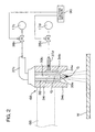
- Fig. 1 is a schematic sectional view illustrating the construction of a substrate treatment apparatus 1 according to one embodiment of the present invention, particularly illustrating a state thereof in a pretreatment process.
- the substrate treatment apparatus 1 is adapted to clean a surface of a semiconductor wafer W of silicon (herein after referred to simply as "wafer W"), and includes a spin base 10 for holding and rotating the wafer W, a bi-fluid nozzle 68 for supplying droplets of a pretreatment liquid onto the wafer W held by the spin base 10, a treatment liquid supplying section 7 for supplying a treatment liquid such as an etching liquid onto the wafer W held by the spin base 10, and a splash guard 50 for receiving treatment liquids (the pretreatment liquid, the etching liquid, water and the like) spun off from the wafer W held and rotated by the spin base 10.
- a spin base 10 for holding and rotating the wafer W
- a bi-fluid nozzle 68 for supplying droplets of a pretreatment liquid onto the wafer W held by the spin base 10
- a treatment liquid supplying section 7 for supplying a treatment liquid such as an etching liquid onto the wafer W held by the spin base 10
- the spin base 10 is a disk-shaped member, and includes a plurality of chuck pins 14 (e.g., six chuck pins 14) provided upright on the spin base for holding a peripheral portion of the round wafer W.
- the chuck pins 14 are provided equiangularly (e.g., at an angular interval of 60 degrees) about the center of the spin base 10 along the circumference of the spin base 10.
- the chuck pins 14 each include a substrate support 14a for supporting the peripheral portion of the wafer W from a lower side, and a substrate holder 14b for holding the wafer W by pressing the outer circumferential surface of the wafer W supported by the substrate supports 14a.
- the chuck pins 14 are adapted to be switched between a pressing state in which the substrate holders 14b are pressed against the outer circumferential surface of the wafer W and a non-pressing state in which the substrate holders 14b are spaced apart from the outer circumferential surface of the wafer W.
- the wafer W held by the chuck pins 14 is kept in a generally horizontal attitude.
- a hollow cylindrical rotation shaft 11 extends vertically from the center of a lower surface of the spin base 10.
- the rotation shaft 11 further extends downward through a plate base member 24 horizontally provided.
- a torque is transmitted to the rotation shaft 11 from a motor 20 mounted on the base member 24 via a belt drive mechanism 21.
- the belt drive mechanism 21 includes a driven pulley 21a attached to the rotation shaft 11, a driving pulley 21b attached to a rotation shaft of the motor 20, and a belt 21c stretched between the driven pulley 21a and the driving pulley 21b.
- the rotation shaft 11 is rotatable about a vertical axis J by a rotative driving force from the motor 20.
- the rotation shaft 11 is rotated, the spin base 10 and the wafer W held by the spin base 10 are rotated about the axis J.
- the belt drive mechanism 21 and the motor 20 are housed in a hollow cylindrical closed-top casing 25 provided on the base member 24.
- a hollow cylindrical partition member 27a is provided upright as surrounding the casing 25, and another hollow cylindrical partition member 27b is provided upright as surrounding the partition member 27a.
- a first liquid drain chamber 28 is defined between the casing 25 and the partition member 27a, which serve as side walls thereof.
- a second liquid drain chamber 29 is defined between the partition member 27a and the partition member 27b, which serve as side walls thereof.
- the first liquid drain chamber 28 has a V-shaped trench provided on the bottom thereof, and a drain port 28a provided in a middle portion of the V-shaped trench in communication with a waste drain 28b.
- the second liquid drain chamber 29 has a V-shaped trench provided on the bottom thereof, and a drain port 29a provided in a middle portion of the V-shaped trench in communication with a recovery drain 29b.
- the annular splash guard 50 as seen in plan is provided above the second liquid drain chamber 29.
- a groove-like first guide 51 having a chevron-shaped cross section is provided as opening inward in an upper interior portion of the splash guard 50.
- a second guide 52 having a quarter-circle-shaped cross section is provided as opening inwardly downward, and an annular groove 53 is formed as opening vertically downward in the innermost portion of the second guide 52.
- the splash guard 50 is coupled to a guard lift mechanism 55 via a link member 56 so as to be moved up and down by a driving force of the guard lift mechanism 55. When the splash guard 50 is moved down, the groove 53 is loosely engaged with an upper portion of the partition member 27a.
- the treatment liquid supplying section 7 includes a disk-shaped ambient shield plate 30, a tubular rotation shaft 35 extending vertically from the center of an upper surface of the ambient shield plate 30, and a treatment liquid pipe 36 extending within the rotation shaft 35.
- An opening having a diameter generally equal to the inner diameter of the rotation shaft 35 is formed in the center of the ambient shield plate 30.
- the rotation shaft 35 is rotatably supported by a support arm 40 via a bearing, and is coupled to a motor 42 attached to the support arm 40 via a belt drive mechanism 41.
- the belt drive mechanism 41 includes a driven pulley 41a attached to the rotation shaft 35, a driving pulley 41b attached to a rotation shaft of the motor 42, and a belt 41c stretched between the driven pulley 41a and the driving pulley 41b.
- the rotation shaft 35 is rotatable about the vertical axis J together with the ambient shield plate 30 by a rotative driving force from the motor 42. Therefore, the ambient shield plate 30 is rotated coaxially with the spin base 10 and the wafer W held by the spin base 10. The ambient shield plate 30 is rotated at substantially the same rotation speed as the wafer W held by the spin base 10.
- the belt drive mechanism 41 is housed within the support arm 40.
- the support arm 40 is connected to an arm lift mechanism 49 for up and down movement thereof.
- the treatment liquid supplying section 7 is movable between a proximate position at which it is located just above the wafer W held by the spin base 10 and a retracted position at which it is retracted apart from the wafer W held by the spin base 10. In Fig. 1, the treatment liquid supplying section 7 is located at the retracted position.
- the treatment liquid pipe 36 has an open lower end serving as a treatment liquid ejection port 36a, and an upper end connected to one end of a treatment liquid supply pipe 37.
- the other end of the treatment liquid supply pipe 37 is branched into a branch pipe 37a and a branch pipe 37b.
- a pure water supply source 17a for supplying pure water is connected in communication with the branch pipe 37a, and an etching liquid supply source 17b is connected in communication with the branch pipe 37b.
- the etching liquid supply source 17b supplies a solution mixture of hydrofluoric acid and hydrochloric acid as the etching liquid.
- Valves 38a and 38b are provided in the midst of the branch pipes 37a and 37b, respectively.
- the etching liquid and the pure water are selectively ejected from the treatment liquid ejection port 36a of the treatment liquid pipe 36. That is, the pure water can be supplied from the treatment liquid ejection port 36a by opening the valve 38a and closing the valve 38b.
- the etching liquid can be supplied from the treatment liquid ejection port 36a by opening the valve 38b and closing the valve 38a.
- a gap is present between an interior surface of the rotation shaft 35 and the treatment liquid pipe 36.
- This gap serves as a gas supply path 45.
- the gas supply path 45 has a lower end serving as a gas ejection port 45a and an upper end connected in communication with one end of a gas pipe 46.
- the other end of the gas pipe 46 is connected in communication with an inert gas supply source 23.
- the inert gas supply source 23 supplies nitrogen gas.
- a valve 47 is provided in the midst of the gas pipe 46. By opening the valve 47, the nitrogen gas can be supplied from the gas ejection port 45a.
- the bi-fluid nozzle 68 is movably provided between the spin base 10 and the ambient shield plate 30.
- the bi-fluid nozzle 68 is coupled to a nozzle movement mechanism 65 via a link member 66.
- the link member 66 is bent upward so as not to interfere with the splash guard 50 when the splash guard 50 is moved up.
- the nozzle movement mechanism 65 includes a motor 65a having a vertical rotation shaft P, and is capable of rotating the link member 66 and the bi-fluid nozzle 68 connected to the link member 66 about the rotation shaft P.
- the bi-fluid nozzle 68 is movable between an opposed position at which it is opposed to the wafer W held by the spin base 10 and a retracted position at which it is retracted laterally from the opposed position. At the opposed position, the bi-fluid nozzle 68 can be opposed to any portion from the center to the periphery of the wafer W held by the spin base 10.
- the nozzle movement mechanism 65 is connected to a nozzle lift mechanism 69, so that the bi-fluid nozzle 68 can be moved up and down together with the nozzle movement mechanism 65.
- the bi-fluid nozzle 68 is movable between the retracted position and the opposed position without interference with the splash guard 50 even when the splash guard 50 is moved up.
- Fig. 2 is a schematic sectional view illustrating the construction of the bi-fluid nozzle 68.
- the bi-fluid nozzle 68 includes a tubular liquid nozzle 39 and a tubular gas nozzle 34 surrounding the liquid nozzle 39, and has a generally cylindrical outer shape.
- the liquid nozzle 39 and the gas nozzle 34 have a common center axis Q and are coaxially positioned.
- An annular projection 34c is provided at one end of the gas nozzle 34 as projecting axially from the liquid nozzle 39.
- An inside portion of the liquid nozzle 39 serves as a liquid supply channel 39b.
- An annular space having the center axis Q is defined between the liquid nozzle 39 and the gas nozzle 34, and serves as a gas supply channel 34b.
- the gas supply channel 34b has an open end serving as a gas ejection port 34a on the side of the annular projection 34c of the bi-fluid nozzle 68.
- the gas supply channel 34b has a generally uniform diameter in an axially middle portion of the bi-fluid nozzle 68, but in the vicinity of the gas ejection port 34a, has a diameter decreasing toward the annular projection 34c so as to be convergent on a convergence point G which is located a predetermined distance apart from the gas ejection port 34a.
- the liquid supply channel 39b has an open end serving as a liquid ejection port 39a at the center of the gas ejection port 34a.
- the bi-fluid nozzle 68 is provided so that the liquid ejection port 39a and the gas ejection port 34a are directed downward.
- One end of a pretreatment liquid supply pipe 37c is connected to an end of the bi-fluid nozzle 68 opposite from the annular projection 34c in communication with the liquid nozzle 39.
- the other end of the pretreatment liquid supply pipe 37c is connected to a pretreatment liquid supply source 17c.
- the pretreatment liquid supply source 17c supplies a solution mixture of ammonia, hydrogen peroxide and water as the pretreatment liquid.
- One end of a compressed air supply pipe 37d is connected to a generally middle portion of a side wall of the bi-fluid nozzle 68 as seen along the center axis Q. An inside space of the compressed air supply pipe 37d communicates with the gas supply channel 34b.
- the other end of the compressed air supply pipe 37d is connected to a compressed air supply source 17d.
- a valve 38c is provided in the midst of the pretreatment liquid supply pipe 37c so as to control the opening and closing of the flow path of the pretreatment liquid and the flow rate of the pretreatment liquid.
- a valve 38d is provided in the midst of the compressed air supply pipe 37d so as to control the opening and closing of the flow path of the compressed air and the flow rate of the compressed air.
- the pretreatment liquid When the pretreatment liquid is supplied from the pretreatment liquid supply pipe 37c to the bi-fluid nozzle 68, the pretreatment liquid is ejected from the liquid ejection port 39a.
- the compressed air When the compressed air is supplied from the compressed air supply pipe 37d to the bi-fluid nozzle 68, the compressed air is ejected from the gas ejection port 34a.
- the ejected pretreatment liquid travels generally straight, while the compressed air annularly ejected travels as converging on the convergence point G.
- the pretreatment liquid and the compressed air are simultaneously supplied, the compressed air collides against the pretreatment liquid at the convergence point G.
- the pretreatment liquid is mixed with the compressed air thereby to be disintegrated into liquid droplets, which travel ahead while diverging slightly. That is, a jet of the droplets of the pretreatment liquid is provided.
- a method for cleaning the surface of the wafer W by means of the substrate treatment apparatus 1 will hereinafter be described.
- the guard lift mechanism 55 is controlled by the control section 90 so that an upper end of the splash guard 50 is generally leveled off at the spin base 10. Further, the nozzle movement mechanism 65 and the arm lift mechanism 49 are controlled by the control section 90 to move the bi-fluid nozzle 68 and the treatment liquid supplying section 7 to the retracted positions. In this state, a wafer W is transported onto the spin base 10 by a transportation robot not shown, and the chuck pins 14 are turned into the pressing state. Thus, the wafer W is held horizontally on the spin base 10 so that a surface thereof to be subjected to a cleaning process faces upward.
- the nozzle movement mechanism 65 is controlled by the control section 90 to locate the bi-fluid nozzle 68 at the opposed position.
- the guard lift mechanism 55 is controlled by the control section 90 to move up the splash guard 50 to a vertical position such that the spin base 10 and the wafer W held by the spin base 10 are laterally surrounded by the second guide 52. This state is shown in Fig. 1.
- the motor 20 is rotated by the control section 90, whereby the wafer W held by the spin base 10 is rotated. Further, the valves 38c, 38d are opened by the control section 90, whereby the pretreatment liquid and the compressed air are introduced into the bi-fluid nozzle 68. Thus, the droplets of the pretreatment liquid are generated and sprayed onto the surface of the wafer W.
- Fig. 3 is a schematic plan view for explaining the action of the bi-fluid nozzle 68 relative to the wafer W held by the spin base 10 in the pretreatment process.
- the bi-fluid nozzle 68 is moved along an arcuate path about the rotation shaft P of the motor 65a.
- the droplets of the pretreatment liquid are ejected toward the surface of the rotated wafer W, while the bi-fluid nozzle 68 is moved from a starting point K through the axis J to a final point F, wherein the starting point K is one of intersections between the arcuate path and the periphery of the wafer W, the axis J is the center and rotation center of the wafer W and the final point F is the other intersection.
- the entire surface of the wafer W is uniformly treated.
- the droplets of the pretreatment liquid can be bombarded against the surface of the wafer W with a great kinetic energy by introducing the high-pressure compressed air into the bi-fluid nozzle 68. At this time, particles adhering on the surface of the wafer W are physically removed by the kinetic energy of the droplets of the pretreatment liquid. The particles once removed from the surface of the wafer W do not easily adhere again onto the surface of the wafer W due to a repulsive force of a ⁇ potential.
- the pretreatment liquid is bombarded against the surface of the wafer W in a liquid droplet form (atomized form), so that the wafer W per se is not subjected to an excessively great load. Even if a pattern is formed on the surface of the wafer W, there is no possibility that the pattern is damaged. Further, the removal of the particles can be achieved in a shorter time by the physical cleaning.
- the surface of the wafer W is oxidized by the aforesaid solution mixture of ammonia, hydrogen peroxide and water as the pretreatment liquid.
- the thickness of an oxide layer to be formed on the surface of the wafer W can be controlled.
- the pretreatment process for the wafer W is achieved.
- the surface of the wafer W can shallowly be oxidized in a shorter time.
- copper (Cu) deposited as a metal deposit on the surface of the wafer W is dissolved in the form of an ammine complex by ammonia (aqueous ammonia) contained in the pretreatment liquid.
- the pretreatment liquid on the wafer W is spun off laterally of the wafer W by a centrifugal force, and received by the second guide 52 of the splash guard 50 (Fig. 1). Then, the pretreatment liquid flows down into the second drain chamber 29, and discharged into the recovery drain 29b through the drain port 29a.
- the pretreatment liquid discharged from the recovery drain 29b is collected in a recovery tank (not shown), and then supplied to the pretreatment liquid supply source 17c. Thus, the pretreatment liquid is recycled.
- Fig. 4 is a schematic sectional view illustrating a state of the substrate treatment apparatus 1 shown in Fig. 1 in an etching process.
- the etching process is performed.
- the guard lift mechanism 55 is controlled by the control section 90 to move down the splash guard 50 so that the spin base 10 and the wafer W held by the spin base 10 are surrounded by the first guide 51.
- the nozzle movement mechanism 65 and the nozzle lift mechanism 69 are controlled by the control section 90 so that the bi-fluid nozzle is retracted to the retracted position.
- the valve 38b is opened by the control section 90, so that the etching liquid is supplied to a center portion of the upper surface of the wafer W from the treatment liquid ejection port 36a.
- the surface layer of the wafer W oxidized with the pretreatment liquid is selectively etched with the solution mixture of hydrofluoric acid and hydrochloric acid as the etching liquid.
- the etching liquid containing hydrochloric acid in addition to hydrofluoric acid has a greater capability of dissolving the metal deposit. Therefore, metals deposited on the surface of the wafer W can advantageously be removed.
- the etching liquid is spun off from the wafer W by a centrifugal force, received by the first guide 51 of the splash guard 50, and then flows down into the first drain chamber 28.
- the etching liquid collected in the first drain chamber 28 is discharged into the waste drain 28b from the drain port 28a, and then discarded.
- Fig. 5 is a schematic sectional view illustrating a state of the substrate treatment apparatus 1 shown in Fig. 1 in the water rinsing process and the drying process.
- the valve 38b is closed by the control section 90 to stop the supply of the etching liquid. Then, the arm lift mechanism 49 and the motor 42 are controlled by the control section 90, so that the ambient shield plate 30 is positioned at the proximate position and rotated. In this state, the valves 38a and 47 are controlled to be opened by the control section 90.
- the pure water is supplied onto the surface of the wafer W from the treatment liquid ejection port 36a to rinse away the etching liquid.
- the nitrogen gas is supplied from the gas ejection port 45a, so that an oxygen partial pressure in a space between the ambient shield plate 30 and the wafer W is reduced.
- the water is spun off from the wafer W by a centrifugal force, received by the first guide 51 of the splash guard 50, and then flows down into the first drain chamber 28.
- the water collected in the first drain chamber 28 is discharged into the waste drain 28b from the drain port 28a, and then discarded.
- the valve 38a is controlled to be closed by the control section 90, so that the supply of the pure water is stopped.
- the supply of the nitrogen gas from the gas ejection port 45a is continued.
- the water is spun off from the surface of the wafer W for drying, while the space between the ambient shield plate 30 and the wafer W is kept at a reduced oxygen partial pressure.
- the valve 47 and the arm lift mechanism 49 are controlled by the control section 90 so as to stop the supply of the nitrogen gas and retract the treatment liquid supplying section 7 to the retracted position.
- the guard lift mechanism 55 is controlled by the control section 90, so that the upper end of the splash guard 50 is generally leveled off at the spin base 10. Then, the chuck pins 14 are turned into the non-pressing state, and the treated wafer W is transported out by the transportation robot not shown. Thus, the treatment of the surface of the single wafer W is completed.
- the pretreatment liquid and the etching liquid may be kept at an ordinary temperature, i.e., 20 to 28°C, preferably 20 to 25°C. That is, if the room is kept at an ordinary temperature, there is no particular need to adjust the temperatures of the pretreatment liquid and the etching liquid. Therefore, the treatment of the substrate can easily be performed.
- the etching liquid has a sufficiently great capability of dissolving the deposited metals, so that the substrate surface etch amount can be reduced.
- the deposited metals can be etched away in a shorter time. Therefore, the cleaning process from the removal of the particles to the removal of the deposited metals can be performed in a shorter time.
- an inert gas such as nitrogen gas may be employed instead of the compressed air when the droplets of the pretreatment liquid are generated by means of the bi-fluid nozzle 68.
- the gas compressed air
- a bi-fluid nozzle of an internal mixing type may be employed which is adapted to provide a jet of liquid droplets by mixing the pretreatment liquid with the gas within the nozzle.
- the pretreatment liquid supply source 17c may be adapted to supply a solution mixture containing ammonia and ozone water as the pretreatment liquid.
- a solution mixture containing ammonia and ozone water as the pretreatment liquid.
- the water rinsing process for rinsing the surface of the wafer W with pure water may also be performed between the pretreatment process and the etching process.
- a wafer cleaning test was performed with the use of the aforesaid substrate treatment apparatus 1.
- a solution mixture obtained by mixing an aqueous ammonia solution (29% solution), an aqueous hydrogen peroxide solution (30% solution) and water in a volume ratio of 1:1:5 was employed as the pretreatment liquid.
- a solution mixture obtained by mixing an aqueous hydrofluoric acid solution (50% solution), an aqueous hydrochloric acid solution (35% solution) and water in a volume ratio of 1:42:210 was employed as the etching liquid.
- the pretreatment liquid and the etching liquid each had a temperature of 23°C.
- the distance between the liquid ejection port 39a of the bi-fluid nozzle 68 and the convergence point G was not greater than 20 mm, and the distance between the convergence point G and the wafer W was 3 to 30 mm.
- the flow rate of the compressed air introduced into the bi-fluid nozzle 68 was 50 to 100 l/min, and the flow rate of the pretreatment liquid introduced into the bi-fluid nozzle 68 was 100 to 150 ml/min. Droplets of the pretreatment liquid provided under such conditions each had a diameter of about 5 to about 20 ⁇ m.
- the droplets of the pretreatment liquid were supplied (or the pretreatment liquid was sprayed) onto the surface of the wafer W, while the bi-fluid nozzle 68 was moved from the starting point K through the axis J to the final point F as shown in Fig. 3.
- the rotation speed of the spin base 10 was 10 to 1000 rpm.
- the etching liquid was supplied onto the center of the wafer W from the treatment liquid ejection port 36a for etching, while nitrogen gas was ejected from the gas ejection port 45a. Thereafter, pure water was supplied onto the center of the wafer W from the treatment liquid ejection port 36a for 10 seconds to rinse away the etching liquid. Then, the supply of the pure water was stopped, and the water was spun off by the rotation of the wafer W for drying.
- the time required for the aforesaid process sequence was sufficiently short, i.e., not longer than 100 seconds per wafer W.
- Fig. 6 is a diagram showing particle removal ratios at which particles of SiO 2 , Si, Al 2 O 3 , SiN and PSL (resin) were removed from the surface of the wafer W after the pretreatment process and after the etching process. Except the SiO 2 particles, not lower than about 90% of the particles were removed. These particle removal ratios are comparable to those provided by the multiple-wafer batch cleaning process in which a plurality of wafers W are simultaneously immersed in the treatment liquid for cleaning.
- Fig. 7 is a diagram showing the amounts of metals (Ca, Mn, Fe, Ni, Cu, Zn and Ti) deposited on the surface of the wafer W before and after the cleaning process.
- the analysis of the deposited metals was performed by employing a total reflection X-ray fluorescence analyzer (ditto in the following examples).
- the amounts of the deposited metals were 10 10 to 10 13 atoms/cm 2 before the cleaning process, but reduced below a detection limit (not greater than the order of 10 10 atoms/cm 2 ) after the cleaning process.
- the deposited metal amounts after the cleaning process were comparable to those provided by the multiple-wafer batch cleaning process.
- a wafer W employed in this cleaning test had a diameter of 8 inches, and was formed with a 200-nm (2000- ⁇ ) thick thermal oxide film (bare-Si), on which various kinds of metals (Ca, Mn, Fe, Ni, Cu, Zn and Ti) were forcibly deposited in an amount of about 4 ⁇ 10 10 to about 1 ⁇ 10 14 atoms/cm 2 and various kinds of particles (PSL, SiN, Al 2 O 3 , Si and SiO 2 ) were forcibly deposited in an amount of about 5000 to about 10000 particles.
- various kinds of metals Ca, Mn, Fe, Ni, Cu, Zn and Ti
- the pretreatment process was performed on the wafer W by the bi-fluid nozzle 68.
- the same conditions as in Example 1 were employed for the pretreatment process performed by the bi-fluid nozzle 68.
- pure water was ejected from the treatment liquid ejection port 36a for 20 seconds for rinsing the wafer W with the pure water (intermediate water rinsing) .
- the wafer W was subjected to the etching process.
- the time spent for supplying the etching liquid onto the wafer W from the treatment liquid ejection port 36a, i.e., the etching period was 20 seconds.
- pure water was supplied onto the center of the wafer W from the treatment liquid ejection port 36a for 40 seconds for rinsing the wafer W with the pure water. Then, the supply of the pure water was stopped, and the water was spun off for 20 seconds by rotating the wafer W for drying.
- Fig. 8 is a diagram showing particle removal ratios at which particles of PSL, SiN, Al 2 O 3 , Si and SiO 2 were removed from surfaces of wafers W after the cleaning process was performed by employing the pretreatment liquids having different compositions.
- the pretreatment liquid obtained by mixing the aqueous ammonia solution (29% solution), the aqueous hydrogen peroxide solution (30% solution) and water in a volume ratio of 1:1:5 was employed, the respective kinds of particles were removed at the highest removal ratios.
- the removal ratios of the PSL particles and the Si particles were particularly high as compared with the cases where the pretreatment liquids obtained by mixing the aqueous ammonia solution (29% solution), the aqueous hydrogen peroxide solution (30% solution) and water in volume ratios of 1:1:50 and 1:1:20, respectively, were employed.
- Fig. 9 is a diagram showing the amounts of metals (Ca, Mn, Fe, Ni, Cu, Zn and Ti) deposited on the surface of the wafer W after the cleaning process when the pretreatment liquid obtained by mixing the aqueous ammonia solution (29% solution), the aqueous hydrogen peroxide solution (30% solution) and water in a volume ratio of 1:1:5 was employed for the pretreatment process.
- metals Ca, Mn, Fe, Ni, Cu, Zn and Ti
- the amounts of the respective kinds of deposited metals were reduced below the detection limit (on the order of 1 ⁇ 10 10 ) after the cleaning process.
- a solution mixture obtained by mixing an aqueous ammonia solution (29% solution), an aqueous hydrogen peroxide solution (30% solution) and water in a volume ratio of 1:1:5 was employed as the pretreatment liquid.
- a solution mixture obtained by mixing an aqueous hydrofluoric acid solution (50% solution), an aqueous hydrochloric acid solution (35% solution) and water in a volume ratio of 1:41:207 was employed as the etching liquid.
- the pretreatment liquid and the etching liquid each had a temperature of 23°C.
- the pretreatment process was performed on the wafer W by the bi-fluid nozzle 68.
- the same conditions as in Example 1 were employed for the pretreatment process performed by the bi-fluid nozzle 68.
- five pretreatment periods i.e., 5 seconds, 10 seconds, 15 seconds, 20 seconds and 30 seconds, were employed.
- the wafer W was subjected to the etching process.
- the etching period was 20 seconds.
- the wafer W was rinsed with pure water for 30 seconds. Then, the supply of the pure water was stopped, and the water was spun off for 20 seconds by rotating the wafer W for drying.
- Fig. 10 is a diagram showing relationships between the pretreatment period and the particle removal ratio at which particles were removed from the surface of the wafer W.
- the removal ratio was generally increased with the pretreatment period, and was at a plateau when the pretreatment period was 20 seconds or longer.
- the pretreatment process can be completed in a pretreatment period of 20 seconds.
- a solution mixture obtained by mixing an aqueous ammonia solution (29% solution), an aqueous hydrogen peroxide solution (30% solution) and water in a volume ratio of 1:1:5 was employed as the pretreatment liquid.
- Three solution mixtures obtained by mixing an aqueous hydrofluoric acid solution (50% solution), an aqueous hydrochloric acid solution (35% solution) and water in a volume ratio of 0.5:41:207, 1:41:207 and 2:41:207 hereinafter referred to as "0.5:41:207 solution”, “1:41:207 solution” and “2:41:207 solution", respectively) were employed as the etching liquid.
- the pretreatment liquid and the etching liquid each had a temperature of 23°C.
- the pretreatment process was performed on the wafer W for 20 seconds by the bi-fluid nozzle 68.
- the same conditions as in Example 1 were employed for the pretreatment process performed by the bi-fluid nozzle 68.
- the etching process was performed on the wafer W with the use of the etching liquid.
- two etching periods i.e., 20 seconds and 40 seconds, were employed.
- two etching periods i.e., 10 seconds and 20 seconds
- three etching periods i.e., 5 seconds, 10 seconds and 20 seconds, were employed.
- the wafer W was rinsed with pure water for 30 seconds. Then, the supply of the pure water was stopped, and the water was spun off for 20 seconds by rotating the wafer W for drying.
- Fig. 11 is a diagram showing the amounts of copper deposited on the surface of the wafer W before and after the cleaning process was performed with the respective etching periods.
- the deposited copper amount was about 10 13 to about 10 14 atoms/cm 2 before the cleaning process, but reduced as the etching period was increased.
- the deposited copper amount was sufficiently reduced to about 10 10 atoms/cm 2 with an etching period of 20 seconds.
- the 0.5:41:207 solution was employed as the etching liquid, the deposited copper amount was sufficiently reduced to about 10 10 atoms/cm 2 with an etching period of 40 seconds.
- the etching process can be completed in an etching period of 20 seconds where the 1:41:207 solution was employed.
- a relationship between the wafer etching period and the etch thickness was checked with the use of the aforesaid substrate treatment apparatus 1.
- the wafer W was not subjected to the pretreatment process prior to the etching process.
- a 1:41:207 solution was employed as the etching liquid.
- the etching liquid had a temperature of 23°C.
- Fig. 12 is a diagram showing the relationship between the wafer etching period and the etch thickness.
- the etch thickness was generally linearly increased with the etching period. Where the etching period was 20 seconds, the etch thickness was suppressed to about 2.5 ⁇ .
- a solution mixture obtained by mixing an aqueous ammonia solution (29% solution), an aqueous hydrogen peroxide solution (30% solution) and water in a volume ratio of 1:1:5 was employed as the pretreatment liquid.
- a solution mixture obtained by mixing an aqueous hydrofluoric acid solution (50% solution), an aqueous hydrochloric acid solution (35% solution) and water in a volume ratio of 1:41:207 was employed as the etching liquid.
- the pretreatment liquid and the etching liquid each had a temperature of 23°C.
- the pretreatment process was performed on the wafer W by the bi-fluid nozzle 68.
- the same conditions as in Example 1 were employed for the pretreatment process performed by the bi-fluid nozzle 68.
- the pretreatment period was 20 seconds.
- the wafer W was subjected to the etching process.
- the etching period was 20 seconds.
- the wafer W was rinsed with water.
- Four water rinsing periods i.e., 0 second, 20 seconds, 30 seconds and 60 seconds, were employed for the water rinsing process. Thereafter, the water was spun off for 20 seconds by rotating the wafer W for drying.
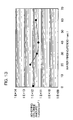
- Fig. 13 is a diagram showing the amounts of chlorine on the surface of the wafer W after the cleaning process was performed with the respective water rinsing periods.
- the chlorine detection limit was about 2.0 ⁇ 10 11 atoms/cm 2 .
- the chlorine amount was about 8 ⁇ 10 11 atoms/cm 2 when the water rinsing process was not performed after the etching process, and generally reduced as the water rinsing period was increased. Where the water rinsing period was 30 seconds or longer, the chlorine amount was not greater than about 4 ⁇ 10 11 atoms/cm 2 . This is comparable to a chlorine amount (about 3 ⁇ 10 11 atoms/cm 2 ) observed after the wafer W is rinsed with water by the multiple-wafer batch process.
- the intermediate water rinsing process was not performed after the pretreatment process before the etching process, but the deposited metal amounts and the particle amounts after the cleaning process were sufficiently low. This indicates that the intermediate water rinsing process may be obviated.
- the cleaning test was performed with the use of wafers W on which the metals and the particles were forcibly deposited, and optimum cleaning conditions for a naturally contaminated wafer W may be different from the aforesaid conditions.
- the cleaning conditions may be changed within wide ranges of conditions specified by the present invention, so that the naturally contaminated wafer W can also properly be cleaned by changing the cleaning conditions depending on the kinds and amounts of metals and particles deposited on the wafer.
- a wafer cleaning test was performed with the use of the aforesaid substrate treatment apparatus 1.
- a solution mixture obtained by mixing an aqueous ammonia solution (29% solution) and ozone water having an ozone concentration of 5 to 30 ppm in a volume ratio of 1:5 was employed as the pretreatment liquid.
- a solution mixture obtained by mixing an aqueous hydrofluoric acid solution (50% solution), an aqueous hydrochloric acid solution (35% solution) and water in a volume ratio of 1:42:210 was employed as the etching liquid.
- the pretreatment liquid and the etching liquid each had a temperature of 23°C.
- the distance between the liquid ejection port 39a of the bi-fluid nozzle 68 and the convergence point G was not greater than 20 mm, and the distance between the convergence point G and the wafer W was 3 to 30 mm.
- the flow rate of the compressed air introduced into the bi-fluid nozzle 68 was 50 to 100 l/min, and the flow rate of the pretreatment liquid introduced into the bi-fluid nozzle 68 was 100 to 150 ml/min. Droplets of the pretreatment liquid provided under such conditions each had a diameter of about 5 to about 20 ⁇ m.
- the droplets of the pretreatment liquid were supplied (or the pretreatment liquid was sprayed) onto the surface of the wafer W, while the bi-fluid nozzle 68 was moved from the starting point K through the axis J to the final point F as shown in Fig. 3.
- the rotation speed of the spin base 10 was 10 to 1000 rpm.
- the etching liquid was supplied onto the center of the wafer W from the treatment liquid ejection port 36a for etching, while nitrogen gas was ejected from the gas ejection port 45a. Thereafter, pure water was supplied onto the center of the wafer W from the treatment liquid ejection port 36a for 10 seconds to rinse away the etching liquid. Then, the supply of the pure water was stopped, and the water was spun off by the rotation of the wafer W for drying.
Applications Claiming Priority (6)
| Application Number | Priority Date | Filing Date | Title |
|---|---|---|---|
| JP2002022089 | 2002-01-30 | ||
| JP2002022089 | 2002-01-30 | ||
| JP2002086359 | 2002-03-26 | ||
| JP2002086359 | 2002-03-26 | ||
| JP2002365653 | 2002-12-17 | ||
| JP2002365653A JP4074814B2 (ja) | 2002-01-30 | 2002-12-17 | 基板処理装置および基板処理方法 |
Publications (3)
| Publication Number | Publication Date |
|---|---|
| EP1335412A2 true EP1335412A2 (fr) | 2003-08-13 |
| EP1335412A3 EP1335412A3 (fr) | 2006-06-14 |
| EP1335412B1 EP1335412B1 (fr) | 2008-02-27 |
Family
ID=27617311
Family Applications (1)
| Application Number | Title | Priority Date | Filing Date |
|---|---|---|---|
| EP03001859A Expired - Lifetime EP1335412B1 (fr) | 2002-01-30 | 2003-01-29 | Dispositif et procédé de traitement de substrat |
Country Status (5)
| Country | Link |
|---|---|
| US (1) | US20030170988A1 (fr) |
| EP (1) | EP1335412B1 (fr) |
| JP (1) | JP4074814B2 (fr) |
| KR (1) | KR100537668B1 (fr) |
| DE (1) | DE60319294T2 (fr) |
Cited By (6)
| Publication number | Priority date | Publication date | Assignee | Title |
|---|---|---|---|---|
| EP1848025A1 (fr) * | 2006-04-18 | 2007-10-24 | Tokyo Electron Limited | Appareil de traitement de liquides |
| EP1848024A1 (fr) * | 2006-04-18 | 2007-10-24 | Tokyo Electron Limited | Appareil de traitement de liquides |
| CN100466190C (zh) * | 2004-03-12 | 2009-03-04 | 禧沛股份有限公司 | 基片处理装置 |
| WO2009139826A2 (fr) * | 2008-05-12 | 2009-11-19 | Fsi International, Inc. | Systèmes de traitement de substrat et procédés associés |
| EP2154716A3 (fr) * | 2008-08-11 | 2010-03-24 | Murata Machinery, Ltd. | Buse |
| US9666456B2 (en) | 2006-07-07 | 2017-05-30 | Tel Fsi, Inc. | Method and apparatus for treating a workpiece with arrays of nozzles |
Families Citing this family (41)
| Publication number | Priority date | Publication date | Assignee | Title |
|---|---|---|---|---|
| US20070066076A1 (en) * | 2005-09-19 | 2007-03-22 | Bailey Joel B | Substrate processing method and apparatus using a combustion flame |
| US7524771B2 (en) * | 2002-10-29 | 2009-04-28 | Dainippon Screen Mfg. Co., Ltd. | Substrate processing method using alkaline solution and acid solution |
| US20040235308A1 (en) * | 2003-05-22 | 2004-11-25 | Dainippon Screen Mfg. Co., Ltd. | Substrate treatment method and sustrate treatment apparatus |
| JP4494840B2 (ja) * | 2003-06-27 | 2010-06-30 | 大日本スクリーン製造株式会社 | 異物除去装置、基板処理装置および基板処理方法 |
| GB2412351A (en) * | 2004-03-24 | 2005-09-28 | Esselte | A tape printer having separate tape and ink ribbon cassettes |
| WO2006107550A2 (fr) * | 2005-04-01 | 2006-10-12 | Fsi International, Inc. | Structure barriere et dispositif de buses pour outils de traitement de pieces microelectroniques par fluides |
| US20060237043A1 (en) * | 2005-04-25 | 2006-10-26 | Applied Materials, Inc. | Method and apparatus for cleaning semiconductor substrates |
| JP4763575B2 (ja) * | 2006-01-26 | 2011-08-31 | 大日本スクリーン製造株式会社 | 基板処理装置および基板処理方法 |
| JP4767767B2 (ja) * | 2006-06-19 | 2011-09-07 | 大日本スクリーン製造株式会社 | 基板処理方法および基板処理装置 |
| US20080135070A1 (en) * | 2006-12-12 | 2008-06-12 | Wei Lu | Method and apparatus for active particle and contaminant removal in wet clean processes in semiconductor manufacturing |
| US20080230092A1 (en) * | 2007-03-23 | 2008-09-25 | Alexander Sou-Kang Ko | Method and apparatus for single-substrate cleaning |
| KR20090005489A (ko) | 2007-07-09 | 2009-01-14 | 삼성전자주식회사 | 반도체 습식 에천트 및 그를 이용한 배선 구조체의형성방법 |
| CN101802975B (zh) * | 2007-08-07 | 2012-10-03 | Fsi国际公司 | 在用于通过一种或多种处理流体来处理微电子工件的工具中的阻挡板和文氏管容纳系统的漂洗方法以及相关装置 |
| US20090255555A1 (en) * | 2008-04-14 | 2009-10-15 | Blakely, Sokoloff, Taylor & Zafman | Advanced cleaning process using integrated momentum transfer and controlled cavitation |
| KR100968584B1 (ko) * | 2008-04-14 | 2010-07-08 | 포항공과대학교 산학협력단 | 액적 토출 장치 |
| KR101652270B1 (ko) * | 2008-05-09 | 2016-08-30 | 티이엘 에프에스아이, 인코포레이티드 | 개방 동작 모드와 폐쇄 동작 모드사이를 용이하게 변경하는 처리실 설계를 이용하여 마이크로일렉트로닉 워크피이스를 처리하는 장치 및 방법 |
| CN101643904B (zh) * | 2009-08-27 | 2011-04-27 | 北京北方微电子基地设备工艺研究中心有限责任公司 | 深硅刻蚀装置和深硅刻蚀设备的进气系统 |
| JP2012074601A (ja) * | 2010-09-29 | 2012-04-12 | Dainippon Screen Mfg Co Ltd | 基板処理装置および基板処理方法 |
| KR101212803B1 (ko) * | 2010-10-01 | 2012-12-14 | 주식회사 엠엠테크 | 표면을 에칭할 수 있는 실리콘 기판의 처리 장치 |
| KR101212804B1 (ko) * | 2010-10-01 | 2012-12-14 | 주식회사 엠엠테크 | 콤팩트한 구조를 갖는 실리콘 기판의 처리 장치 |
| US8791026B2 (en) | 2010-10-01 | 2014-07-29 | Mmtech Co., Ltd. | Method and apparatus for treating silicon substrate |
| KR101252752B1 (ko) * | 2010-10-01 | 2013-04-09 | 주식회사 엠엠테크 | 실리콘 기판의 처리방법 및 처리 장치 |
| CN102560494B (zh) * | 2010-12-30 | 2014-06-25 | 富葵精密组件(深圳)有限公司 | 蚀刻装置及蚀刻方法 |
| JP5829082B2 (ja) * | 2011-09-09 | 2015-12-09 | オリンパス株式会社 | 洗浄装置 |
| CA2856196C (fr) | 2011-12-06 | 2020-09-01 | Masco Corporation Of Indiana | Distribution d'ozone dans un robinet |
| US10604302B2 (en) | 2012-11-20 | 2020-03-31 | Altria Client Services Llc | Polymer coated paperboard container and method |
| JP6017999B2 (ja) * | 2013-03-15 | 2016-11-02 | 株式会社Screenホールディングス | 基板処理装置 |
| US10707099B2 (en) | 2013-08-12 | 2020-07-07 | Veeco Instruments Inc. | Collection chamber apparatus to separate multiple fluids during the semiconductor wafer processing cycle |
| US9768041B2 (en) | 2013-08-12 | 2017-09-19 | Veeco Precision Surface Processing Llc | Collection chamber apparatus to separate multiple fluids during the semiconductor wafer processing cycle |
| JP6523643B2 (ja) | 2014-09-29 | 2019-06-05 | 株式会社Screenホールディングス | 基板処理装置および基板処理方法 |
| KR101621482B1 (ko) * | 2014-09-30 | 2016-05-17 | 세메스 주식회사 | 기판 처리 장치 및 방법 |
| CN108463437B (zh) | 2015-12-21 | 2022-07-08 | 德尔塔阀门公司 | 包括消毒装置的流体输送系统 |
| JP6614610B2 (ja) * | 2016-02-12 | 2019-12-04 | 株式会社Screenホールディングス | 基板処理装置 |
| US20170287743A1 (en) * | 2016-03-31 | 2017-10-05 | Shibaura Mechatronics Corporation | Substrate treating device and substrate treating method |
| JP6934732B2 (ja) * | 2016-03-31 | 2021-09-15 | 芝浦メカトロニクス株式会社 | 基板処理装置及び基板処理方法 |
| DE102016210883A1 (de) * | 2016-06-17 | 2017-12-21 | Singulus Technologies Ag | Vorrichtung und Verfahren zur Behandlung von Substraten unter Verwendung einer Auflagerolle mit porösem Material |
| TWI797121B (zh) | 2017-04-25 | 2023-04-01 | 美商維克儀器公司 | 半導體晶圓製程腔體 |
| KR102388407B1 (ko) | 2019-07-02 | 2022-04-21 | 세메스 주식회사 | 노즐 장치, 기판 처리 장치 및 방법 |
| CN112670207B (zh) * | 2020-12-21 | 2023-10-31 | 长江存储科技有限责任公司 | 晶边处理设备及待处理晶圆结构的处理方法 |
| CN112967995B (zh) * | 2021-02-01 | 2022-12-30 | 泉芯集成电路制造(济南)有限公司 | 一种芯片夹具、芯片清洗装置及芯片刻蚀装置 |
| CN115299374B (zh) * | 2022-09-07 | 2023-08-01 | 漳浦县赵木兰养殖有限公司 | 一种用于后备猪诱情期的设备 |
Citations (10)
| Publication number | Priority date | Publication date | Assignee | Title |
|---|---|---|---|---|
| EP0294690A2 (fr) * | 1987-06-12 | 1988-12-14 | International Business Machines Corporation | Pulvérisateur pour liquide de nettoyage et sa méthode d'utilisation |
| JPH04346431A (ja) * | 1991-05-24 | 1992-12-02 | Mitsubishi Electric Corp | 半導体シリコンウェハの洗浄装置 |
| US5454901A (en) * | 1990-05-22 | 1995-10-03 | Nec Corporation | Process for treating semiconductor substrates |
| US5679171A (en) * | 1995-03-27 | 1997-10-21 | Sony Corporation | Method of cleaning substrate |
| EP0805484A1 (fr) * | 1995-01-13 | 1997-11-05 | Daikin Industries, Limited | Procede de nettoyage de substrats |
| JPH10256211A (ja) * | 1997-03-11 | 1998-09-25 | Sony Corp | 半導体基板の洗浄方法 |
| US5918817A (en) * | 1996-12-02 | 1999-07-06 | Mitsubishi Denki Kabushiki Kaisha | Two-fluid cleaning jet nozzle and cleaning apparatus, and method utilizing the same |
| US5934566A (en) * | 1995-05-26 | 1999-08-10 | Mitsubishi Denki Kabushiki Kaisha | Washing apparatus and washing method |
| EP1091388A2 (fr) * | 1999-10-06 | 2001-04-11 | Ebara Corporation | Procédé et dispositif pour le nettoyage d'un substrat |
| US20010052354A1 (en) * | 1999-08-25 | 2001-12-20 | Shibaura Mechatronics Corporation | Apparatus for processing substrate using process solutions having desired mixing ratios |
Family Cites Families (9)
| Publication number | Priority date | Publication date | Assignee | Title |
|---|---|---|---|---|
| JPH1154471A (ja) * | 1997-08-05 | 1999-02-26 | Tokyo Electron Ltd | 処理装置及び処理方法 |
| JP3920429B2 (ja) * | 1997-12-02 | 2007-05-30 | 株式会社ルネサステクノロジ | 位相シフトフォトマスクの洗浄方法および洗浄装置 |
| JP2001033938A (ja) * | 1999-07-22 | 2001-02-09 | Oki Electric Ind Co Ltd | ハーフトーン位相シフトマスクの特性補正方法 |
| JP2001237208A (ja) * | 2000-02-24 | 2001-08-31 | Ebara Corp | 研磨装置の研磨面洗浄方法及び洗浄装置 |
| JP3875456B2 (ja) * | 2000-06-29 | 2007-01-31 | 株式会社東芝 | 洗浄方法および洗浄装置 |
| US6951221B2 (en) * | 2000-09-22 | 2005-10-04 | Dainippon Screen Mfg. Co., Ltd. | Substrate processing apparatus |
| US6705331B2 (en) * | 2000-11-20 | 2004-03-16 | Dainippon Screen Mfg., Co., Ltd. | Substrate cleaning apparatus |
| JP4210045B2 (ja) * | 2001-06-25 | 2009-01-14 | 横河電機株式会社 | 洗浄装置 |
| US6726848B2 (en) * | 2001-12-07 | 2004-04-27 | Scp Global Technologies, Inc. | Apparatus and method for single substrate processing |
-
2002
- 2002-12-17 JP JP2002365653A patent/JP4074814B2/ja not_active Expired - Fee Related
-
2003
- 2003-01-28 US US10/353,172 patent/US20030170988A1/en not_active Abandoned
- 2003-01-29 EP EP03001859A patent/EP1335412B1/fr not_active Expired - Lifetime
- 2003-01-29 DE DE60319294T patent/DE60319294T2/de not_active Expired - Lifetime
- 2003-01-29 KR KR10-2003-0005754A patent/KR100537668B1/ko not_active IP Right Cessation
Patent Citations (10)
| Publication number | Priority date | Publication date | Assignee | Title |
|---|---|---|---|---|
| EP0294690A2 (fr) * | 1987-06-12 | 1988-12-14 | International Business Machines Corporation | Pulvérisateur pour liquide de nettoyage et sa méthode d'utilisation |
| US5454901A (en) * | 1990-05-22 | 1995-10-03 | Nec Corporation | Process for treating semiconductor substrates |
| JPH04346431A (ja) * | 1991-05-24 | 1992-12-02 | Mitsubishi Electric Corp | 半導体シリコンウェハの洗浄装置 |
| EP0805484A1 (fr) * | 1995-01-13 | 1997-11-05 | Daikin Industries, Limited | Procede de nettoyage de substrats |
| US5679171A (en) * | 1995-03-27 | 1997-10-21 | Sony Corporation | Method of cleaning substrate |
| US5934566A (en) * | 1995-05-26 | 1999-08-10 | Mitsubishi Denki Kabushiki Kaisha | Washing apparatus and washing method |
| US5918817A (en) * | 1996-12-02 | 1999-07-06 | Mitsubishi Denki Kabushiki Kaisha | Two-fluid cleaning jet nozzle and cleaning apparatus, and method utilizing the same |
| JPH10256211A (ja) * | 1997-03-11 | 1998-09-25 | Sony Corp | 半導体基板の洗浄方法 |
| US20010052354A1 (en) * | 1999-08-25 | 2001-12-20 | Shibaura Mechatronics Corporation | Apparatus for processing substrate using process solutions having desired mixing ratios |
| EP1091388A2 (fr) * | 1999-10-06 | 2001-04-11 | Ebara Corporation | Procédé et dispositif pour le nettoyage d'un substrat |
Non-Patent Citations (2)
| Title |
|---|
| PATENT ABSTRACTS OF JAPAN vol. 017, no. 203 (E-1354), 21 April 1993 (1993-04-21) -& JP 04 346431 A (MITSUBISHI ELECTRIC CORP), 2 December 1992 (1992-12-02) * |
| PATENT ABSTRACTS OF JAPAN vol. 1998, no. 14, 31 December 1998 (1998-12-31) -& JP 10 256211 A (SONY CORP), 25 September 1998 (1998-09-25) * |
Cited By (13)
| Publication number | Priority date | Publication date | Assignee | Title |
|---|---|---|---|---|
| CN100466190C (zh) * | 2004-03-12 | 2009-03-04 | 禧沛股份有限公司 | 基片处理装置 |
| KR101019444B1 (ko) | 2006-04-18 | 2011-03-07 | 도쿄엘렉트론가부시키가이샤 | 액 처리 장치 |
| EP1848024A1 (fr) * | 2006-04-18 | 2007-10-24 | Tokyo Electron Limited | Appareil de traitement de liquides |
| EP1848025A1 (fr) * | 2006-04-18 | 2007-10-24 | Tokyo Electron Limited | Appareil de traitement de liquides |
| US7998308B2 (en) | 2006-04-18 | 2011-08-16 | Tokyo Electron Limited | Liquid processing apparatus |
| US7793610B2 (en) | 2006-04-18 | 2010-09-14 | Tokyo Electron Limited | Liquid processing apparatus |
| US9666456B2 (en) | 2006-07-07 | 2017-05-30 | Tel Fsi, Inc. | Method and apparatus for treating a workpiece with arrays of nozzles |
| WO2009139826A2 (fr) * | 2008-05-12 | 2009-11-19 | Fsi International, Inc. | Systèmes de traitement de substrat et procédés associés |
| WO2009139826A3 (fr) * | 2008-05-12 | 2010-04-01 | Fsi International, Inc. | Systèmes de traitement de substrat et procédés associés |
| US8235068B2 (en) | 2008-05-12 | 2012-08-07 | Fsi International, Inc. | Substrate processing systems and related methods |
| US8408253B2 (en) | 2008-08-11 | 2013-04-02 | Murata Machinery, Ltd. | Nozzle |
| TWI454317B (zh) * | 2008-08-11 | 2014-10-01 | Murata Machinery Ltd | nozzle |
| EP2154716A3 (fr) * | 2008-08-11 | 2010-03-24 | Murata Machinery, Ltd. | Buse |
Also Published As
| Publication number | Publication date |
|---|---|
| DE60319294T2 (de) | 2008-05-29 |
| JP2004006618A (ja) | 2004-01-08 |
| EP1335412A3 (fr) | 2006-06-14 |
| DE60319294D1 (de) | 2008-04-10 |
| EP1335412B1 (fr) | 2008-02-27 |
| US20030170988A1 (en) | 2003-09-11 |
| KR100537668B1 (ko) | 2005-12-19 |
| JP4074814B2 (ja) | 2008-04-16 |
| KR20030065394A (ko) | 2003-08-06 |
Similar Documents
| Publication | Publication Date | Title |
|---|---|---|
| EP1335412B1 (fr) | Dispositif et procédé de traitement de substrat | |
| US9984903B2 (en) | Treatment cup cleaning method, substrate treatment method, and substrate treatment apparatus | |
| KR100848981B1 (ko) | 기판처리방법 및 기판처리장치 | |
| US5487398A (en) | Rotary cleaning method with chemical solutions and rotary cleaning apparatus with chemical solutions | |
| JP4638402B2 (ja) | 二流体ノズル、ならびにそれを用いた基板処理装置および基板処理方法 | |
| US7524771B2 (en) | Substrate processing method using alkaline solution and acid solution | |
| CN108701606B (zh) | 基板处理方法及基板处理装置 | |
| CN108701609B (zh) | 基板处理方法及基板处理装置 | |
| US20230352321A1 (en) | Wet processing of microelectronic substrates with controlled mixing of fluids proximal to substrate surfaces | |
| JP4976949B2 (ja) | 基板処理装置 | |
| US20080314870A1 (en) | Substrate Processing Method, Substrate Processing Apparatus, and Control Program | |
| US9892955B2 (en) | Substrate holding/rotating device, substrate processing apparatus including the same, and substrate processing method | |
| KR20070041342A (ko) | 기판처리방법 및 기판처리장치 | |
| US10622225B2 (en) | Substrate processing apparatus and nozzle cleaning method | |
| TWI631996B (zh) | Substrate processing method and substrate processing device | |
| US7364625B2 (en) | Rinsing processes and equipment | |
| US9275849B2 (en) | Single-chamber apparatus for precision cleaning and drying of flat objects | |
| JP5954862B2 (ja) | 基板処理装置 | |
| JP2008108830A (ja) | 二流体ノズルユニットおよびそれを用いた基板処理装置 | |
| WO2014116440A1 (fr) | Procédé d'élimination de matière carbonée de substrats | |
| EP1758689A2 (fr) | Système et méthode de traitement de séchage de liquide sur une ou plusieurs galettes | |
| US20090241998A1 (en) | Apparatus for foam-assisted wafer cleaning with use of universal fluid supply unit | |
| JP4702920B2 (ja) | 基板処理方法および基板処理装置 | |
| WO2017164186A1 (fr) | Procédé de traitement de substrat et dispositif de traitement de substrat | |
| JP4781253B2 (ja) | 基板処理装置および基板処理方法 |
Legal Events
| Date | Code | Title | Description |
|---|---|---|---|
| PUAI | Public reference made under article 153(3) epc to a published international application that has entered the european phase |
Free format text: ORIGINAL CODE: 0009012 |
|
| AK | Designated contracting states |
Designated state(s): AT BE BG CH CY CZ DE DK EE ES FI FR GB GR HU IE IT LI LU MC NL PT SE SI SK TR |
|
| AX | Request for extension of the european patent |
Extension state: AL LT LV MK RO |
|
| PUAL | Search report despatched |
Free format text: ORIGINAL CODE: 0009013 |
|
| AK | Designated contracting states |
Kind code of ref document: A3 Designated state(s): AT BE BG CH CY CZ DE DK EE ES FI FR GB GR HU IE IT LI LU MC NL PT SE SI SK TR |
|
| AX | Request for extension of the european patent |
Extension state: AL LT LV MK RO |
|
| 17P | Request for examination filed |
Effective date: 20060921 |
|
| AKX | Designation fees paid |
Designated state(s): DE FR |
|
| 17Q | First examination report despatched |
Effective date: 20070206 |
|
| GRAP | Despatch of communication of intention to grant a patent |
Free format text: ORIGINAL CODE: EPIDOSNIGR1 |
|
| GRAS | Grant fee paid |
Free format text: ORIGINAL CODE: EPIDOSNIGR3 |
|
| GRAA | (expected) grant |
Free format text: ORIGINAL CODE: 0009210 |
|
| AK | Designated contracting states |
Kind code of ref document: B1 Designated state(s): DE FR |
|
| RIN1 | Information on inventor provided before grant (corrected) |
Inventor name: IZUMI, AKIRA,C/O DAINIPPON SCREEN MFG. CO., LTD. Inventor name: KIYOSE, HIROMI,C/O DAINIPPON SCREEN MFG. CO., LTD Inventor name: NOGUCHI, SACHIKO,DAINIPPON SCREEN MFG. CO., LTD. |
|
| REF | Corresponds to: |
Ref document number: 60319294 Country of ref document: DE Date of ref document: 20080410 Kind code of ref document: P |
|
| RIN2 | Information on inventor provided after grant (corrected) |
Inventor name: IZUMI, AKIRA,C/O DAINIPPON SCREEN MFG. CO., LTD. Inventor name: KIYOSE, HIROMI,C/O DAINIPPON SCREEN MFG. CO., LTD Inventor name: NOGUCHI, SACHIKO,C/O DAINIPPON SCREEN MFG. CO., LT |
|
| ET | Fr: translation filed | ||
| PLBE | No opposition filed within time limit |
Free format text: ORIGINAL CODE: 0009261 |
|
| STAA | Information on the status of an ep patent application or granted ep patent |
Free format text: STATUS: NO OPPOSITION FILED WITHIN TIME LIMIT |
|
| 26N | No opposition filed |
Effective date: 20081128 |
|
| PGFP | Annual fee paid to national office [announced via postgrant information from national office to epo] |
Ref country code: FR Payment date: 20100208 Year of fee payment: 8 |
|
| PGFP | Annual fee paid to national office [announced via postgrant information from national office to epo] |
Ref country code: DE Payment date: 20100121 Year of fee payment: 8 |
|
| REG | Reference to a national code |
Ref country code: FR Ref legal event code: ST Effective date: 20110930 |
|
| PG25 | Lapsed in a contracting state [announced via postgrant information from national office to epo] |
Ref country code: FR Free format text: LAPSE BECAUSE OF NON-PAYMENT OF DUE FEES Effective date: 20110131 |
|
| REG | Reference to a national code |
Ref country code: DE Ref legal event code: R119 Ref document number: 60319294 Country of ref document: DE Effective date: 20110802 |
|
| PG25 | Lapsed in a contracting state [announced via postgrant information from national office to epo] |
Ref country code: DE Free format text: LAPSE BECAUSE OF NON-PAYMENT OF DUE FEES Effective date: 20110802 |