EP1333498B1 - Solid state image sensor array for correcting curvilinear distortion of a camera lens system and method for fabricating the image sensor array - Google Patents
Solid state image sensor array for correcting curvilinear distortion of a camera lens system and method for fabricating the image sensor array Download PDFInfo
- Publication number
- EP1333498B1 EP1333498B1 EP02021760A EP02021760A EP1333498B1 EP 1333498 B1 EP1333498 B1 EP 1333498B1 EP 02021760 A EP02021760 A EP 02021760A EP 02021760 A EP02021760 A EP 02021760A EP 1333498 B1 EP1333498 B1 EP 1333498B1
- Authority
- EP
- European Patent Office
- Prior art keywords
- sensor array
- image sensor
- line segments
- photosensitive elements
- straight line
- Prior art date
- Legal status (The legal status is an assumption and is not a legal conclusion. Google has not performed a legal analysis and makes no representation as to the accuracy of the status listed.)
- Expired - Lifetime
Links
- 238000000034 method Methods 0.000 title claims description 17
- 239000007787 solid Substances 0.000 title description 17
- 239000002131 composite material Substances 0.000 claims description 28
- 238000004519 manufacturing process Methods 0.000 claims description 10
- 230000001131 transforming effect Effects 0.000 claims description 4
- 241000226585 Antennaria plantaginifolia Species 0.000 description 11
- 238000003491 array Methods 0.000 description 8
- 239000004065 semiconductor Substances 0.000 description 7
- 238000013459 approach Methods 0.000 description 6
- 238000001465 metallisation Methods 0.000 description 5
- 238000009828 non-uniform distribution Methods 0.000 description 5
- 238000013461 design Methods 0.000 description 3
- 238000012986 modification Methods 0.000 description 3
- 230000004048 modification Effects 0.000 description 3
- 238000012545 processing Methods 0.000 description 3
- 240000000136 Scabiosa atropurpurea Species 0.000 description 2
- 238000006243 chemical reaction Methods 0.000 description 2
- 230000000295 complement effect Effects 0.000 description 2
- 238000009826 distribution Methods 0.000 description 2
- 238000003384 imaging method Methods 0.000 description 2
- 229910044991 metal oxide Inorganic materials 0.000 description 2
- 150000004706 metal oxides Chemical class 0.000 description 2
- 238000012546 transfer Methods 0.000 description 2
- 238000012512 characterization method Methods 0.000 description 1
- 238000010586 diagram Methods 0.000 description 1
- 230000000694 effects Effects 0.000 description 1
- 230000005669 field effect Effects 0.000 description 1
- 239000000758 substrate Substances 0.000 description 1
- 238000009827 uniform distribution Methods 0.000 description 1
Images


Classifications
-
- H—ELECTRICITY
- H01—ELECTRIC ELEMENTS
- H01L—SEMICONDUCTOR DEVICES NOT COVERED BY CLASS H10
- H01L27/00—Devices consisting of a plurality of semiconductor or other solid-state components formed in or on a common substrate
- H01L27/14—Devices consisting of a plurality of semiconductor or other solid-state components formed in or on a common substrate including semiconductor components sensitive to infrared radiation, light, electromagnetic radiation of shorter wavelength or corpuscular radiation and specially adapted either for the conversion of the energy of such radiation into electrical energy or for the control of electrical energy by such radiation
- H01L27/144—Devices controlled by radiation
- H01L27/146—Imager structures
- H01L27/14601—Structural or functional details thereof
-
- H—ELECTRICITY
- H01—ELECTRIC ELEMENTS
- H01L—SEMICONDUCTOR DEVICES NOT COVERED BY CLASS H10
- H01L27/00—Devices consisting of a plurality of semiconductor or other solid-state components formed in or on a common substrate
- H01L27/14—Devices consisting of a plurality of semiconductor or other solid-state components formed in or on a common substrate including semiconductor components sensitive to infrared radiation, light, electromagnetic radiation of shorter wavelength or corpuscular radiation and specially adapted either for the conversion of the energy of such radiation into electrical energy or for the control of electrical energy by such radiation
- H01L27/144—Devices controlled by radiation
- H01L27/146—Imager structures
- H01L27/148—Charge coupled imagers
- H01L27/14806—Structural or functional details thereof
-
- H—ELECTRICITY
- H04—ELECTRIC COMMUNICATION TECHNIQUE
- H04N—PICTORIAL COMMUNICATION, e.g. TELEVISION
- H04N25/00—Circuitry of solid-state image sensors [SSIS]; Control thereof
- H04N25/60—Noise processing, e.g. detecting, correcting, reducing or removing noise
- H04N25/61—Noise processing, e.g. detecting, correcting, reducing or removing noise the noise originating only from the lens unit, e.g. flare, shading, vignetting or "cos4"
-
- H—ELECTRICITY
- H04—ELECTRIC COMMUNICATION TECHNIQUE
- H04N—PICTORIAL COMMUNICATION, e.g. TELEVISION
- H04N25/00—Circuitry of solid-state image sensors [SSIS]; Control thereof
- H04N25/70—SSIS architectures; Circuits associated therewith
- H04N25/702—SSIS architectures characterised by non-identical, non-equidistant or non-planar pixel layout
Definitions
- the invention relates generally to solid state image sensor arrays, and more particularly to a solid state image sensor array for correcting the curvilinear distortion of a camera lens system.
- Digital imaging devices such as digital cameras, use a lens system to focus an image onto a solid state image sensor array.
- the performance of such a lens system depends on a number of parameters, such as aperture size, field of depth, level of focus and amount of distortion.
- designers of lens systems are forced to make tradeoffs between these parameters and the cost of the lens system. As an example, reducing distortion below five to ten percent by adding a lens element to compensate for the distortion will typically increase the cost of the lens system by approximately twenty-five percent and decrease the aperture of the lens system. As a practical matter in cameras, a residual distortion of around two percent is considered tolerable, if not desirable.
- Distortion of a lens system manifests as a geometric distortion on the captured image using that lens system.
- Common geometric distortions are “barrel” distortion and “pincushion” distortion.
- Barrel distortion causes straight lines to bow or bend in toward the edges of an image, and thus, an image with barrel distortion resembles the convex surface of a barrel.
- Pincushion distortion is the inverse of the barrel distortion. Pincushion distortion causes straight lines to bow in toward the middle of an image, and thus, an image with pincushion distortion resembles the surface of a pincushion.
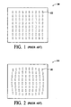
- a typical solid state image sensor array 100 includes photosensitive elements 102, such as photodiodes, that are distributed in a uniform pattern. That is, the distance between any horizontally adjacent photosensitive elements is the same. Similarly, the distance between any vertically adjacent photosensitive elements is the same.
- the image sensor array 100 is not designed to compensate for the distortion of a lens system (not shown), which causes the barrel or pincushion distortions in captured images.
- the image sensor array can be modified to compensate for the distortion of the lens system by positioning the photosensitive elements of the image sensor array in a distribution pattern that takes into account for the distortion of the lens system. (see e.g. EP 0786 814 11 )
- a modified solid state image sensor array 200 that corrects barrel distortions in images is shown.
- the modified image sensor array is configured such that photosensitive elements 102 are distributed in a non-uniform pattern.
- the non-uniform pattern resembles the barrel distortion on images.
- the image signals generated from these photosensitive elements of the image sensor array 200 are then processed in the conventional manner. That is, the image signals are processed as if the signals are from photosensitive elements that are distributed in a uniform pattern. Consequently, the resulting image will have been corrected for the barrel distortion. Similar approach may also be used to correct for pincushion distortions.
- a concern with the use of the modified image sensor array 200 to correct for curvilinear distortions is that the non-uniform distribution pattern of the photosensitive elements 102 may affect the surface area of the photosensitive elements, especially those positioned toward the edges of the image sensor array. Since the density of photosensitive elements needs to be increased toward the edges of the image sensor array, the photosensitive elements near the edges of the image sensor array may have to be smaller in surface size than the photosensitive elements near the center of the image sensor array. Consequently, the efficiency of the image sensor array may be reduced due to the non-uniform distribution of the photosensitive elements.
- modified image sensor array 200 Another concern with the modified image sensor array 200 is that such an image sensor array may be difficult to fabricate.
- the non-uniform distribution of the photosensitive elements may require modification of straight elongated structures of the image sensor array, such as charge coupled device (CCD) channels or electrical connections, into jagged structures with sharp comers to accommodate the non-uniformly distributed photosensitive elements. Consequently, these jagged structures may present a challenge to fabricate the modified image sensor array using a conventional high volume fabrication process.
- CCD charge coupled device
- a solid state image sensor array for correcting curvilinear distortion and method for fabricating the image sensor array utilizes straight line segments that approximate the curvature of the curvilinear distortion to define structures of the image sensor array.
- the use of these straight line segments results in photosensitive elements that are distributed in a non-uniform pattern to compensate for the curvilinear distortion, which may be barrel or pincushion distortion.
- the use of straight line segments increases the efficiency of the photosensitive elements by maximizing the surface area of the photosensitive elements.
- the design of the image sensor array is suitable for conventional high volume fabrication process.
- a solid state image sensor array in accordance with the present invention includes an array of photosensitive elements.
- the photosensitive elements may be photodiodes or other elements that generate charge in response to impinging photons.
- the photosensitive elements are distributed in a non-uniform pattern that compensates for the curvilinear distortion caused by an associated lens system.
- the photosensitive elements are defined by particular areas of the image sensor array. Some of these areas that define the photosensitive elements have a non-perpendicular corner.
- some of the areas of the photosensitive elements are defined by curved line segments that correspond to the curvilinear distortion. In other embodiments, some of the photosensitive elements are defined by straight line segments that form polygonal areas. The polygonal areas may be quadrilateral areas. The orientations of the straight line segments that form the polygonal areas approximate the curvature of the curvilinear distortion.
- the image sensor array may further include elongated structures, such as charge-coupled device channels or conductive strips, having edges that correspond to the curvature of the curvilinear distortion.
- elongated structures such as charge-coupled device channels or conductive strips, having edges that correspond to the curvature of the curvilinear distortion.
- the edges of the elongated structures are defined by curved lines that correspond to the curvature of the curvilinear distortion.
- the edges of the elongated structures are defined by multiple straight line segments that approximate the curvature of the curvilinear distortion.
- a method of fabricating a solid state image sensor array designed to correct for a curvilinear distortion includes the steps of generating an original composite layout of the image sensor array that includes straight line segments that define structures of the image sensor array, transforming the original composite layout into a modified composite layout, which includes warping the straight line segments into curved lines segments that correspond to the curvature of the curvilinear distortion, and forming the structures of the image sensor array using the modified composite layout to fabricate the image sensor array.
- the step of transforming the original composite layout into the modified composite layout includes converting the curved line segments of the structures into replacement straight line segments that approximate the orientations of the curved line segments.
- the step of converting the curved line segments into the replacement straight line segments involves converting some of the curved line segments into single straight line segments, which includes converting curved line segments that define photosensitive elements into sets of straight line segments that form polygonal areas, such as quadrilateral areas.
- the single straight line segments are orientated to conform to the converted curved line segments.
- Some of the polygonal areas formed by the straight line segments have a non-perpendicular corner.
- the step of converting the curved line segments into the replacement straight line segments involves converting some of the curved line segments into multiple straight line segments that substantially trace the converted curved line segments, which includes converting some of the curved line segments that define elongated structures of the image sensor array into sets of multiple straight line segments that trace the converted curved line segments.
- the elongated structures may include charge-coupled device channels or conductive strips.
- Fig. 1 illustrates the layout of a conventional solid state image sensor array having photosensitive elements distributed in a uniform pattern.
- Fig. 2 illustrates the layout of a conventional solid state image sensor array having photosensitive elements distributed in a non-uniform pattern to correct for the curvilinear distortion of an associated camera lens system.
- Fig. 3 illustrates the layout of a charge-coupled device (CCD) image sensor array in accordance with a first exemplary embodiment of the present invention.
- CCD charge-coupled device
- Fig. 4A illustrates a reference image without any distortion.
- Fig. 4B illustrates a comparison image with barrel distortion.
- Fig. 5 illustrates the layout of a CCD image sensor array in accordance with a second exemplary embodiment of the present invention.
- Fig. 6 illustrates the difference between a CCD channel with curved edges that conform to the curvature of the curvilinear distortion and a CCD channel with multiple line segment edges that approximate the curvature of the curvilinear distortion.
- Fig. 7 is process flow diagram of a method for fabricating the CCD image sensor array of Fig. 5 in accordance with the present invention.
- Fig. 8 illustrates the manner in which a CCD channel can be converted from a warped feature defined by curved line segments to an approximated feature defined by multiple straight line segments.
- Fig. 9 illustrates the layout of a complementary metal oxide semiconductor (CMOS) sensor array in accordance with an exemplary embodiment of the present invention.
- CMOS complementary metal oxide semiconductor
- a charge-coupled device (CCD) image sensor array 300 in accordance with a first exemplary embodiment the invention is shown.
- the CCD image sensor array is designed to correct for curvilinear distortion of an associated lens system (not shown).
- the image sensor array includes photosensitive elements 302 that are distributed in a non-uniform pattern to compensate for the curvilinear distortion of the lens system.
- the curvilinear distortion may cause "barrel” distortion, "pincushion” distortion or any other type of spatial distortion in images captured using the associated lens system.
- the image sensor array is illustrated and described herein as being designed to correct for curvilinear distortion that causes barrel distortion in images.
- the design of the CCD image sensor array improves the efficiency of the photosensitive elements by maximizing the surface areas of the photosensitive elements, especially those photosensitive elements that are significantly reduced in size due to the non-uniform distribution of the photosensitive elements.
- the effects of barrel distortion can be shown by comparing a reference image 402 without any distortion to a comparison image 404 with barrel distortion, which are shown in Figs. 4A and 4B.
- the reference image includes dots that are distributed throughout the image.
- the comparison image includes corresponding dots that are also distributed throughout the image. In the reference image, the dots are distributed uniformly throughout the image. That is, the distance between any adjacent dots of the reference image is the same. In the comparison image, the dots are distributed non-uniformly throughout the image. That is, the distance between adjacent dots of the comparison image vary depending on their position in the image. Due to the barrel distortion, the dots near the edges of the comparison image are closer together than the dots near the center of the comparison image.
- the dots of the reference and comparison images can be thought of as image pixels that form the images. An image pixel corresponds to a photosensitive element of the image sensor array that was used to capture the image.
- the CCD image sensor array 300 includes a number of pixel regions 304.
- Each pixel region of the image sensor array includes a photosensitive element 302, or more precisely, a photodiode.
- the photosensitive elements are distributed throughout the image sensor array in a non-uniform pattern, similar to the non-uniform distribution of the dots of the comparison image 404 with barrel distortion in Fig. 4B and the non-uniform photosensitive element distribution of the modified solid state image sensor array 200 of Fig. 2.
- the image sensor array 300 can be used to correct barrel distortions by processing image signals from the photosensitive elements 302 as if the signals are from photosensitive elements that are distributed in a conventional uniform pattern, as illustrated by the photosensitive elements 102 of the image sensor array 100 in Fig. 1.
- Each captured image signal corresponds to an individual image pixel that forms the captured image.
- the resulting image pixels are positioned in a uniform pattern similar to the uniform distribution of the dots of the reference image 404 without any distortion in Fig. 4B, which compensates for the curvilinear distortion of the associated lens system.
- the pixel regions 304 of the CCD image sensor array 300 are defined by curved lines that get closer to each other as these lines approach the edges of the image sensor array.
- the curved lines correspond to the curvature of the curvilinear distortion of the associated lens system. Consequently, the pixel regions of the image sensor array are not rectangular in shape, although the pixel regions in the center of the image sensor array are substantially rectangular. Due to the non-rectangular configuration of the pixel regions, the photosensitive elements of the image sensor array are distributed in the non-uniform pattern. As a result, the photosensitive elements are positioned to correct for the curvilinear distortion of the lens system.
- a section 306 of the image sensor array 300 is shown enlarged to more clearly illustrate the configuration of the individual pixel regions 304 of the image sensor array.
- the enlarged section includes four exemplary pixel regions 304A, 304B, 304C and 304D of the image sensor array that are defined by horizontally orientated curved lines 308, 310 and 312, and vertically orientated curved lines 314, 316 and 318.
- the exemplary pixel regions 304A, 304B, 304C and 304D include photosensitive elements 302A, 302B, 302C and 302D, respectively.
- the CCD image sensor array 300 includes vertically orientated CCD channels that carry accumulated charges from each column of photosensitive elements.
- Two exemplary CCD channels 320A and 320B are shown in the enlarged section 306 of the image sensor array.
- the CCD channels are defined by doped regions, which are formed by doping exposed areas of a semiconductor substrate during fabrication of the image sensor array.
- the CCD channels extend substantially vertical across the image sensor array.
- the vertically orientated edges of the CCD channels are curved in the same manner as the vertically orientated curved lines that define the pixel regions of the image sensor array.
- the vertically orientated edges of the CCD channels correspond to the curvature of the curvilinear distortion.
- each CCD channel is virtually parallel to the nearest vertically orientated curved line that partially defines a column of pixel regions.
- the vertically orientated edges 322 and 324 of the CCD channel 320A are virtually parallel to the vertically orientated curved line 316
- the vertically orientated edges 326 and 328 of the CCD channel 320B are virtually parallel to the vertically orientated curved line 318.
- the CCD image sensor array 300 further includes horizontally orientated electrodes that extend substantially horizontal across the image sensor array.
- Four exemplary horizontally orientated electrodes 330A, 330B, 330C and 330D are shown in the enlarged section 306 of the image sensor array.
- the horizontally orientated electrodes provide appropriate voltages to transfer accumulated charges from a row of photosensitive elements to corresponding vertically orientated CCD channels.
- the horizontally orientated electrodes provide appropriate voltages to vertically transfer the accumulated charges along the CCD channels.
- the vertically and horizontally orientated edges of the electrodes are curved in the same manner as the vertically and horizontally orientated curved lines that define the pixel regions 304 of the image sensor array 300.
- the vertically orientated edges of the electrodes are virtually parallel to the nearest vertically orientated curved line that partially defines a column of pixel regions.
- the horizontally orientated edges of the electrodes are virtually parallel to the nearest horizontally orientated curved line that partially defines a row of pixel regions.
- the vertically orientated edges of the electrodes 330A, 330B, 330C and 330D are virtually parallel to the nearest curved line of the vertically orientated curved lines 314, 316 and 318, while the horizontally orientated edges of the electrodes are virtually parallel to the nearest curved line of the horizontally orientated curved lines 308, 310 and 312.
- the vertically and horizontally orientated edges of the photosensitive elements 302 of the image sensor array 300 are curved in the same manner as the vertically and horizontally orientated curved lines that define the pixel regions 304 of the image sensor array.
- the vertically and horizontally orientated edges of the photosensitive element within each pixel region of the image sensor array are virtually parallel to the vertically and horizontally orientated curved lines that define that pixel region. Consequently, the shape of a photosensitive element within a pixel region is substantially similar to the shape of that pixel region. Since the edges of the photosensitive elements are curved, the surface areas that define the photosensitive elements do not have perpendicular comers.
- the configuration of the photosensitive elements maximizes the surface area of the photosensitive elements, especially the photosensitive elements near the edges of the image sensor array. Thus, the efficiency of the image sensor array is greater than a comparable image sensor array with rectangular photosensitive elements.
- the CCD image sensor array 300 further includes a light shield layer (not shown) that overlies the CCD channels and the electrodes.
- the light shield layer is patterned to expose only the photosensitive elements 302. Thus, the exposed areas of the light shield layer are shaped substantially similar to the photosensitive elements.
- a concern with the CCD image sensor array 300 of Fig. 3 is that the curved edges of the photosensitive elements 302, the CCD channels and the electrodes are difficult to fabricate and thus, the image sensor array is not suitable for conventional high-volume semiconductor fabrication.
- a pattern generator typically uses rectangular shapes to form the patterns of masks. Consequently, masks with curved edges cannot be created using a conventional pattern generator.
- the layout of the CCD image sensor array 300 is not suitable for conventional high-volume fabrication process.
- a CCD image sensor array 500 in accordance with a second exemplary embodiment of the invention is shown.
- the image sensor array 500 includes the same elements as the image sensor array 300 of Fig. 3.
- the image sensor array 500 includes photosensitive elements 502 within pixel regions 504, which are defined by intersecting horizontal and vertical curved lines.
- a section 506 of the image sensor array 500 is shown enlarged to more clearly illustrate the configuration of the individual pixel regions 504 of the image sensor array.
- the enlarged section 506 includes four exemplary pixel regions 504A, 5048, 504C and 504D of the image sensor array 500 that are defined by horizontally orientated curved lines 508, 510 and 512 and vertically orientated curved lines 514, 516 and 518.
- the exemplary pixel regions 504A, 504B, 504C and 504D include photosensitive elements 502A, 502B, 502C and 502D, respectively.
- the CCD image sensor array 500 includes vertically orientated CCD channels and horizontally orientated electrodes, which are illustrated by exemplary CCD channels 520A and 520B and exemplary electrodes 530A, 530B, 530C and 530D.
- the CCD channel 520A is defined by horizontally orientated edges 522 and 524, while the CCD channel 520B is defined by horizontally orientated edges 526 and 528.
- the edges that define the photosensitive elements 502, the vertical CCD channels and the electrodes of the image sensor array 500 are not curved in a continuous fashion. Instead, these edges of the image sensor array 500 approximate corresponding curved lines of the image sensor array 300 using straight line segments.
- the image sensor array 500 is virtually identical to the image sensor array 300, except that the continuous curved edges of the photosensitive elements 302, the vertical CCD channels and the electrodes of the image sensor array 300 of Fig. 3 are replaced with one or more straight line segments, which approximate the corresponding continuous curved edges.
- edges of the photosensitive elements 502, the CCD channels and the electrodes of the image sensor array 500 that are shorter than a predefined length, for example, the width of a standard pixel region, are each replaced with a single straight line segment.
- a predefined length for example, the width of a standard pixel region.
- each of the vertically and horizontally orientated edges of the photosensitive elements 502 is a single straight line segment that approximates the corresponding curved edge in the image sensor array 300 of Fig. 3. Consequently, many of the photosensitive elements 502 are configured as non-rectangular quadrilaterals. Therefore, much of the photosensitive elements 502 have one or more non-perpendicular angles.
- each of the vertically orientated edges of the electrodes of the image sensor array 500 is replaced with a single straight line segment that approximates the corresponding curved edge in the image sensor array 300.
- edges of the image sensor array 500 that are longer than the predefined length, such as the vertically orientated edges of the CCD channels, are each replaced with a number of straight line segments that approximate the corresponding curved edge of the image sensor array 300 of Fig. 3.
- the use of multiple straight line segments to approximate curved edges is illustrate in Fig. 6.
- the curved dotted lines 602 and 604 in Fig. 8 represent vertically orientated edges of a CCD channel of the image sensor array 300.
- the solid lines 606 and 608 in Fig. 8, which are formed by multiple straight line segments, represent edges of a corresponding CCD channel of the image sensor array 500.
- the multiple straight line segments of the solid lines 606 and 608 trace the corresponding curved dotted lines 602 and 604.
- the multiple straight line segments of the solid lines 606 and 608 approximate the curved dotted lines 602 and 604.
- a method for fabricating the CCD image sensor array 500, which is designed to correct for curvilinear distortion of the associated lens system, in accordance with the invention is described with reference to Fig. 7.
- the curvilinear distortion of the associated lens system is characterized so that the image sensor array can be designed to compensate for the distortion.
- a conventional composite layout of the image sensor array is generated as input pattern data using known computer-assisted design (CAD) software.
- the conventional composite layout is a multi-level representation of various structures of the image sensor array to be fabricated, such as the photosensitive elements 502A, 502B, 502C and 502D, the electrodes 530A, 530B, 530C and 530D, and the CCD channels 520A and 520B.
- the structures of the image sensor array are configured as having vertical and horizontal straight line segments.
- the structures of the image sensor array in the conventional composite layout are defined by geometrical configurations having right angle comers. Consequently, the photosensitive elements 502 are rectangularly shaped.
- the photosensitive elements are not distributed in a non-uniform pattern to correct for the curvilinear distortion, as illustrated by the photosensitive elements 102 of the solid state image sensor array 100 in Fig. 1.
- the conventional composite layout is modified to generate a modified composite layout such that the structures of the image sensor array are configured as having straight line segments that are orientated to approximate the curvature of the curvilinear distortion, as illustrated in Fig. 5.
- the modification of the conventional composite layout is achieved by manipulating the input pattern data using appropriate software that utilizes the characterization of the curvilinear distortion to produce the straight line segments.
- the vertical and horizontal straight line segments in the conventional composite layout are warped into curved line segments that correspond to the curvature of the curvilinear distortion. If the curvilinear distortion is associated with barrel distortion, then the vertical and horizontal straight line segments are warped in the same manner as the curved line segments that define the pixel regions 304 in the image sensor array 300 of Fig. 3.
- the curvilinear distortion is associated with another type of distortion
- the vertical and horizontal straight line segments are warped in a manner that correspond to that specific distortion.
- the curved line segments are then converted into one or more straight line segments that approximate the corresponding curved line segments using a pattern generator, which results in a modified composite layout that resembles the image sensor array 500 in Fig. 5.
- the warped features of the composite layout are filled in using a number of appropriately sized rectangles to generate the modified composite layout.
- a vertically orientated CCD channel can be converted from a warped feature 802 defined by curved line segments 804 and 806 to an approximated feature 808 defined by multiple straight line segments 810 and 812.
- the pattern generator performs the conversion by filling in the warped feature 802 with a number of rectangles, e.g., rectangles 816A, 816B, 816C, 816D and 816E.
- the rectangles may overlap with each other as the curved feature is filled in with the rectangles.
- master pattern images in the form of photomasks or reticles are generated using the modified composite layout.
- the edges of structures in the master pattern images are formed by one or more straight line segments.
- various structures of the image sensor array are then formed on a semiconductor wafer in a conventional high-volume fabrication process.
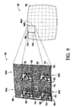
- solid state image sensor arrays described and illustrated herein are CCD sensor arrays having a particular configuration. However, the modifications used to produce the image sensor arrays in accordance with the invention may also be used to modify CCD sensor arrays having different configurations and other types of solid state image sensor arrays, such as complementary metal oxide semiconductor (CMOS) sensor arrays.
- CMOS complementary metal oxide semiconductor
- CMOS sensor array 900 that has been modified in accordance with the invention is shown. Similar to the CCD sensor array 500 of Fig. 5, the CMOS sensor array is configured to compensate for a barrel-type curvilinear distortion. Consequently, the CMOS sensor array includes pixel regions 904 that are distributed in a non-uniform pattern, as illustrated in Fig. 9. An enlarged section 906 of the CMOS sensor array is shown in Fig. 9 to illustrate the configuration of the individual pixel regions 904.
- the enlarged section includes four exemplary pixel regions 904A, 904B, 904C and 904D that are defined by horizontally orientated curved lines 908, 910 and 912 and vertically orientated curved lines 914, 916 and 918.
- the exemplary pixel regions 904A, 904B, 904C and 904D include photosensitive elements 902A, 902B, 902C and 902D.
- the photosensitive elements of the CMOS sensor array are polygonal in shape, as illustrated by the photosensitive elements 902A, 902B, 902C and 902D.
- the exemplary pixel regions 904A, 904B, 904C and 904D includes various metallization strips 920 that provides electrical connections to the photosensitive elements 902A, 902B, 902C and 902D and field-effect transistors (FETs) 922.
- FETs field-effect transistors
- the photosensitive elements and metallization strips are defined by horizontal and vertical straight line segments. Consequently, the conventional photosensitive elements and metallization strips include orthogonal comers.
- the photosensitive elements and metallization strips have been modified in the manner described herein.
- the metallization conductive strips are modified to conform to the curvature of the curvilinear distortion using multiple straight line segments.
- the polygonal photosensitive elements are modified using straight line segments that are rotated to approximate the curvature of the curvilinear distortion, thereby producing many polygonal photosensitive elements with one or more non-perpendicular comers.
Landscapes
- Engineering & Computer Science (AREA)
- Physics & Mathematics (AREA)
- Power Engineering (AREA)
- Multimedia (AREA)
- Signal Processing (AREA)
- Electromagnetism (AREA)
- Condensed Matter Physics & Semiconductors (AREA)
- General Physics & Mathematics (AREA)
- Computer Hardware Design (AREA)
- Microelectronics & Electronic Packaging (AREA)
- Solid State Image Pick-Up Elements (AREA)
- Transforming Light Signals Into Electric Signals (AREA)
Applications Claiming Priority (2)
| Application Number | Priority Date | Filing Date | Title |
|---|---|---|---|
| US62695 | 2002-01-31 | ||
| US10/062,695 US20030141433A1 (en) | 2002-01-31 | 2002-01-31 | Solid state image sensor array for correcting curvilinear distortion of a camera lens system and method for fabricating the image sensor array |
Publications (3)
| Publication Number | Publication Date |
|---|---|
| EP1333498A2 EP1333498A2 (en) | 2003-08-06 |
| EP1333498A3 EP1333498A3 (en) | 2005-05-04 |
| EP1333498B1 true EP1333498B1 (en) | 2007-08-29 |
Family
ID=22044198
Family Applications (1)
| Application Number | Title | Priority Date | Filing Date |
|---|---|---|---|
| EP02021760A Expired - Lifetime EP1333498B1 (en) | 2002-01-31 | 2002-09-25 | Solid state image sensor array for correcting curvilinear distortion of a camera lens system and method for fabricating the image sensor array |
Country Status (5)
| Country | Link |
|---|---|
| US (1) | US20030141433A1 (ja) |
| EP (1) | EP1333498B1 (ja) |
| JP (1) | JP4811625B2 (ja) |
| DE (1) | DE60222086T2 (ja) |
| TW (1) | TW595216B (ja) |
Cited By (1)
| Publication number | Priority date | Publication date | Assignee | Title |
|---|---|---|---|---|
| WO2015019208A1 (en) | 2013-08-08 | 2015-02-12 | Sisvel Technology S.R.L. | Apparatus and method for correcting perspective distortions of images |
Families Citing this family (12)
| Publication number | Priority date | Publication date | Assignee | Title |
|---|---|---|---|---|
| TW576088B (en) * | 2002-07-12 | 2004-02-11 | Veutron Corp | Optical sensor device for receiving light signal |
| WO2009000906A1 (en) | 2007-06-26 | 2008-12-31 | Dublin City University | A method for high precision lens distortion calibration and removal |
| US8077235B2 (en) * | 2008-01-22 | 2011-12-13 | Palo Alto Research Center Incorporated | Addressing of a three-dimensional, curved sensor or display back plane |
| US20090278977A1 (en) * | 2008-05-12 | 2009-11-12 | Jin Li | Method and apparatus providing pre-distorted solid state image sensors for lens distortion compensation |
| US8836805B2 (en) * | 2012-07-17 | 2014-09-16 | Gary Edwin Sutton | Curved sensor system |
| US8248499B2 (en) * | 2009-02-23 | 2012-08-21 | Gary Edwin Sutton | Curvilinear sensor system |
| US8654215B2 (en) | 2009-02-23 | 2014-02-18 | Gary Edwin Sutton | Mobile communicator with curved sensor camera |
| JP2010278295A (ja) * | 2009-05-29 | 2010-12-09 | Nec Toshiba Space Systems Ltd | 撮像装置及び撮像素子の配置方法 |
| EP2742484B1 (en) | 2011-07-25 | 2016-08-31 | Universidade de Coimbra | Method and apparatus for automatic camera calibration using one or more images of a checkerboard pattern |
| CN105245765A (zh) * | 2015-07-20 | 2016-01-13 | 联想(北京)有限公司 | 图像传感阵列及其排布方法、图像采集部件、电子设备 |
| JP7297412B2 (ja) * | 2018-06-13 | 2023-06-26 | キヤノン株式会社 | 画像処理装置、画像処理方法、およびレンズ装置 |
| CN115782180A (zh) * | 2023-01-20 | 2023-03-14 | 杭州爱新凯科技有限公司 | 一种线阵激光打印图像变形矫正方法 |
Family Cites Families (9)
| Publication number | Priority date | Publication date | Assignee | Title |
|---|---|---|---|---|
| JPH01119178A (ja) * | 1987-10-30 | 1989-05-11 | Nikon Corp | 撮像装置 |
| JPH07240877A (ja) * | 1994-02-28 | 1995-09-12 | Mitsubishi Electric Corp | 固体撮像装置 |
| US5489940A (en) * | 1994-12-08 | 1996-02-06 | Motorola, Inc. | Electronic imaging system and sensor for correcting the distortion in a wide-angle lens |
| US5786804A (en) * | 1995-10-06 | 1998-07-28 | Hewlett-Packard Company | Method and system for tracking attitude |
| EP0786815A1 (en) * | 1996-01-26 | 1997-07-30 | Hewlett-Packard Company | Photosensor array with compensation for optical aberrations and illumination nonuniformity |
| JP3461275B2 (ja) * | 1997-12-25 | 2003-10-27 | キヤノン株式会社 | 光電変換装置及びこれを用いたカメラ |
| US6563101B1 (en) * | 2000-01-19 | 2003-05-13 | Barclay J. Tullis | Non-rectilinear sensor arrays for tracking an image |
| JP3728217B2 (ja) * | 2000-04-27 | 2005-12-21 | キヤノン株式会社 | 荷電粒子線露光装置およびデバイス製造方法 |
| US20040012698A1 (en) * | 2001-03-05 | 2004-01-22 | Yasuo Suda | Image pickup model and image pickup device |
-
2002
- 2002-01-31 US US10/062,695 patent/US20030141433A1/en not_active Abandoned
- 2002-09-10 TW TW091120601A patent/TW595216B/zh not_active IP Right Cessation
- 2002-09-25 DE DE60222086T patent/DE60222086T2/de not_active Expired - Lifetime
- 2002-09-25 EP EP02021760A patent/EP1333498B1/en not_active Expired - Lifetime
- 2002-12-16 JP JP2002363626A patent/JP4811625B2/ja not_active Expired - Fee Related
Cited By (1)
| Publication number | Priority date | Publication date | Assignee | Title |
|---|---|---|---|---|
| WO2015019208A1 (en) | 2013-08-08 | 2015-02-12 | Sisvel Technology S.R.L. | Apparatus and method for correcting perspective distortions of images |
Also Published As
| Publication number | Publication date |
|---|---|
| EP1333498A2 (en) | 2003-08-06 |
| US20030141433A1 (en) | 2003-07-31 |
| JP2003229563A (ja) | 2003-08-15 |
| EP1333498A3 (en) | 2005-05-04 |
| DE60222086T2 (de) | 2008-04-30 |
| TW595216B (en) | 2004-06-21 |
| DE60222086D1 (de) | 2007-10-11 |
| JP4811625B2 (ja) | 2011-11-09 |
Similar Documents
| Publication | Publication Date | Title |
|---|---|---|
| EP1333498B1 (en) | Solid state image sensor array for correcting curvilinear distortion of a camera lens system and method for fabricating the image sensor array | |
| US8598640B2 (en) | Solid-state imaging device | |
| US8304354B2 (en) | Methods to avoid laser anneal boundary effect within BSI CMOS image sensor array | |
| US9780131B1 (en) | Image sensor having grid pattern | |
| CN105378926A (zh) | 固态成像器件、固态成像器件的制造方法及电子装置 | |
| JP4431990B2 (ja) | 固体撮像装置 | |
| JP3316106B2 (ja) | 固体撮像装置およびその製造方法 | |
| EP1841202A2 (en) | Solid state imaging apparatus | |
| US8319878B2 (en) | Solid-state imaging device and its production method | |
| JPH07106542A (ja) | 固体撮像素子およびその製造方法 | |
| US7119348B2 (en) | Charged beam writing apparatus and writing method | |
| JPH04192561A (ja) | 固体撮像装置 | |
| CN1941328A (zh) | Cmos图像传感器及其制造方法 | |
| JP3786229B2 (ja) | 画像読み取り装置 | |
| US20240079439A1 (en) | Storage node light shield for pixel of image sensor | |
| JP2016139875A (ja) | 撮像装置 | |
| JP2005252350A (ja) | 固体撮像装置 | |
| JP2006196503A (ja) | 固体撮像素子及びその製造方法 | |
| JPH0774344A (ja) | 電荷転送装置 | |
| JP3467918B2 (ja) | 固体撮像素子の製造方法及び固体撮像素子 | |
| US20100231775A1 (en) | Solid-state imaging element and manufacturing method thereof | |
| JP2003243644A (ja) | 固体撮像装置 | |
| JPH05283663A (ja) | 固体撮像装置 | |
| JP2005064202A (ja) | 固体撮像素子及びその製造方法 | |
| JPH07297378A (ja) | 固体撮像装置およびその製造方法 |
Legal Events
| Date | Code | Title | Description |
|---|---|---|---|
| PUAI | Public reference made under article 153(3) epc to a published international application that has entered the european phase |
Free format text: ORIGINAL CODE: 0009012 |
|
| AK | Designated contracting states |
Designated state(s): AT BE BG CH CY CZ DE DK EE ES FI FR GB GR IE IT LI LU MC NL PT SE SK TR |
|
| AX | Request for extension of the european patent |
Extension state: AL LT LV MK RO SI |
|
| PUAL | Search report despatched |
Free format text: ORIGINAL CODE: 0009013 |
|
| AK | Designated contracting states |
Kind code of ref document: A3 Designated state(s): AT BE BG CH CY CZ DE DK EE ES FI FR GB GR IE IT LI LU MC NL PT SE SK TR |
|
| AX | Request for extension of the european patent |
Extension state: AL LT LV MK RO SI |
|
| 17P | Request for examination filed |
Effective date: 20050829 |
|
| AKX | Designation fees paid |
Designated state(s): DE FR GB |
|
| RAP1 | Party data changed (applicant data changed or rights of an application transferred) |
Owner name: AGILENT TECHNOLOGIES, INC. |
|
| GRAP | Despatch of communication of intention to grant a patent |
Free format text: ORIGINAL CODE: EPIDOSNIGR1 |
|
| GRAS | Grant fee paid |
Free format text: ORIGINAL CODE: EPIDOSNIGR3 |
|
| GRAA | (expected) grant |
Free format text: ORIGINAL CODE: 0009210 |
|
| AK | Designated contracting states |
Kind code of ref document: B1 Designated state(s): DE FR GB |
|
| REG | Reference to a national code |
Ref country code: GB Ref legal event code: FG4D |
|
| REF | Corresponds to: |
Ref document number: 60222086 Country of ref document: DE Date of ref document: 20071011 Kind code of ref document: P |
|
| ET | Fr: translation filed | ||
| PLBE | No opposition filed within time limit |
Free format text: ORIGINAL CODE: 0009261 |
|
| STAA | Information on the status of an ep patent application or granted ep patent |
Free format text: STATUS: NO OPPOSITION FILED WITHIN TIME LIMIT |
|
| 26N | No opposition filed |
Effective date: 20080530 |
|
| REG | Reference to a national code |
Ref country code: GB Ref legal event code: 732E |
|
| REG | Reference to a national code |
Ref country code: FR Ref legal event code: TP |
|
| REG | Reference to a national code |
Ref country code: FR Ref legal event code: RM |
|
| REG | Reference to a national code |
Ref country code: GB Ref legal event code: 732E Free format text: REGISTERED BETWEEN 20101007 AND 20101013 |
|
| PGFP | Annual fee paid to national office [announced via postgrant information from national office to epo] |
Ref country code: FR Payment date: 20110922 Year of fee payment: 10 |
|
| REG | Reference to a national code |
Ref country code: FR Ref legal event code: ST Effective date: 20130531 |
|
| PG25 | Lapsed in a contracting state [announced via postgrant information from national office to epo] |
Ref country code: FR Free format text: LAPSE BECAUSE OF NON-PAYMENT OF DUE FEES Effective date: 20121001 |
|
| PGFP | Annual fee paid to national office [announced via postgrant information from national office to epo] |
Ref country code: GB Payment date: 20160830 Year of fee payment: 15 |
|
| PGFP | Annual fee paid to national office [announced via postgrant information from national office to epo] |
Ref country code: DE Payment date: 20160928 Year of fee payment: 15 |
|
| REG | Reference to a national code |
Ref country code: DE Ref legal event code: R119 Ref document number: 60222086 Country of ref document: DE |
|
| GBPC | Gb: european patent ceased through non-payment of renewal fee |
Effective date: 20170925 |
|
| PG25 | Lapsed in a contracting state [announced via postgrant information from national office to epo] |
Ref country code: DE Free format text: LAPSE BECAUSE OF NON-PAYMENT OF DUE FEES Effective date: 20180404 Ref country code: GB Free format text: LAPSE BECAUSE OF NON-PAYMENT OF DUE FEES Effective date: 20170925 |