EP1327890B1 - Method of optimizing a plurality of tests used in digital integrated circuits - Google Patents
Method of optimizing a plurality of tests used in digital integrated circuits Download PDFInfo
- Publication number
- EP1327890B1 EP1327890B1 EP02258130A EP02258130A EP1327890B1 EP 1327890 B1 EP1327890 B1 EP 1327890B1 EP 02258130 A EP02258130 A EP 02258130A EP 02258130 A EP02258130 A EP 02258130A EP 1327890 B1 EP1327890 B1 EP 1327890B1
- Authority
- EP
- European Patent Office
- Prior art keywords
- vector
- correlation
- tests
- test
- vectors
- Prior art date
- Legal status (The legal status is an assumption and is not a legal conclusion. Google has not performed a legal analysis and makes no representation as to the accuracy of the status listed.)
- Expired - Lifetime
Links
Images

Classifications
-
- G—PHYSICS
- G01—MEASURING; TESTING
- G01R—MEASURING ELECTRIC VARIABLES; MEASURING MAGNETIC VARIABLES
- G01R31/00—Arrangements for testing electric properties; Arrangements for locating electric faults; Arrangements for electrical testing characterised by what is being tested not provided for elsewhere
- G01R31/28—Testing of electronic circuits, e.g. by signal tracer
- G01R31/317—Testing of digital circuits
- G01R31/3181—Functional testing
- G01R31/3183—Generation of test inputs, e.g. test vectors, patterns or sequences
- G01R31/318342—Generation of test inputs, e.g. test vectors, patterns or sequences by preliminary fault modelling, e.g. analysis, simulation
- G01R31/31835—Analysis of test coverage or failure detectability
-
- G—PHYSICS
- G06—COMPUTING OR CALCULATING; COUNTING
- G06F—ELECTRIC DIGITAL DATA PROCESSING
- G06F11/00—Error detection; Error correction; Monitoring
- G06F11/22—Detection or location of defective computer hardware by testing during standby operation or during idle time, e.g. start-up testing
-
- G—PHYSICS
- G06—COMPUTING OR CALCULATING; COUNTING
- G06F—ELECTRIC DIGITAL DATA PROCESSING
- G06F11/00—Error detection; Error correction; Monitoring
- G06F11/22—Detection or location of defective computer hardware by testing during standby operation or during idle time, e.g. start-up testing
- G06F11/2273—Test methods
Definitions
- This invention relates generally to the field of integrated circuit systems, and more specifically to the detection of defects in digital integrated circuits.
- the post-production testing process An important aspect of the manufacture of integrated circuits (IC's) is the post-production testing process.
- the goal of the post-production testing process is to apply test inputs to a device and determine if the device is defective. Preferably, this defect detection process occurs as early point as possible since further integration of faulty components rapidly becomes very expensive. Consider for example, attempting to determine the location of a faulty IC in a personal computer system.
- Functional testing tests the functions present on the IC for correct operation.
- the fault model test determines each type of fault that is likely to occur, and devises tests for these common faults.
- test plan should use the least number of test inputs to cover the most number of defects or defective dice (DD's), and the test plan should be designed so that a test sequence is executed in an efficient fashion.
- Many of the exhaustive, functional, and fault models are based upon RTL and schematics.
- PLMP manufacture process
- RIT's redundant tests and inefficient tests
- Current strategies that reduce the number of RIT's seek to eliminate the execution of redundant tests in the IC testing process using the same exhaustive, functional, and fault model strategies used in IC standardized IC testing.
- Eliminating redundant tests and reordering tests to increase the test efficiency has become an important area of research as the IC test becomes increasingly expensive. In IC testing, tests are generated using simulations and other means. Evaluating the tests is important for increasing test efficiency and reducing test time.
- the present invention seeks to provide improved testing of integrated circuits. According to an aspect of the present invention, there is provided a method as specified in claim 1. According to another aspect of the present invention, there is provided a method as specified in claim 8.
- the preferred embodiments can provide efficient numerical algorithms for analyzing the test redundancy and the test sequence efficiency to meet the need for IC test time reduction techniques.
- the preferred embodiment provides an N 2 algorithm for optimizing IC tests.
- the test optimization refers to minimizing the amount of time spent on RIT's.
- the method uses the IC simulation data or IC production test data.
- the simulation data contains the relation between tests and defects.
- the iC production data reflects the PLMP and gives the relation between tests and DD's. Both of the data can then be processed to detect RIT's in IC tests.
- the test optimization can occur on the defect (fault) level using IC simulation data and the DD level using IC production data.
- the optimization process is the same for both defects (faults) and DD's, so only one approach will be described here.
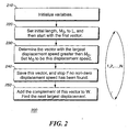
- the test optimization problem may be described as follows: Given N tests in a test sequence and L DD's, each of the N tests detects between 1 and L of the L DD's. And each test takes a certain amount of time to be executed. The first part of the test optimization problem determines the set of tests which takes the minimum number of tests to detect all the L DD's. The second part of the test optimization problem determines the set of tests and the execution sequence of the tests that takes the minimum time to detect all the DD's.
- test optimization problems can be framed in terms of representing N tests as N vectors.
- Each of the N vectors has L components, corresponding to the L DD's.
- V For each of the N tests, we create a correlation vector, V.
- V(i) (v 1 (i), v 2 (i),..., v L (i)), where v j (i) is equal to zero if test i does not detect DD j and is equal to one if test i detects DD j.
- each test can be treated as an event in a correlated event problem.
- the execution time of a test can be treated as the time taken by the corresponding event.
- the list of DD's that a test detects is the correlation vector for the test. Therefore, the test optimization problem is the same as the minimum set optimization and the minimum time optimization problems of correlated events.
- Both parts of the test optimization problem can take on the order of N! operations to determine the optimum set.
- a vector projection technique is used to calculate the correlation between the N correlation vectors. This projection technique requires on the order of N 2 operations to optimize the correlated event problem.
- the following algorithm takes on the order of N 2 operations to determine the minimum set in which each test is represented as a correlation vector:
- the disclosed algorithm for optimizing correlated events is applied to the problem of analyzing redundant tests and reordering tests.
- the problem of analyzing redundant tests and reordering tests is equivalent to analyzing correlated events.
- This description contains three parts: The formulation for correlated events, the algorithm for optimizing the correlated event problem, and the mapping between the correlated event optimization problem and the related test optimization problem.
- N correlated events there is at least one such set of events that their occurrence prevents other events from occurring.
- a minimum set In general, there exists more than one such set of events.
- Such a set of events is called a minimum set.
- the problem of finding the minimum set of events is referred to as a minimum set optimization problem.
- events 1 and 5 are the minimum set. Finding the minimum set of a collection of events is difficult in general because the correlation among events is defined implicitly and the value of N is often large. Therefore, the complexity of the computation for finding a minimum set is very high.
- each of the N events as a binary vector in an L-dimensional correlation space.
- Each of the components of a binary vector is (0,1) valued.
- the binary vectors are called correlation vectors.
- V(i) be the correlation vector associated with event i.
- V(i) (v 1 (i), v 2 (i),..., v L (i))
- v j (i) is the jth component of correlation vector V(i) and is (0,1)-valued.
- I be the unit correlation vector. All the components of the unit correlation vector are one.
- This equation can also be written as
- the correlation vectors determine the correlation among the N events through equation (1) or equation (2).
- the minimum set optimization is to find a set of events so that the value of the variable a in equation (1) or equation (2) reaches it's minimum.
- each event is associated with a time. Let t(i) be the time that event i takes. Then the total time T that events i 1 , i 2 , ... , i a take is
- the minimum time optimization problem is to find a set of events so that the total time T reaches it's minimum. This problem is called minimum time optimization. If all the t(i)'s are equal, then this problem reduces to the minimum set optimization problem.
- P A (B) is the square of the length of the projection of correlation vector B onto correlation vector A.
- P I (W) > 0 and is a decreasing function of k in W. That is, adding a correlation vector to W decreases P I (W).
- the set of events in W will approach a minimum set.
- a set of correlation vectors V(i 1 ), V(i 2 ),..., V(i k )) in the N vectors is chosen such that P I (W) is a minimum.
- P W(i1, i2, ... , ik) (V(i k+1 )) -[P l (W(i 1 , i 2 , ... , i k+1 )) - P l (W(i 1 , i 2 , ... , i k ))]. From this equation, it is seen that P W(i1, i2, ... , ik) (V(i k+1 )) is an amount of the decrement of P I (W) after adding a (k+1)th correlation vector into W. It is possible to treat the value of P W(i1, i2, ...
- the minimum time algorithm and the minimum set algorithm contain two loops related to the number of events, N.
- the number of operations is proportional to N 2 which is much smaller than O(N!).
- bit maps can be used to store the correlation vectors so that less memory is used and bit-wise operations are used to calculate W. The use of bit maps and bit-wise operations also reduce the amount of time required to execute the algorithms.
- the minimum set optimization algorithm can be applied to the determination of how to remove redundant tests and reorder tests in an efficient sequence such that higher efficient tests are executed earlier.
- the minimum time optimization algorithm can be applied to the determination of how to remove redundant tests and the efficient test execution sequence. If we associate N with the number of tests in a given test sequence, and L with the number of DD's, then we can represent the N tests as L-dimensional correlation vectors. With this assignment, it becomes possible to apply the minimum set optimization and minimum time optimization to RIT's.
Landscapes
- Engineering & Computer Science (AREA)
- General Engineering & Computer Science (AREA)
- Theoretical Computer Science (AREA)
- Physics & Mathematics (AREA)
- General Physics & Mathematics (AREA)
- Computer Hardware Design (AREA)
- Quality & Reliability (AREA)
- Tests Of Electronic Circuits (AREA)
- Testing Or Measuring Of Semiconductors Or The Like (AREA)
Applications Claiming Priority (2)
| Application Number | Priority Date | Filing Date | Title |
|---|---|---|---|
| US47344 | 2002-01-15 | ||
| US10/047,344 US6941497B2 (en) | 2002-01-15 | 2002-01-15 | N-squared algorithm for optimizing correlated events |
Publications (3)
| Publication Number | Publication Date |
|---|---|
| EP1327890A2 EP1327890A2 (en) | 2003-07-16 |
| EP1327890A3 EP1327890A3 (en) | 2003-09-03 |
| EP1327890B1 true EP1327890B1 (en) | 2005-06-08 |
Family
ID=21948424
Family Applications (1)
| Application Number | Title | Priority Date | Filing Date |
|---|---|---|---|
| EP02258130A Expired - Lifetime EP1327890B1 (en) | 2002-01-15 | 2002-11-26 | Method of optimizing a plurality of tests used in digital integrated circuits |
Country Status (5)
| Country | Link |
|---|---|
| US (1) | US6941497B2 (enExample) |
| EP (1) | EP1327890B1 (enExample) |
| JP (1) | JP2003232838A (enExample) |
| KR (1) | KR100966010B1 (enExample) |
| DE (1) | DE60204535T2 (enExample) |
Families Citing this family (12)
| Publication number | Priority date | Publication date | Assignee | Title |
|---|---|---|---|---|
| US20040006447A1 (en) * | 2000-06-22 | 2004-01-08 | Jacky Gorin | Methods and apparatus for test process enhancement |
| US7167811B2 (en) * | 2001-05-24 | 2007-01-23 | Test Advantage, Inc. | Methods and apparatus for data analysis |
| US7225107B2 (en) * | 2001-05-24 | 2007-05-29 | Test Advantage, Inc. | Methods and apparatus for data analysis |
| US7395170B2 (en) * | 2001-05-24 | 2008-07-01 | Test Advantage, Inc. | Methods and apparatus for data analysis |
| US7904279B2 (en) * | 2004-04-02 | 2011-03-08 | Test Advantage, Inc. | Methods and apparatus for data analysis |
| JP4849798B2 (ja) * | 2004-12-28 | 2012-01-11 | 富士通株式会社 | 電子機器、記録制御方法及びプログラム |
| TW200724949A (en) * | 2005-08-19 | 2007-07-01 | Koninkl Philips Electronics Nv | Test sequence optimization method and design tool |
| US7596731B1 (en) * | 2006-04-07 | 2009-09-29 | Marvell International Ltd. | Test time reduction algorithm |
| US8180142B2 (en) * | 2008-12-02 | 2012-05-15 | International Business Machines Corporation | Test fail analysis on VLSI chips |
| US8484592B1 (en) | 2012-02-29 | 2013-07-09 | Umm Al-Qura University | Timing verification method for circuits |
| US9401222B1 (en) | 2015-11-23 | 2016-07-26 | International Business Machines Corporation | Determining categories for memory fail conditions |
| KR102782974B1 (ko) | 2019-10-21 | 2025-03-18 | 삼성전자주식회사 | 반도체 회로를 검증하기 위한 최적화된 검증 벡터를 생성하는 전자 장치 및 그 동작 방법 |
Family Cites Families (10)
| Publication number | Priority date | Publication date | Assignee | Title |
|---|---|---|---|---|
| JPH0536802A (ja) * | 1991-07-31 | 1993-02-12 | Hitachi Ltd | 半導体集積回路補修診断方法 |
| JP2785901B2 (ja) * | 1992-03-27 | 1998-08-13 | 松下電器産業株式会社 | 検査系列生成方法および検査系列生成装置 |
| DE69333510T2 (de) | 1992-03-27 | 2005-08-18 | Matsushita Electric Industrial Co., Ltd., Kadoma | Verfahren und Gerät zur Prüfsequenzgenerierung |
| JPH06282462A (ja) * | 1993-03-26 | 1994-10-07 | Toshiba Corp | 半導体試験装置制御プログラムデバッグ方式 |
| US5345450A (en) * | 1993-03-26 | 1994-09-06 | Vlsi Technology, Inc. | Method of compressing and decompressing simulation data for generating a test program for testing a logic device |
| US5935264A (en) | 1997-06-10 | 1999-08-10 | Micron Technology, Inc. | Method and apparatus for determining a set of tests for integrated circuit testing |
| US6070131A (en) * | 1997-09-26 | 2000-05-30 | Micron Technology, Inc. | System for evaluating and reporting semiconductor test processes |
| KR100311013B1 (ko) * | 1998-07-04 | 2001-11-22 | 윤종용 | 테스트시퀀스데이터의압축방법 |
| US6810372B1 (en) * | 1999-12-07 | 2004-10-26 | Hewlett-Packard Development Company, L.P. | Multimodal optimization technique in test generation |
| US6782501B2 (en) * | 2001-01-23 | 2004-08-24 | Cadence Design Systems, Inc. | System for reducing test data volume in the testing of logic products |
-
2002
- 2002-01-15 US US10/047,344 patent/US6941497B2/en not_active Expired - Lifetime
- 2002-11-26 DE DE60204535T patent/DE60204535T2/de not_active Expired - Lifetime
- 2002-11-26 EP EP02258130A patent/EP1327890B1/en not_active Expired - Lifetime
- 2002-12-16 JP JP2002364187A patent/JP2003232838A/ja active Pending
-
2003
- 2003-01-14 KR KR1020030002469A patent/KR100966010B1/ko not_active Expired - Fee Related
Also Published As
| Publication number | Publication date |
|---|---|
| DE60204535D1 (de) | 2005-07-14 |
| KR100966010B1 (ko) | 2010-06-24 |
| EP1327890A3 (en) | 2003-09-03 |
| EP1327890A2 (en) | 2003-07-16 |
| US20030140287A1 (en) | 2003-07-24 |
| DE60204535T2 (de) | 2006-04-27 |
| KR20030061686A (ko) | 2003-07-22 |
| JP2003232838A (ja) | 2003-08-22 |
| US6941497B2 (en) | 2005-09-06 |
Similar Documents
| Publication | Publication Date | Title |
|---|---|---|
| US4862399A (en) | Method for generating efficient testsets for a class of digital circuits | |
| US5377197A (en) | Method for automatically generating test vectors for digital integrated circuits | |
| US6074426A (en) | Method for automatically generating behavioral environment for model checking | |
| US6993470B2 (en) | Method of evaluating test cases in a simulation environment by harvesting | |
| EP1327890B1 (en) | Method of optimizing a plurality of tests used in digital integrated circuits | |
| US7222317B1 (en) | Circuit comparison by information loss matching | |
| CN114398848B (zh) | 一种测试向量生成方法、装置及存储介质 | |
| US20080127009A1 (en) | Method, system and computer program for automated hardware design debugging | |
| Wu et al. | Bridge fault diagnosis using stuck-at fault simulation | |
| US6681357B2 (en) | MISR simulation tool for memory BIST application | |
| Pomeranz et al. | On error correction in macro-based circuits | |
| US7032202B2 (en) | System and method for implementing a flexible top level scan architecture using a partitioning algorithm to balance the scan chains | |
| Riesgo et al. | A fault model for VHDL descriptions at the register transfer level | |
| Chen et al. | Fast node merging with don't cares using logic implications | |
| US7673288B1 (en) | Bypassing execution of a software test using a file cache | |
| US10346557B2 (en) | Increasing compression by reducing padding patterns | |
| WO2008010648A1 (en) | Matching method for multiple stuck-at faults diagnosis | |
| Seuring et al. | A structural approach for space compaction for concurrent checking and BIST | |
| Chang et al. | A new reasoning scheme for efficient redundancy addition and removal | |
| Lin et al. | Speed binning with high-quality structural patterns from functional timing analysis (FTA) | |
| Johnson et al. | A survey of fault simulation, fault grading and test pattern generation techniques with emphasis on the feasibility of VHDL based fault simulation | |
| Wang et al. | A sequential circuit fault simulation by surrogate fault propagation | |
| JPH08180095A (ja) | 遅延故障シミュレーション方法、及び遅延故障解析装置 | |
| Kang et al. | Accurate logic simulation by overcoming the unknown value propagation problem | |
| GB2400677A (en) | Checking an integrated circuit using pre-production simulation and post-production tests |
Legal Events
| Date | Code | Title | Description |
|---|---|---|---|
| PUAI | Public reference made under article 153(3) epc to a published international application that has entered the european phase |
Free format text: ORIGINAL CODE: 0009012 |
|
| AK | Designated contracting states |
Designated state(s): AT BE BG CH CY CZ DE DK EE ES FI FR GB GR IE IT LI LU MC NL PT SE SK TR |
|
| AX | Request for extension of the european patent |
Extension state: AL LT LV MK RO SI |
|
| PUAL | Search report despatched |
Free format text: ORIGINAL CODE: 0009013 |
|
| AK | Designated contracting states |
Kind code of ref document: A3 Designated state(s): AT BE BG CH CY CZ DE DK EE ES FI FR GB GR IE IT LI LU MC NL PT SE SK TR |
|
| AX | Request for extension of the european patent |
Extension state: AL LT LV MK RO SI |
|
| 17P | Request for examination filed |
Effective date: 20040302 |
|
| 17Q | First examination report despatched |
Effective date: 20040408 |
|
| AKX | Designation fees paid |
Designated state(s): DE FR IT |
|
| GRAP | Despatch of communication of intention to grant a patent |
Free format text: ORIGINAL CODE: EPIDOSNIGR1 |
|
| RTI1 | Title (correction) |
Free format text: METHOD OF OPTIMIZING A SEQUENCE OF TESTS USED IN DIGITAL INTEGRATED CIRCUITS |
|
| GRAS | Grant fee paid |
Free format text: ORIGINAL CODE: EPIDOSNIGR3 |
|
| GRAA | (expected) grant |
Free format text: ORIGINAL CODE: 0009210 |
|
| AK | Designated contracting states |
Kind code of ref document: B1 Designated state(s): DE FR IT |
|
| RTI1 | Title (correction) |
Free format text: METHOD OF OPTIMIZING A PLURALITY OF TESTS USED IN DIGITAL INTEGRATED CIRCUITS |
|
| REF | Corresponds to: |
Ref document number: 60204535 Country of ref document: DE Date of ref document: 20050714 Kind code of ref document: P |
|
| ET | Fr: translation filed | ||
| PLBE | No opposition filed within time limit |
Free format text: ORIGINAL CODE: 0009261 |
|
| STAA | Information on the status of an ep patent application or granted ep patent |
Free format text: STATUS: NO OPPOSITION FILED WITHIN TIME LIMIT |
|
| 26N | No opposition filed |
Effective date: 20060309 |
|
| PGFP | Annual fee paid to national office [announced via postgrant information from national office to epo] |
Ref country code: IT Payment date: 20081125 Year of fee payment: 7 |
|
| PGFP | Annual fee paid to national office [announced via postgrant information from national office to epo] |
Ref country code: FR Payment date: 20081112 Year of fee payment: 7 |
|
| PGFP | Annual fee paid to national office [announced via postgrant information from national office to epo] |
Ref country code: DE Payment date: 20091120 Year of fee payment: 8 |
|
| REG | Reference to a national code |
Ref country code: FR Ref legal event code: ST Effective date: 20100730 |
|
| PG25 | Lapsed in a contracting state [announced via postgrant information from national office to epo] |
Ref country code: FR Free format text: LAPSE BECAUSE OF NON-PAYMENT OF DUE FEES Effective date: 20091130 |
|
| PG25 | Lapsed in a contracting state [announced via postgrant information from national office to epo] |
Ref country code: IT Free format text: LAPSE BECAUSE OF NON-PAYMENT OF DUE FEES Effective date: 20091126 |
|
| REG | Reference to a national code |
Ref country code: DE Ref legal event code: R119 Ref document number: 60204535 Country of ref document: DE Effective date: 20110601 Ref country code: DE Ref legal event code: R119 Ref document number: 60204535 Country of ref document: DE Effective date: 20110531 |
|
| PG25 | Lapsed in a contracting state [announced via postgrant information from national office to epo] |
Ref country code: DE Free format text: LAPSE BECAUSE OF NON-PAYMENT OF DUE FEES Effective date: 20110531 |