EP1327705A1 - Method for producing metal mask and metal mask - Google Patents
Method for producing metal mask and metal mask Download PDFInfo
- Publication number
- EP1327705A1 EP1327705A1 EP01967831A EP01967831A EP1327705A1 EP 1327705 A1 EP1327705 A1 EP 1327705A1 EP 01967831 A EP01967831 A EP 01967831A EP 01967831 A EP01967831 A EP 01967831A EP 1327705 A1 EP1327705 A1 EP 1327705A1
- Authority
- EP
- European Patent Office
- Prior art keywords
- film
- mask
- metal
- mask pattern
- electroconductive
- Prior art date
- Legal status (The legal status is an assumption and is not a legal conclusion. Google has not performed a legal analysis and makes no representation as to the accuracy of the status listed.)
- Withdrawn
Links
Images



Classifications
-
- G—PHYSICS
- G03—PHOTOGRAPHY; CINEMATOGRAPHY; ANALOGOUS TECHNIQUES USING WAVES OTHER THAN OPTICAL WAVES; ELECTROGRAPHY; HOLOGRAPHY
- G03F—PHOTOMECHANICAL PRODUCTION OF TEXTURED OR PATTERNED SURFACES, e.g. FOR PRINTING, FOR PROCESSING OF SEMICONDUCTOR DEVICES; MATERIALS THEREFOR; ORIGINALS THEREFOR; APPARATUS SPECIALLY ADAPTED THEREFOR
- G03F1/00—Originals for photomechanical production of textured or patterned surfaces, e.g., masks, photo-masks, reticles; Mask blanks or pellicles therefor; Containers specially adapted therefor; Preparation thereof
- G03F1/68—Preparation processes not covered by groups G03F1/20 - G03F1/50
-
- C—CHEMISTRY; METALLURGY
- C25—ELECTROLYTIC OR ELECTROPHORETIC PROCESSES; APPARATUS THEREFOR
- C25D—PROCESSES FOR THE ELECTROLYTIC OR ELECTROPHORETIC PRODUCTION OF COATINGS; ELECTROFORMING; APPARATUS THEREFOR
- C25D1/00—Electroforming
- C25D1/08—Perforated or foraminous objects, e.g. sieves
-
- G—PHYSICS
- G03—PHOTOGRAPHY; CINEMATOGRAPHY; ANALOGOUS TECHNIQUES USING WAVES OTHER THAN OPTICAL WAVES; ELECTROGRAPHY; HOLOGRAPHY
- G03F—PHOTOMECHANICAL PRODUCTION OF TEXTURED OR PATTERNED SURFACES, e.g. FOR PRINTING, FOR PROCESSING OF SEMICONDUCTOR DEVICES; MATERIALS THEREFOR; ORIGINALS THEREFOR; APPARATUS SPECIALLY ADAPTED THEREFOR
- G03F7/00—Photomechanical, e.g. photolithographic, production of textured or patterned surfaces, e.g. printing surfaces; Materials therefor, e.g. comprising photoresists; Apparatus specially adapted therefor
Definitions
- the present invention relates to a process for manufacturing various types of electronic devices, and more particularly to a preferable method for manufacturing metal masks using a manufacturing method for electroluminescence (EL) devices.
- EL electroluminescence
- a metal mask is used for forming the desired pattern on the metal films of chromium, stainless steel, and so forth.
- the metal mask may be manufactured using the following methods.
- the precision of the mask during exposure and the precision of etching have a significant influence on the pattern precision of the metal mask as the final product. Consequently, in the various steps, it is necessary to control the dimensions of the pattern at a high precision.
- the metal mask is formed on chromium, stainless steel, or other metals with a high linear expansion coefficient. This resulted in a problem where even a small difference in temperature in the metal material leads to a difference in the dimensional precision between the manufactured metal masks, thereby making it difficult to obtain metal masks having the same dimensional precision.
- the metal masks are prone to variations over time in the dimensions of the material that forms the metal mask and in the dimensions of the stainless steel as the feed material for preparing the metal mask.
- a problem was the difficulty in consistently manufacturing metal masks with the same dimensional precision.
- the present invention takes into consideration the above-mentioned problems and is intended to provide a method for manufacturing a metal mask wherein control of the dimensions can be performed easily, and multiple high-precision metal masks can be formed with each having dimensions of the same precision.
- an electroconductive film having a mask pattern is formed on one principle surface of a transparent plate or a transparent film. Then, a photosensitive film is formed on the electroconductive film. Then, with the electroconductive film used as a mask, the photosensitive film is exposed from the side of the transparent plate or transparent film to form a mask pattern in the same shape as that of the mask pattern of the electroconductive film. Then, a metal plating layer is formed on the electroconductive film. The metal plating layer is then separated to form a metal mask.
- a substrate with an electroconductive film formed on one principle surface of a transparent plate or a transparent film is provided. Then, a first resist film is formed on the electroconductive film of the substrate, a first mask pattern is formed on the first resist film, and the electroconductive film is etched with the resist film as a mask. Thereafter, the first resist film is removed, then, a second resist film is formed on the electroconductive film. Then, the second resist film is exposed from the transparent plate or transparent film side with the electroconductive film as a mask to form a second mask pattern on the second resist film. A metal plating layer is then formed by electroplating on the electroconductive film, and the metal plating layer is separated to form a metal mask.
- the second resist film is preferably a dry film.
- the mask pattern formed on the second resist film preferably includes an opening that narrows as the space on the electroconductive film is farther from the electroconductive film.
- a substrate with an electroconductive film formed on one principle surface of a dielectric plate or a transparent plate or a transparent film is provided. Then, a first resist film is formed on the electroconductive film of the substrate, a first mask pattern is formed on the first resist film, and the electroconductive film is etched with the resist film as a mask. Thereafter, the first resist film is removed, then, a metal plating layer is formed by electroplating on the electroconductive film. The metal plating layer is then separated to form a metal mask having a mask pattern in the same shape as that of the first mask pattern.
- the formation of the mask pattern on the first resist film is preferably performed by means of an electron beam exposure method or a laser beam exposure method.
- the formation of the mask pattern on the first resist film is preferably performed using a master mask.
- an electroconductive film having a mask pattern is formed on one principle surface of a transparent plate or a transparent film. Then, a metal plating layer is formed on the electroconductive film, and the metal plating layer is separated to form a metal mask having a mask pattern in the same shape as that of the mask pattern of the electroconductive film.
- an electroconductive film having a predetermined mask pattern is formed on one principle surface of a dielectric plate, a metal plating layer is formed on the electroconductive film, and the metal plating layer is separated to form a metal mask having a mask pattern in the same shape as that of the mask pattern of the electroconductive film.
- the electroconductive film is preferably a metal film having a principle component of chromium.
- the electroconductive film is preferably an ITO film.
- Another mode of the present invention is a metal mask manufactured by a manufacturing method explained above.
- a metal mask which is obtained by separating a metal plating layer formed on an electroconductive film having a predetermined mask pattern formed on a dielectric plate, has a tapered opening that widens from the separated surface toward the opposite side with the widest opening on the side of the separated surface.
- an electroconductive film having a mask pattern is formed on one principle surface of a transparent plate or a transparent film. Then, a photosensitive film is formed on the electroconductive film. Then, the photosensitive film is exposed from the side of the transparent plate or transparent film with the electroconductive film as a mask to form on the photosensitive film a mask pattern in the same shape as that of the mask pattern of the electroconductive film. In this way, the photosensitive film can be formed on an area on the transparent plate or transparent film where there is no electroconductive film. Therefore, it is easy to select a material having a low coefficient of thermal expansion, such as glass, for the transparent plate or transparent film so as to eliminate changes over time in the dimensions of the mask pattern. In this way, it is easy to control the dimensions of the mask pattern in the process of manufacturing the metal mask.
- a metal plating layer is formed on the electroconductive film. By separating the metal plating layer, it is easy to obtain the metal mask having a pattern in the same shape as that of the mask pattern formed on the photosensitive film.
- an electroconductive film having a mask pattern is formed on one principle surface of a dielectric plate. Then, a metal plating layer having a mask pattern in the same shape as that of the mask pattern of the electroconductive film can be formed on the electroconductive film. This metal plating layer is then separated to form a metal mask. In this way, a material having a low coefficient of thermal expansion, such as glass or ceramic, can be used for the dielectric plate. It becomes easy to control the dimensions of the mask pattern in the process of manufacturing the metal mask. Also, according to this method, the process is simplified so that the manufacturing cost can be reduced.
- the side of the opening in the metal mask has a tapered shape
- the precision of the mask pattern can be improved.
- the metal mask is shaped so that the opening is smallest on the side close to the electroconductive film, the mask pattern becomes precisely the same as the electroconductive film.
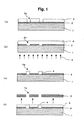
- an electroconductive film for example, a Cr (chromium) film (electroconductive film) 2 with a thickness of 0.1 ⁇ m, is formed by means of vapor deposition or sputtering on the surface of a glass plate 1 (one principal surface). Then, by a means of a spin coating method or the like, a photosensitive material (first resist film) 3 with a thickness of preferably about 0.7 ⁇ m is formed on the Cr film 2.
- a mask pattern 3a is formed directly on photosensitive material 3.
- Cr film 2 is etched.
- a mask pattern 2a corresponding to and preferably in the same shape as that of the mask pattern 3a is formed on the Cr film 2.
- the photosensitive material 3 is separated or removed. Any commonly known process can be conveniently selected for use in this process. For example, in the above-mentioned electron beam exposure method or the laser beam exposure method, a predetermined area on photosensitive material 3 is scanned by the electron beam or laser beam to expose the area. Furthermore, using a master mask, light may be applied only to a predetermined area to expose the photosensitive material 3.
- a preferably 50- ⁇ m-thick dry film 4 is laminated (formed).
- dry film 4 is exposed by a light 5 applied from the glass plate 1 side.
- a mask pattern 4a in the same shape as that of mask pattern 2a is formed on dry film 4.
- a metal plating layer 6 is formed from Ni, Ni-Co alloy, Ni-W alloy, or the like, by means of electroplating.
- the thickness of the metal plating layer 6 is approximately 30 ⁇ m to 50 ⁇ m.
- the metal plating layer 6 is separated, forming a metal mask 7 having a mask pattern 7a in the same shape as that of mask pattern 4a.
- Cr film 2 having mask pattern 2a is formed on the surface of glass plate 1.
- dry film 4 is laminated, and dry film 4 is exposed by light 5 applied from the glass plate 1 side with Cr film 2 as a mask, forming mask pattern 4a corresponding to and preferably in the same shape as that of mask pattern 2a on dry film 4.
- Glass plate 1 acts as the base (wall) of Cr film 2, thereby eliminating the variation over time in the dimensions of the mask pattern. As a result, it is easy to control the dimensions of the mask pattern in the manufacturing process of the metal mask.
- the coefficient of thermal expansion of the glass plate 1 is 1 ⁇ m/°C, which is approximately 1/8 that of stainless steel.
- soda glass is preferable because of its low cost.
- quartz glass is expensive, its advantages include a low coefficient of thermal expansion, excellent light transmission, and scratch resistance.
- metal plating layer 6 is formed by electroplating on Cr film 2, followed by separation of the metal plating layer 6, it is easy to obtain metal mask 7 having mask pattern 7a in the same shape as that of mask pattern 4a.
- a surface treatment (S11) is performed to remove contamination remaining on the surface, such as residue of the metal plating layer 6.
- This surface treatment is performed, for example, by placing the surface in contact with a 20% solution of nitric acid (HNO 3 ) for five minutes in a scrubber.
- the surface is washed in a water shower (S12). In this washing, for example, a 30-second shower is performed twice in a washer.
- a drying process S13
- This drying is performed, for example, by a dryer, by blowing 60°C air for five minutes.
- preheating (S14) is performed. This preheating is performed, for example, by maintaining a temperature of 45°C for five minutes in a chamber.
- dry film (dry film photoresist) 4 is laminated (S15) on the Cr film 2.
- the lamination of dry film is performed, for example, at 100°C by a dry film laminator.
- the thickness of the dry film 4 is approximately 50 ⁇ m.
- an exposure is performed from the back side with respect to the dry film 4.
- the dry film 4 is exposed with Cr film 2 as a mask by applying a predetermined light (80 mJ energy) from the back side of glass plate 1.
- the exposed dry film 4 is developed and the unexposed portions are removed (S17).
- This development is performed, for example, by placing the surface in contact with a 1% solution of sodium carbonate (Na 2 CO 3 ) for 40 seconds.
- the Cr film 2 is exposed and the dry film 4 remains on the other portions.
- the Cr film 2 has a thickness of approximately 0.1 ⁇ m and the dry film 4 has a thickness of approximately 50 ⁇ m so that a wall of the dry film 4 is formed in the periphery of the Cr film 2.
- the entire body is dried (S18) using a dryer. Drying is performed, for example, at 40°C for five minutes. Then, the portion of dry film 4 remaining after drying is checked under a microscope (S19) to determine whether it is appropriate or not. If this check is failed, the dry film 4 is removed (S20) and the process returns to S11.
- the wall of the dry film 4 can be used to form the metal plating layer 6 and in a precise shape.
- the Ni metal plating layer 6 is separated (S23) as a shadow mask (metal mask) from Cr film 2.
- the glass plate 1 having Cr film 2 with the metal mask separated has the dry film 4 removed through a chemical washing (S24) and the process returns to S11.
- the metal mask obtained in S23 is washed in water (S25) in a washer and dried (S26) with a dryer, then various measurements are conducted (S27) using measuring equipment.
- the area on the dry film 4 is preferable to form the area on the dry film 4 to be exposed so that it widens gradually by the light applied from the back side of glass plate 1 by moving the glass plate 1. Namely, if the applied light does not comprise parallel rays, by moving the glass plate 1, some of the applied light reaches the rear side of Cr film 2 to widen the exposed area. Also, a similar exposure can be performed by setting the focus of the applied light in the vicinity of Cr film 2 so that the exposed area subsequently widens. Furthermore, on the back side of the glass plate 1, a diffraction plate or a scattering plate for the applied light may be provided to transform the parallel rays to scattered light oriented in various directions for the exposure. This also allows the light passing the opening of Cr film 2 to diverge from the opening and expose the dry film 4.
- an irregular reflection plate 10 on the side opposite the glass plate 1 of the dry film 4 so that the reflected light by the irregular reflection plate (diffusion board) 10 shines on the dry film 4. Namely, through this configuration, light initially passes dry film 4, is reflected by the irregular reflection plate 10, and again shines toward the glass plate 1. Therefore, adding a distance from the glass plate 1 widens the exposed area.
- the metal plating layer 6 formed by electroplating has tapered sides, which are widest in area on the Cr film 2 and smaller in area toward the top.
- the metal mask 7 formed from the separated metal plating layer 6 is shown in Fig. 4(b), and the smallest part of the opening has the same shape as that of Cr film 2 from where the opening increases in size in the direction of thickness (toward the top in the figure).
- this metal mask defines the smallest part of the opening, which has the same shape as that of the Cr film 2. Therefore, a metal mask having extremely high precision can be obtained.
- this metal mask when used as a vapor deposition mask, an appropriate vapor deposition can be performed. Namely, as EL panels increase in size, the plate for vapor deposition also increases in size. If the opening in the metal mask is straight while performing vapor deposition on such a large plate, a difference in the vapor deposited amount develops between the periphery and the center. However, by tapering the opening of the metal mask, it becomes possible for vapor deposition of material from a diagonal direction at the periphery for a uniform vapor deposited amount. Vapor deposition is performed with the metal mask with the small side of the opening on the plate side. In this way, the area on which vapor deposition is performed can be maintained with accuracy.
- S24 may be performed before the process of separating the metal mask in S23. Namely, as shown in Fig. 5, after electroplating is performed in S22, the dry film 4 is removed (S24). Then, after the dry film 4 has been removed, the metal mask 7 is separated (S23). Then, the glass plate 1 is returned to the surface treatment of S11. In this case, chemicals that do not affect the metal mask 7 are used in S24.
- the photosensitive material (first resist film) 3 with a thickness of 0.7 ⁇ m is formed on the Cr film 2 with a thickness of 0.1 ⁇ m.
- mask pattern 3a is formed directly on photosensitive material 3.
- the photosensitive material 3 used as a mask Cr 2 film is etched.
- mask pattern 2a corresponding to and preferably in the same shape as that of the mask pattern 3a is formed on the Cr film 2. Thereafter, photosensitive material 3 is separated (removed).
- a metal plating layer 11 is formed on the Cr film 2 by means of electroplating.
- the metal plating layer 11 is formed from Ni, Ni-Co alloy, Ni-W alloy, or the like, and a mask pattern 11a is formed in the same shape as that of the mask pattern 2a.
- the metal plating layer 11 is separated from Cr film 2 to form a metal mask 12 having a mask pattern 12a in the same shape as that of mask pattern 2a.
- the metal plating layer 11 is formed by electroplating on the Cr film 2, after which the metal plating layer 11 is separated from the Cr film 2 so as to enable the dimensions of the mask pattern to be easily controlled in the manufacturing process of the metal mask. Furthermore, since the process is simplified, the manufacturing cost can be reduced.
- the second embodiment does not have processes for lamination, exposure, development, and so forth for dry film 4. Therefore, compared to Fig. 2, the processes S14-S20 are omitted and the process for S24 does not exist. The remaining processes are performed in general with conditions identical to those of the first embodiment.
- the electroplating of S22 is performed without dry film 4. Therefore, although the metal plating layer 11 is formed on Cr film 2, it also extends on the side of Cr film 2 as shown in Fig. 8. Therefore, the shape of the metal mask obtained in S23 is not exactly the same as that of the Cr film 2. Therefore, when forming the Cr film 2 in the second embodiment, it is preferable to set the dimensions while taking into consideration that the opening will become smaller from the electroplating.
- the mask pattern 4a to be the guide for the metal plating layer 6 was formed using the dry film 4. Instead of this, a wet resist can also be used. This process will be described with reference to Figs. 9(a)-9(d).
- the Cr film 2 with a thickness of 0.1 ⁇ m, for example, is formed on the surface of the glass plate 1.
- the photosensitive material 3 with a thickness of 0.7 ⁇ m, for example, is formed on the Cr film 2.
- mask pattern 3a is directly formed on the photosensitive material 3.
- the Cr film 2 is etched with the photosensitive material 3 as a mask, and as shown in Fig. 9(b), the mask pattern 2a having the same shape as that of the mask pattern 3a is formed on the Cr film 2.
- a second photosensitive material 8 is formed on top of the photosensitive material 3.
- the second photosensitive material 8 is a liquid and also reaches inside the opening of mask patterns 2a, 3a. Then, in this state, exposure is performed from the back side of the glass plate 1. In this way, the second photosensitive material 8 is exposed so as to correspond to the mask pattern 2a on the Cr film 2.
- the second photosensitive material 8 is etched at the unexposed portion. Furthermore, the photosensitive material 3 is etched. Therefore, by means of dry etching, as shown in Fig. 9(c), the portion exposed on the second photosensitive material forms mask pattern 8a.
- the metal mask can be obtained by using a wet photosensitive material without using dry film.
- the metal mask obtained in the above-mentioned manner is preferably used as a vapor deposition mask for EL panels.
- the EL panel has an EL element at every picture element on the glass plate.
- the EL element has an electron transport layer, an emissive layer, and a hole transport layer between a cathode and an anode.
- the active-type EL panel has a thin-film transistor (TFT) corresponding to each EL element to control light emission at each EL element.
- TFT thin-film transistor
- the necessary material layers are laminated in sequence in a predetermined pattern. Then, since a higher definition display is possible with smaller picture elements, the metal mask of the present invention is preferably used as a mask for the material lamination.
- the metal mask of the present invention is preferably a vapor deposition mask for EL panels.
- the glass plate 1 was used in the method for manufacturing a metal mask in the first and second embodiments.
- the glass plate 1 is only for forming a film of Cr or other electroconductive material, and in addition to glass plate 1, it is also possible to use a heat-resistant resin, heat-resistant resin film, or the like.
- a non-transparent plate instead of the glass plate 1.
- a ceramic plate or the like may be used.
- a master mask can be used to expose the photosensitive material to form mask pattern 3a on the photosensitive material 3.
- Cr film 2 and photosensitive material 3 are formed in sequence on the surface of glass plate 1.
- a substrate with Cr film 2 can be first formed on the surface of glass plate 1, and the photosensitive material 3 can be formed on Cr film 2 of this substrate.
- the film instead of Cr film 2, the film can be a Cr-based alloy having a principle component of chromium or an ITO film.
- dry film 4 is used.
- the dry film 4 may be made of any photosensitive material, such as liquid resist, or other liquid photosensitive resin.
- any type of metal that can be formed by electroplating can be used as the metal for forming metal plating layers 6, 11, such as Ta (tantalum), Mo (molybdenum), W (tungsten), or the like.
- electroplating is used in the aforementioned embodiments.
- electroless plating can be used.
- an electroconductive film having a mask pattern is formed on one principle surface of a transparent plate or a transparent film. Then, a photosensitive film is formed on the electroconductive film. Then, with the electroconductive film used as a mask, the photosensitive film is exposed from the side of the transparent plate or transparent film to form a mask pattern in the same shape as that of the mask pattern on the photosensitive film. In this way, a photosensitive film can be formed on an area on the transparent plate or transparent film where there is no electroconductive film. Therefore, it is easy to select a material having a low coefficient of thermal expansion, such as glass, for the transparent plate or transparent film so as to eliminate changes over time in the dimensions of the mask pattern. In this way, it is easy to control the dimensions of the mask pattern in the process of manufacturing the metal mask.
- a metal plating layer is formed on the electroconductive film. By separating the metal plating layer, it is easy to obtain the metal mask having a pattern in the same shape as that of the mask pattern formed on the photosensitive film.
- an electroconductive film having a mask pattern is formed on one principle surface of a dielectric plate. Then, a metal plating layer having a mask pattern in the same shape as that of the mask pattern can be formed on the electroconductive film. This metal plating layer is then separated to form a metal mask. In this way, a material having a low coefficient of thermal expansion, such as glass or ceramic, can be used for the dielectric plate. It becomes easy to control the dimensions of the mask pattern in the process of manufacturing the metal mask. Also, according to this method, the process is simplified so that the manufacturing cost can be reduced.
- the side of the opening in the metal mask has a tapered shape
- the precision of the mask pattern can be improved.
- the metal mask is shaped so that the opening is smallest on the side close to the electroconductive film, the mask pattern becomes precisely the same as the electroconductive film.
- dimensional control in the manufacturing process is easy so that multiple high-precision masks can be manufactured at the same precision and the manufacturing cost can be reduced.
Landscapes
- Chemical & Material Sciences (AREA)
- Engineering & Computer Science (AREA)
- Chemical Kinetics & Catalysis (AREA)
- Electrochemistry (AREA)
- Materials Engineering (AREA)
- Metallurgy (AREA)
- Organic Chemistry (AREA)
- Physics & Mathematics (AREA)
- General Physics & Mathematics (AREA)
- Physical Vapour Deposition (AREA)
- Electroluminescent Light Sources (AREA)
Abstract
A method for manufacturing a metal mask that
facilitates easy dimensional control in the manufacturing
process and can manufacture multiple metal masks having high
and consistent precision.
A Cr film 2 having a mask pattern 2a is formed on the
surface of a glass plate 1, a dry film 4 is formed on the Cr
film 2, the dry film 4 is exposed from the glass plate 1
side with the Cr film 2 as a mask, a mask pattern 4a having
the same shape as that of the mask pattern 2a is formed on
the dry film 4, and a metal plating layer 6 is formed on the
Cr film 2. The metal plating layer 6 is separated to form a
metal mask 7.
Description
The present invention relates to a process for
manufacturing various types of electronic devices, and more
particularly to a preferable method for manufacturing metal
masks using a manufacturing method for electroluminescence
(EL) devices.
In order to form vapor deposit films of various metals
in the conventional process for manufacturing
electroluminescence (EL) elements and other electronic
devices, a metal mask is used for forming the desired
pattern on the metal films of chromium, stainless steel, and
so forth.
The metal mask may be manufactured using the following
methods.
However, for the conventional methods for
manufacturing metal masks, the precision of the mask during
exposure and the precision of etching have a significant
influence on the pattern precision of the metal mask as the
final product. Consequently, in the various steps, it is
necessary to control the dimensions of the pattern at a high
precision. Moreover, in the conventional methods, the metal
mask is formed on chromium, stainless steel, or other metals
with a high linear expansion coefficient. This resulted in a
problem where even a small difference in temperature in the
metal material leads to a difference in the dimensional
precision between the manufactured metal masks, thereby
making it difficult to obtain metal masks having the same
dimensional precision.
Also, the metal masks are prone to variations over
time in the dimensions of the material that forms the metal
mask and in the dimensions of the stainless steel as the
feed material for preparing the metal mask. Thus, when many
metal masks having high-precision dimensions and small
variations in the dimensions are required, a problem was the
difficulty in consistently manufacturing metal masks with
the same dimensional precision.
For example, when multiple metal masks with the same
dimensional precision in the mask pattern are to be
manufactured, it is possible to form the metal masks with
high precision having little variation at the beginning.
However, as the manufacturing progresses over time,
variations occur in the dimensions, so that the dimensional
precision decreases gradually. Finally, not only does the
dimensional precision degrade, but also the variations in
the dimensions becomes larger. Consequently, it is difficult
to obtain multiple metal masks with high precision and
little variation.
The present invention takes into consideration the
above-mentioned problems and is intended to provide a method
for manufacturing a metal mask wherein control of the
dimensions can be performed easily, and multiple high-precision
metal masks can be formed with each having
dimensions of the same precision.
In one mode of the present invention, an
electroconductive film having a mask pattern is formed on
one principle surface of a transparent plate or a
transparent film. Then, a photosensitive film is formed on
the electroconductive film. Then, with the electroconductive
film used as a mask, the photosensitive film is exposed from
the side of the transparent plate or transparent film to
form a mask pattern in the same shape as that of the mask
pattern of the electroconductive film. Then, a metal plating
layer is formed on the electroconductive film. The metal
plating layer is then separated to form a metal mask.
In another mode of the present invention, a substrate
with an electroconductive film formed on one principle
surface of a transparent plate or a transparent film is
provided. Then, a first resist film is formed on the
electroconductive film of the substrate, a first mask
pattern is formed on the first resist film, and the
electroconductive film is etched with the resist film as a
mask. Thereafter, the first resist film is removed, then, a
second resist film is formed on the electroconductive film.
Then, the second resist film is exposed from the transparent
plate or transparent film side with the electroconductive
film as a mask to form a second mask pattern on the second
resist film. A metal plating layer is then formed by
electroplating on the electroconductive film, and the metal
plating layer is separated to form a metal mask.
Also, the second resist film is preferably a dry film.
Also, the mask pattern formed on the second resist
film preferably includes an opening that narrows as the
space on the electroconductive film is farther from the
electroconductive film.
Also, in another mode of the present invention, a
substrate with an electroconductive film formed on one
principle surface of a dielectric plate or a transparent
plate or a transparent film is provided. Then, a first
resist film is formed on the electroconductive film of the
substrate, a first mask pattern is formed on the first
resist film, and the electroconductive film is etched with
the resist film as a mask. Thereafter, the first resist film
is removed, then, a metal plating layer is formed by
electroplating on the electroconductive film. The metal
plating layer is then separated to form a metal mask having
a mask pattern in the same shape as that of the first mask
pattern.
Also, the formation of the mask pattern on the first
resist film is preferably performed by means of an electron
beam exposure method or a laser beam exposure method.
Also, the formation of the mask pattern on the first
resist film is preferably performed using a master mask.
Also, in another mode of the present invention, an
electroconductive film having a mask pattern is formed on
one principle surface of a transparent plate or a
transparent film. Then, a metal plating layer is formed on
the electroconductive film, and the metal plating layer is
separated to form a metal mask having a mask pattern in the
same shape as that of the mask pattern of the
electroconductive film.
Also, in another mode of the present invention, an
electroconductive film having a predetermined mask pattern
is formed on one principle surface of a dielectric plate, a
metal plating layer is formed on the electroconductive film,
and the metal plating layer is separated to form a metal
mask having a mask pattern in the same shape as that of the
mask pattern of the electroconductive film.
Also, the electroconductive film is preferably a metal
film having a principle component of chromium.
Also, the electroconductive film is preferably an ITO
film.
Also, another mode of the present invention is a metal
mask manufactured by a manufacturing method explained above.
Also, in another mode of the present invention, a
metal mask, which is obtained by separating a metal plating
layer formed on an electroconductive film having a
predetermined mask pattern formed on a dielectric plate, has
a tapered opening that widens from the separated surface
toward the opposite side with the widest opening on the side
of the separated surface.
According to the present invention, an
electroconductive film having a mask pattern is formed on
one principle surface of a transparent plate or a
transparent film. Then, a photosensitive film is formed on
the electroconductive film. Then, the photosensitive film is
exposed from the side of the transparent plate or
transparent film with the electroconductive film as a mask
to form on the photosensitive film a mask pattern in the
same shape as that of the mask pattern of the
electroconductive film. In this way, the photosensitive film
can be formed on an area on the transparent plate or
transparent film where there is no electroconductive film.
Therefore, it is easy to select a material having a low
coefficient of thermal expansion, such as glass, for the
transparent plate or transparent film so as to eliminate
changes over time in the dimensions of the mask pattern. In
this way, it is easy to control the dimensions of the mask
pattern in the process of manufacturing the metal mask.
Also, with the photosensitive film used as a mask, a
metal plating layer is formed on the electroconductive film.
By separating the metal plating layer, it is easy to obtain
the metal mask having a pattern in the same shape as that of
the mask pattern formed on the photosensitive film.
Also, by repeating the step of forming the metal
plating layer on the electroconductive film and the step of
separating the metal plating layer, it is possible to form
multiple high-precision metal masks at the same precision.
Also, according to the present invention, an
electroconductive film having a mask pattern is formed on
one principle surface of a dielectric plate. Then, a metal
plating layer having a mask pattern in the same shape as
that of the mask pattern of the electroconductive film can
be formed on the electroconductive film. This metal plating
layer is then separated to form a metal mask. In this way, a
material having a low coefficient of thermal expansion, such
as glass or ceramic, can be used for the dielectric plate.
It becomes easy to control the dimensions of the mask
pattern in the process of manufacturing the metal mask.
Also, according to this method, the process is simplified so
that the manufacturing cost can be reduced.
Also, because the side of the opening in the metal
mask has a tapered shape, the precision of the mask pattern
can be improved. In particular, because the metal mask is
shaped so that the opening is smallest on the side close to
the electroconductive film, the mask pattern becomes
precisely the same as the electroconductive film.
Also, by shaping the photosensitive film into a
tapered shape, it becomes easy to obtain a metal mask having
a tapered opening.
Embodiments of the manufacturing method for metal
masks according to the present invention will be described
with reference to the drawings.
The manufacturing method for vapor deposited metal
masks for EL devices of the first embodiment according to
the present invention will be described with reference to
Fig. 1.
First, as shown in Fig. 1(a), an electroconductive
film, for example, a Cr (chromium) film (electroconductive
film) 2 with a thickness of 0.1 µm, is formed by means of
vapor deposition or sputtering on the surface of a glass
plate 1 (one principal surface). Then, by a means of a spin
coating method or the like, a photosensitive material (first
resist film) 3 with a thickness of preferably about 0.7 µm
is formed on the Cr film 2.
Then, by means of an electron beam exposure method,
laser beam exposure method; or the like, a mask pattern 3a
is formed directly on photosensitive material 3. Then, with
the photosensitive material 3 used as a mask, Cr film 2 is
etched. As shown in Fig. 1(b), a mask pattern 2a
corresponding to and preferably in the same shape as that of
the mask pattern 3a is formed on the Cr film 2. Thereafter,
the photosensitive material 3 is separated or removed. Any
commonly known process can be conveniently selected for use
in this process. For example, in the above-mentioned
electron beam exposure method or the laser beam exposure
method, a predetermined area on photosensitive material 3 is
scanned by the electron beam or laser beam to expose the
area. Furthermore, using a master mask, light may be applied
only to a predetermined area to expose the photosensitive
material 3.
Then, on the Cr film 2, a preferably 50-µm-thick dry
film 4 is laminated (formed). With the Cr film 2 used as a
mask, dry film 4 is exposed by a light 5 applied from the
glass plate 1 side. In this way, as shown in Fig. 1(c), a
mask pattern 4a in the same shape as that of mask pattern 2a
is formed on dry film 4.
Then, as shown in Fig. 1(d), after pretreatment of Cr
film 2, a metal plating layer 6 is formed from Ni, Ni-Co
alloy, Ni-W alloy, or the like, by means of electroplating.
The thickness of the metal plating layer 6 is approximately
30 µm to 50 µm. Thereafter, the metal plating layer 6 is
separated, forming a metal mask 7 having a mask pattern 7a
in the same shape as that of mask pattern 4a.
Also, by repeating the steps shown in Figs. 1(c)-1(d),
multiple high precision metal masks 7 can be made with each
having the same precision.
By means of the method for manufacturing a metal mask
in this embodiment, Cr film 2 having mask pattern 2a is
formed on the surface of glass plate 1. On the Cr film 2,
dry film 4 is laminated, and dry film 4 is exposed by light
5 applied from the glass plate 1 side with Cr film 2 as a
mask, forming mask pattern 4a corresponding to and
preferably in the same shape as that of mask pattern 2a on
dry film 4. Glass plate 1 acts as the base (wall) of Cr film
2, thereby eliminating the variation over time in the
dimensions of the mask pattern. As a result, it is easy to
control the dimensions of the mask pattern in the
manufacturing process of the metal mask.
The coefficient of thermal expansion of the glass
plate 1 is 1 µm/°C, which is approximately 1/8 that of
stainless steel. By using the glass plate 1, it is possible
to suppress deterioration of precision due to heat. Also,
although various types of glass materials can be used, soda
glass is preferable because of its low cost. On the other
hand, although quartz glass is expensive, its advantages
include a low coefficient of thermal expansion, excellent
light transmission, and scratch resistance.
Also, as metal plating layer 6 is formed by
electroplating on Cr film 2, followed by separation of the
metal plating layer 6, it is easy to obtain metal mask 7
having mask pattern 7a in the same shape as that of mask
pattern 4a.
By performing this process repeatedly, it is possible
to form multiple high-precision metal masks 7 with each
having the same precision.
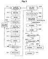
Next, the steps for manufacturing the metal mask using
the glass plate 1 having Cr film 2 will be described in
detail with reference to Fig. 2.
First, for the glass plate 1 on which Cr film 2 is
formed, a surface treatment (S11) is performed to remove
contamination remaining on the surface, such as residue of
the metal plating layer 6. This surface treatment is
performed, for example, by placing the surface in contact
with a 20% solution of nitric acid (HNO3) for five minutes in
a scrubber. Next, the surface is washed in a water shower
(S12). In this washing, for example, a 30-second shower is
performed twice in a washer. After washing, a drying process
(S13) is performed. This drying is performed, for example,
by a dryer, by blowing 60°C air for five minutes. After
completion of this drying process, preheating (S14) is
performed. This preheating is performed, for example, by
maintaining a temperature of 45°C for five minutes in a
chamber.
When washing and preheating are completed in this
manner for the glass plate 1 having Cr film 2, dry film (dry
film photoresist) 4 is laminated (S15) on the Cr film 2. The
lamination of dry film is performed, for example, at 100°C by
a dry film laminator. The thickness of the dry film 4 is
approximately 50 µm.
Next, an exposure (S16) is performed from the back
side with respect to the dry film 4. Namely, the dry film 4
is exposed with Cr film 2 as a mask by applying a
predetermined light (80 mJ energy) from the back side of
glass plate 1. Then, the exposed dry film 4 is developed and
the unexposed portions are removed (S17). This development
is performed, for example, by placing the surface in contact
with a 1% solution of sodium carbonate (Na2CO3) for 40
seconds. By performing development in this manner, the Cr
film 2 is exposed and the dry film 4 remains on the other
portions. Namely, the Cr film 2 has a thickness of
approximately 0.1 µm and the dry film 4 has a thickness of
approximately 50 µm so that a wall of the dry film 4 is
formed in the periphery of the Cr film 2.
Next, the entire body is dried (S18) using a dryer.
Drying is performed, for example, at 40°C for five minutes.
Then, the portion of dry film 4 remaining after drying is
checked under a microscope (S19) to determine whether it is
appropriate or not. If this check is failed, the dry film 4
is removed (S20) and the process returns to S11.
On the other hand, if the check in S19 is passed, the
Cr film 2 is exposed so that after preheating (S21), a DC
voltage is applied with Cr film 2 as an electrode to perform
electroplating (S22) of metal plating layer 6 onto the Cr
film 2. For example, nickel (Ni) is electroplated for four
hours in the plating bath.
Since dry film 4 remains on the Cr film 2 except at
the upper portion, the wall of the dry film 4 can be used to
form the metal plating layer 6 and in a precise shape.
Then, the Ni metal plating layer 6 is separated (S23)
as a shadow mask (metal mask) from Cr film 2. The glass
plate 1 having Cr film 2 with the metal mask separated has
the dry film 4 removed through a chemical washing (S24) and
the process returns to S11.
The metal mask obtained in S23 is washed in water
(S25) in a washer and dried (S26) with a dryer, then various
measurements are conducted (S27) using measuring equipment.
If the measurements in S27 are unsatisfactory, the
metal mask is discarded (S28) as it cannot be used. On the
other hand, if the result of S27 is satisfactory, an
inspection (S29) is made for defects, such as holes, in the
metal mask using a color laser microscope. Even if the
result of S29 is unsatisfactory, the process transfers to
S28 and the metal mask is discarded.
On the other hand, if the result of S29 is
satisfactory, the metal mask is packed (S30) and shipped
(S31).
When exposing the dry film 4 in S16, it is preferable
to form the area on the dry film 4 to be exposed so that it
widens gradually by the light applied from the back side of
glass plate 1 by moving the glass plate 1. Namely, if the
applied light does not comprise parallel rays, by moving the
glass plate 1, some of the applied light reaches the rear
side of Cr film 2 to widen the exposed area. Also, a similar
exposure can be performed by setting the focus of the
applied light in the vicinity of Cr film 2 so that the
exposed area subsequently widens. Furthermore, on the back
side of the glass plate 1, a diffraction plate or a
scattering plate for the applied light may be provided to
transform the parallel rays to scattered light oriented in
various directions for the exposure. This also allows the
light passing the opening of Cr film 2 to diverge from the
opening and expose the dry film 4.
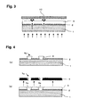
During exposure, as shown in Fig. 3, it is also
preferable to position an irregular reflection plate 10 on
the side opposite the glass plate 1 of the dry film 4 so
that the reflected light by the irregular reflection plate
(diffusion board) 10 shines on the dry film 4. Namely,
through this configuration, light initially passes dry film
4, is reflected by the irregular reflection plate 10, and
again shines toward the glass plate 1. Therefore, adding a
distance from the glass plate 1 widens the exposed area.
Furthermore, by appropriately selecting the etching
method for the dry film 4, etching of this type of tapered
dry film 4 is possible.
Then, when performed in this manner, the development
of S17, as shown in Fig. 4(a), enables the dry film 4 having
a wider area toward the top to remain. Therefore, as shown
in Fig. 4(b), the metal plating layer 6 formed by
electroplating has tapered sides, which are widest in area
on the Cr film 2 and smaller in area toward the top. Thus,
the metal mask 7 formed from the separated metal plating
layer 6 is shown in Fig. 4(b), and the smallest part of the
opening has the same shape as that of Cr film 2 from where
the opening increases in size in the direction of thickness
(toward the top in the figure).
The use of this metal mask defines the smallest part
of the opening, which has the same shape as that of the Cr
film 2. Therefore, a metal mask having extremely high
precision can be obtained.
Furthermore, when this metal mask is used as a vapor
deposition mask, an appropriate vapor deposition can be
performed. Namely, as EL panels increase in size, the plate
for vapor deposition also increases in size. If the opening
in the metal mask is straight while performing vapor
deposition on such a large plate, a difference in the vapor
deposited amount develops between the periphery and the
center. However, by tapering the opening of the metal mask,
it becomes possible for vapor deposition of material from a
diagonal direction at the periphery for a uniform vapor
deposited amount. Vapor deposition is performed with the
metal mask with the small side of the opening on the plate
side. In this way, the area on which vapor deposition is
performed can be maintained with accuracy.
S24 may be performed before the process of separating
the metal mask in S23. Namely, as shown in Fig. 5, after
electroplating is performed in S22, the dry film 4 is
removed (S24). Then, after the dry film 4 has been removed,
the metal mask 7 is separated (S23). Then, the glass plate 1
is returned to the surface treatment of S11. In this case,
chemicals that do not affect the metal mask 7 are used in
S24.
A method for manufacturing a metal mask for vapor
deposition for EL devices in the second embodiment of the
present invention will be described with reference to Fig.
6.
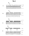
First, as shown in Fig. 6(a), in a manner identical to
the manufacturing method of the above-mentioned first
embodiment, for example, the photosensitive material (first
resist film) 3 with a thickness of 0.7 µm is formed on the
Cr film 2 with a thickness of 0.1 µm.
Next, by means of an electron beam exposure method,
laser beam exposure method, or the like, mask pattern 3a is
formed directly on photosensitive material 3. Then, with the
photosensitive material 3 used as a mask, Cr 2 film is
etched. As shown in Fig. 6(b), mask pattern 2a corresponding
to and preferably in the same shape as that of the mask
pattern 3a is formed on the Cr film 2. Thereafter,
photosensitive material 3 is separated (removed).
Then, as shown in Fig. 6(c), after pretreatment of Cr
film 2, a metal plating layer 11 is formed on the Cr film 2
by means of electroplating. The metal plating layer 11 is
formed from Ni, Ni-Co alloy, Ni-W alloy, or the like, and a
mask pattern 11a is formed in the same shape as that of the
mask pattern 2a.
Thereafter, as shown in Fig. 6(d), the metal plating
layer 11 is separated from Cr film 2 to form a metal mask 12
having a mask pattern 12a in the same shape as that of mask
pattern 2a.
Also, by repeating the steps shown in Figs. 6(c)-6(d),
multiple high precision metal masks 12 can be manufactured
in a simple process with each having the same precision.
By means of the method for manufacturing a metal mask
in this embodiment, the metal plating layer 11 is formed by
electroplating on the Cr film 2, after which the metal
plating layer 11 is separated from the Cr film 2 so as to
enable the dimensions of the mask pattern to be easily
controlled in the manufacturing process of the metal mask.
Furthermore, since the process is simplified, the
manufacturing cost can be reduced.
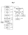
In the second embodiment, the procedure for
manufacturing the metal mask using the glass plate 1 on
which is formed the Cr film 2 is shown in Fig. 7.
As described above, the second embodiment does not
have processes for lamination, exposure, development, and so
forth for dry film 4. Therefore, compared to Fig. 2, the
processes S14-S20 are omitted and the process for S24 does
not exist. The remaining processes are performed in general
with conditions identical to those of the first embodiment.
The electroplating of S22 is performed without dry
film 4. Therefore, although the metal plating layer 11 is
formed on Cr film 2, it also extends on the side of Cr film
2 as shown in Fig. 8. Therefore, the shape of the metal mask
obtained in S23 is not exactly the same as that of the Cr
film 2. Therefore, when forming the Cr film 2 in the second
embodiment, it is preferable to set the dimensions while
taking into consideration that the opening will become
smaller from the electroplating.
In the above-mentioned first embodiment, the mask
pattern 4a to be the guide for the metal plating layer 6 was
formed using the dry film 4. Instead of this, a wet resist
can also be used. This process will be described with
reference to Figs. 9(a)-9(d).
First, as shown in Fig. 9(a), by means of vapor
deposition or sputtering, the Cr film 2 with a thickness of
0.1 µm, for example, is formed on the surface of the glass
plate 1. Then, by means of a spin coating method or the
like, the photosensitive material 3 with a thickness of 0.7
µm, for example, is formed on the Cr film 2.
Then, by means of an electron beam exposure method,
laser beam exposure method, or the like, mask pattern 3a is
directly formed on the photosensitive material 3. Then, the
Cr film 2 is etched with the photosensitive material 3 as a
mask, and as shown in Fig. 9(b), the mask pattern 2a having
the same shape as that of the mask pattern 3a is formed on
the Cr film 2.
Thereafter, as shown in Fig. 9(b), a second
photosensitive material 8 is formed on top of the
photosensitive material 3. The second photosensitive
material 8 is a liquid and also reaches inside the opening
of mask patterns 2a, 3a. Then, in this state, exposure is
performed from the back side of the glass plate 1. In this
way, the second photosensitive material 8 is exposed so as
to correspond to the mask pattern 2a on the Cr film 2.
Then, after exposure is completed, dry etching is
performed from the top. At this time, the second
photosensitive material 8 is etched at the unexposed
portion. Furthermore, the photosensitive material 3 is
etched. Therefore, by means of dry etching, as shown in Fig.
9(c), the portion exposed on the second photosensitive
material forms mask pattern 8a.
Next, electroplating is performed to form on the Cr
film 2 the metal plating layer 6, which is separated to
yield the metal mask 7.
According to this embodiment, the metal mask can be
obtained by using a wet photosensitive material without
using dry film.
The metal mask obtained in the above-mentioned manner
is preferably used as a vapor deposition mask for EL panels.
Namely, the EL panel has an EL element at every picture
element on the glass plate. The EL element has an electron
transport layer, an emissive layer, and a hole transport
layer between a cathode and an anode. Furthermore, the
active-type EL panel has a thin-film transistor (TFT)
corresponding to each EL element to control light emission
at each EL element. In the formation of an EL panel having
these EL elements, the necessary material layers are
laminated in sequence in a predetermined pattern. Then,
since a higher definition display is possible with smaller
picture elements, the metal mask of the present invention is
preferably used as a mask for the material lamination.
In particular, by using a magnetic material for the
metal mask, such as nickel, the metal mask can be secured
using magnetic force. Thus, the metal mask can be easily
secured on the surface to be laminated with materials.
Therefore, the metal mask of the present invention is
preferably a vapor deposition mask for EL panels.
The various embodiments of the method for
manufacturing a metal mask in the present invention have
been explained with reference to figures. However, actual
configurations are not limited to the various above-mentioned
embodiments so that variations and modifications
thereto are possible within the spirit and scope of the
present invention.
For example, in the method for manufacturing a metal
mask in the first and second embodiments, the glass plate 1
was used. However, the glass plate 1 is only for forming a
film of Cr or other electroconductive material, and in
addition to glass plate 1, it is also possible to use a
heat-resistant resin, heat-resistant resin film, or the
like. Furthermore, in the second embodiment, exposure is not
performed from the back side of glass plate 1. Therefore, it
is also possible to use a non-transparent plate instead of
the glass plate 1. For example, a ceramic plate or the like
may be used.
Also, instead of forming the mask pattern 3a directly
on the photosensitive material 3 by means of an electron
beam exposure method, laser beam exposure method, or the
like, a master mask can be used to expose the photosensitive
material to form mask pattern 3a on the photosensitive
material 3.
Also, in the aforementioned embodiments, Cr film 2 and
photosensitive material 3 are formed in sequence on the
surface of glass plate 1. However, a substrate with Cr film
2 can be first formed on the surface of glass plate 1, and
the photosensitive material 3 can be formed on Cr film 2 of
this substrate. Also, instead of Cr film 2, the film can be
a Cr-based alloy having a principle component of chromium or
an ITO film.
Also, dry film 4 is used. However, the dry film 4 may
be made of any photosensitive material, such as liquid
resist, or other liquid photosensitive resin.
Also, in addition to Ni, Ni-Co alloy, and Ni-W alloy,
any type of metal that can be formed by electroplating can
be used as the metal for forming metal plating layers 6, 11,
such as Ta (tantalum), Mo (molybdenum), W (tungsten), or the
like.
Also, electroplating is used in the aforementioned
embodiments. However, electroless plating can be used.
As described above, according to the present
invention, an electroconductive film having a mask pattern
is formed on one principle surface of a transparent plate or
a transparent film. Then, a photosensitive film is formed on
the electroconductive film. Then, with the electroconductive
film used as a mask, the photosensitive film is exposed from
the side of the transparent plate or transparent film to
form a mask pattern in the same shape as that of the mask
pattern on the photosensitive film. In this way, a
photosensitive film can be formed on an area on the
transparent plate or transparent film where there is no
electroconductive film. Therefore, it is easy to select a
material having a low coefficient of thermal expansion, such
as glass, for the transparent plate or transparent film so
as to eliminate changes over time in the dimensions of the
mask pattern. In this way, it is easy to control the
dimensions of the mask pattern in the process of
manufacturing the metal mask.
Also, with the photosensitive film used as a mask, a
metal plating layer is formed on the electroconductive film.
By separating the metal plating layer, it is easy to obtain
the metal mask having a pattern in the same shape as that of
the mask pattern formed on the photosensitive film.
Also, by repeating the step of forming the metal
plating layer on the electroconductive film and the step of
separating the metal plating layer, it is possible to form
multiple high-precision metal masks at the same precision.
Also, according to the present invention, an
electroconductive film having a mask pattern is formed on
one principle surface of a dielectric plate. Then, a metal
plating layer having a mask pattern in the same shape as
that of the mask pattern can be formed on the
electroconductive film. This metal plating layer is then
separated to form a metal mask. In this way, a material
having a low coefficient of thermal expansion, such as glass
or ceramic, can be used for the dielectric plate. It becomes
easy to control the dimensions of the mask pattern in the
process of manufacturing the metal mask. Also, according to
this method, the process is simplified so that the
manufacturing cost can be reduced.
Also, because the side of the opening in the metal
mask has a tapered shape, the precision of the mask pattern
can be improved. In particular, because the metal mask is
shaped so that the opening is smallest on the side close to
the electroconductive film, the mask pattern becomes
precisely the same as the electroconductive film.
Also, by shaping the photosensitive film into a
tapered shape, it becomes easy to obtain a metal mask having
a tapered opening.
As explained in the above, according to the present
invention, dimensional control in the manufacturing process
is easy so that multiple high-precision masks can be
manufactured at the same precision and the manufacturing
cost can be reduced.
Claims (14)
- A method for manufacturing a metal mask, comprising the steps of:(a) forming an electroconductive film having a mask pattern on one principle surface of a transparent plate or a transparent film;(b) forming a photosensitive film on the electroconductive film;(c) exposing said photosensitive film from side of said transparent plate or transparent film with said electroconductive film as a mask to form a mask pattern on the photosensitive film having the same shape as that of said mask pattern of the electroconductive film;(d) forming a metal plating layer on said electroconductive film; and(e) separating the metal plating layer to form the metal mask.
- A method for manufacturing a metal mask, comprising the steps of:(a) providing a substrate with an electroconductive film formed on one principle surface of a transparent plate or a transparent film;(b) forming a first resist film on the electroconductive film of the substrate;(c) forming a first mask pattern on the first resist film;(d) etching said electroconductive film with the resist film as a mask;(e) removing the first resist film;(f) forming a second resist film on the electroconductive film;(g) exposing the second resist film from side of said transparent plate or transparent film with said electroconductive film as a mask to form a second mask pattern on said second resist film;(h) forming a metal plating layer by electroplating on said electroconductive film; and(i) separating the metal plating layer to form the metal mask.
- The method for manufacturing a metal mask according to claim 2 characterized in that said second resist film is a dry film.
- The method for manufacturing a metal mask as in one of claims 1-3, in which the mask pattern formed on said second resist film includes an opening that narrows as the space on said electroconductive film is further from the electroconductive film.
- A method for manufacturing a metal mask, comprising the steps of:(a) providing a substrate with an electroconductive film formed on one principle surface of a transparent plate or a transparent film;(b) forming a first resist film on the electroconductive film of the substrate;(c) forming a first mask pattern on the first resist film;(d) etching said electroconductive film with the resist film as a mask;(e) removing the first resist film;(f) forming a metal plating layer by electroplating on said electroconductive film; and(g) separating the metal plating layer to form a metal mask having a mask pattern in the same shape as that of said first mask pattern.
- A method for manufacturing a metal mask, comprising the steps of:(a) providing a substrate with an electroconductive film formed on one principle surface of a dielectric plate;(b) forming a first resist film on the electroconductive film of the substrate;(c) forming a first mask pattern on the first resist film;(d) etching said electroconductive film with the resist film as a mask;(e) removing the first resist film;(f) forming a metal plating layer by electroplating on said electroconductive film; and(g) separating the metal plating layer to form a metal mask having a mask pattern in the same shape as that of said first mask pattern.
- The method for manufacturing a metal mask as in one of claims 2-6, in which the formation of the mask pattern on said first resist film is performed using an electron beam exposure method or a laser beam exposure method.
- The method for manufacturing a metal mask as in one of claims 2-6, in which the formation of the mask pattern on said first resist film is performed by the exposure method using a master mask.
- A method for manufacturing a metal mask, comprising the steps of:(a) forming an electroconductive film having a mask pattern on one principle surface of a transparent plate or a transparent film;(b) forming a metal plating layer on the electroconductive film; and(c) separating the metal plating layer to form a metal mask having a mask pattern with the same shape as that of said mask pattern.
- A method for manufacturing a metal mask, comprising the steps of:(a) forming an electroconductive film having a mask pattern on one principle surface of a dielectric plate;(b) forming a metal plating layer on the electroconductive film; and(c) separating the metal plating layer to form a metal mask having a mask pattern with the same shape as that of said mask pattern.
- The method for manufacturing a metal mask as in one of claims 1-10, in which said electroconductive film is a metal film that has a principle component of chromium.
- The method for manufacturing a metal mask as in one of claims 1-10, in which said electroconductive film is an ITO film.
- A metal mask manufactured by a manufacturing method as in one of claims 1-12.
- A metal mask obtained by separating a metal plating layer formed on a electroconductive film having a predetermined mask pattern formed on a dielectric plate wherein the metal mask has an opening with a tapered shape widening from the separated surface toward the opposite side and the widest opening is at side of the separated surface.
Applications Claiming Priority (3)
| Application Number | Priority Date | Filing Date | Title |
|---|---|---|---|
| JP2000292914A JP2002055461A (en) | 2000-05-29 | 2000-09-26 | Method for producing metallic mask |
| JP2000292914 | 2000-09-26 | ||
| PCT/JP2001/008309 WO2002027073A1 (en) | 2000-09-26 | 2001-09-25 | Method for producing metal mask and metal mask |
Publications (2)
| Publication Number | Publication Date |
|---|---|
| EP1327705A1 true EP1327705A1 (en) | 2003-07-16 |
| EP1327705A4 EP1327705A4 (en) | 2007-02-21 |
Family
ID=18775781
Family Applications (1)
| Application Number | Title | Priority Date | Filing Date |
|---|---|---|---|
| EP01967831A Withdrawn EP1327705A4 (en) | 2000-09-26 | 2001-09-25 | Method for producing metal mask and metal mask |
Country Status (6)
| Country | Link |
|---|---|
| US (2) | US7025865B2 (en) |
| EP (1) | EP1327705A4 (en) |
| KR (1) | KR100803455B1 (en) |
| CN (1) | CN1392905A (en) |
| TW (1) | TW497004B (en) |
| WO (1) | WO2002027073A1 (en) |
Families Citing this family (26)
| Publication number | Priority date | Publication date | Assignee | Title |
|---|---|---|---|---|
| US7332689B2 (en) * | 2002-02-26 | 2008-02-19 | Boston Scientific Scimed, Inc. | Tacking method and apparatus |
| KR100561705B1 (en) * | 2004-06-18 | 2006-03-15 | 전자부품연구원 | Metal mask fabrication method using nickel electroplating method and metal mask using the same |
| KR100626041B1 (en) | 2004-11-25 | 2006-09-20 | 삼성에스디아이 주식회사 | Thin film deposition mask of flat panel display device and manufacturing method thereof |
| KR100773588B1 (en) * | 2006-06-29 | 2007-11-05 | 한국과학기술원 | Polymer pattern forming method and metal thin film pattern, metal pattern, micro shutter, micro lens array stamper, plastic mold forming method |
| KR100786843B1 (en) * | 2006-10-18 | 2007-12-20 | 삼성에스디아이 주식회사 | Method of manufacturing a deposition mask of an organic light emitting display device |
| WO2009045028A2 (en) | 2007-10-01 | 2009-04-09 | Lg Chem, Ltd. | Method for manufacturing glass cliche using laser etching and apparatus for laser irradiation therefor |
| KR100962778B1 (en) * | 2007-12-13 | 2010-06-09 | 현대자동차주식회사 | Mask Making Method for Wood Pattern Formation |
| WO2013030871A1 (en) * | 2011-08-30 | 2013-03-07 | 西工業株式会社 | Holed foil electrolytic precipitation device |
| CN103203952B (en) * | 2012-01-16 | 2016-12-14 | 昆山允升吉光电科技有限公司 | A kind of processing technology of stepped formwork |
| CN103203960B (en) * | 2012-01-16 | 2017-03-15 | 昆山允升吉光电科技有限公司 | A kind of manufacture method of stepped formwork |
| CN103203956B (en) * | 2012-01-16 | 2016-12-14 | 昆山允升吉光电科技有限公司 | A kind of processing technology of stepped formwork |
| CN103882375B (en) * | 2014-03-12 | 2016-03-09 | 京东方科技集团股份有限公司 | A kind of mask plate and preparation method thereof |
| CN104357885A (en) * | 2014-10-15 | 2015-02-18 | 中航飞机股份有限公司西安飞机分公司 | Protection method for local chromium electroplating of shaft type part |
| KR102609073B1 (en) * | 2016-11-30 | 2023-12-05 | 엘지디스플레이 주식회사 | Mask for deposition, manufacturing method of the same |
| CN107164788B (en) * | 2017-05-23 | 2019-08-02 | 上海天马有机发光显示技术有限公司 | Mask plate and manufacturing method thereof |
| CN107065432A (en) * | 2017-05-27 | 2017-08-18 | 中国电子科技集团公司第四十研究所 | A kind of method for preparing chromium plate mask plate |
| CN109216405A (en) * | 2017-06-30 | 2019-01-15 | 苏州苏大维格光电科技股份有限公司 | The manufacturing method of AMOLED metal mask plate |
| CN107365958B (en) * | 2017-07-13 | 2020-01-07 | 上海天马有机发光显示技术有限公司 | Preparation method of metal mask |
| CN110670014A (en) * | 2018-07-03 | 2020-01-10 | 上海和辉光电有限公司 | Mother plate core mold, mask plate and manufacturing method thereof |
| CN108796440A (en) * | 2018-07-26 | 2018-11-13 | 京东方科技集团股份有限公司 | A kind of preparation method of mask plate, mask plate, evaporated device |
| CN109898104A (en) * | 2019-02-20 | 2019-06-18 | 合肥永淇智材科技有限公司 | A kind of FMM electroforming motherboard production method of conical mouths |
| CN114574908B (en) * | 2019-05-13 | 2022-11-25 | 创造未来有限公司 | Method for manufacturing fine metal mask |
| KR102304697B1 (en) | 2020-05-27 | 2021-09-24 | (주)엠시스 | An Apparatus for Investigating a Metal Mask |
| TWI825368B (en) * | 2020-12-07 | 2023-12-11 | 達運精密工業股份有限公司 | Method of manufacturing metal mask |
| JP2022127384A (en) * | 2021-02-19 | 2022-08-31 | 株式会社ジャパンディスプレイ | Production method of vapor deposition mask |
| CN117031889B (en) * | 2023-08-29 | 2024-04-02 | 无锡市华辰芯光半导体科技有限公司 | A single-layer positive photoresist photolithography method |
Family Cites Families (11)
| Publication number | Priority date | Publication date | Assignee | Title |
|---|---|---|---|---|
| US3900359A (en) * | 1973-02-26 | 1975-08-19 | Dynamics Res Corp | Method and apparatus for television tube shadow mask |
| US4306925A (en) * | 1977-01-11 | 1981-12-22 | Pactel Corporation | Method of manufacturing high density printed circuit |
| DE2828625C2 (en) * | 1978-06-29 | 1980-06-19 | Siemens Ag, 1000 Berlin Und 8000 Muenchen | Process for the electroforming production of precision flat parts |
| JPS60141887A (en) * | 1983-12-28 | 1985-07-26 | Seiko Epson Corp | Manufacture of electroformed precision parts |
| JPH06938A (en) * | 1992-06-19 | 1994-01-11 | Shinwa:Kk | Metal mask and manufacturing method thereof |
| US5686207A (en) * | 1994-08-08 | 1997-11-11 | Seiko Instruments Inc. | Method of forming and repairing a mask for photolithography |
| US5560837A (en) * | 1994-11-08 | 1996-10-01 | Hewlett-Packard Company | Method of making ink-jet component |
| WO1997046390A1 (en) * | 1996-06-04 | 1997-12-11 | Citizen Watch Co., Ltd. | Ink jet head and method of manufacturing same |
| JPH11138827A (en) * | 1997-11-10 | 1999-05-25 | Citizen Watch Co Ltd | Manufacture for minute part |
| JPH11172487A (en) * | 1997-12-05 | 1999-06-29 | Citizen Watch Co Ltd | Production of fine electroformed parts |
| US6179978B1 (en) * | 1999-02-12 | 2001-01-30 | Eastman Kodak Company | Mandrel for forming a nozzle plate having a non-wetting surface of uniform thickness and an orifice wall of tapered contour, and method of making the mandrel |
-
2001
- 2001-09-25 US US10/129,877 patent/US7025865B2/en not_active Expired - Lifetime
- 2001-09-25 KR KR1020027006698A patent/KR100803455B1/en not_active Expired - Lifetime
- 2001-09-25 CN CN01802920A patent/CN1392905A/en active Pending
- 2001-09-25 EP EP01967831A patent/EP1327705A4/en not_active Withdrawn
- 2001-09-25 WO PCT/JP2001/008309 patent/WO2002027073A1/en not_active Ceased
- 2001-09-26 TW TW090123744A patent/TW497004B/en not_active IP Right Cessation
-
2005
- 2005-12-01 US US11/292,760 patent/US20060204904A1/en not_active Abandoned
Also Published As
| Publication number | Publication date |
|---|---|
| EP1327705A4 (en) | 2007-02-21 |
| US20060204904A1 (en) | 2006-09-14 |
| CN1392905A (en) | 2003-01-22 |
| WO2002027073A1 (en) | 2002-04-04 |
| KR100803455B1 (en) | 2008-02-14 |
| US7025865B2 (en) | 2006-04-11 |
| US20020164534A1 (en) | 2002-11-07 |
| TW497004B (en) | 2002-08-01 |
| KR20030009324A (en) | 2003-01-29 |
Similar Documents
| Publication | Publication Date | Title |
|---|---|---|
| US7025865B2 (en) | Method for producing metal mask and metal mask | |
| US8070970B2 (en) | UV-LIGA process for fabricating a multilayer metal structure having adjacent layers that are not entirely superposed, and the structure obtained | |
| JP2003107723A (en) | Manufacturing method for metal mask and metal mask | |
| CN108073035A (en) | A kind of restorative procedure of lithography mask version and lithography mask version defect | |
| CN117406319A (en) | Processing method of relief helical grating | |
| US4556608A (en) | Photomask blank and photomask | |
| EP0273392B1 (en) | Multi-layer structure and method of fabrication thereof | |
| JP2021096249A (en) | Method of manufacturing timepiece component and component produced using the same | |
| JP3605567B2 (en) | Method for forming transparent conductive film using chemically amplified resist | |
| US5755947A (en) | Adhesion enhancement for underplating problem | |
| EP0103844B1 (en) | X-ray mask | |
| US7354699B2 (en) | Method for producing alignment mark | |
| KR101250411B1 (en) | High Definition Printing Plate of Liquid Crystal Display and Method for Manufacture using the same | |
| CN121578592B (en) | Multi-stage fine alignment method for complex micro-nano structure | |
| US20010028986A1 (en) | Transfer layer repair process for attenuated masks | |
| JP2001350269A (en) | Method for producing mask for solder printing | |
| JP2002055461A (en) | Method for producing metallic mask | |
| KR20140050456A (en) | Photo film mask including dlc pattern and manufacturing method thereof | |
| CN118164427A (en) | Preparation method of template with micron-sized oxide insulating layer hole array | |
| JPH07113193A (en) | Production of metal mold for molding diffraction grating | |
| CN121578592A (en) | A multi-level fine overlay method for complex micro/nano structures | |
| JPH11149152A (en) | Grounding method and photomask blanks | |
| KR100501768B1 (en) | X-ray mask and manufacturing method there of | |
| CN116224711A (en) | Manufacturing method of photomask | |
| TW202538436A (en) | Method for manufacturing watch components in batches |
Legal Events
| Date | Code | Title | Description |
|---|---|---|---|
| PUAI | Public reference made under article 153(3) epc to a published international application that has entered the european phase |
Free format text: ORIGINAL CODE: 0009012 |
|
| 17P | Request for examination filed |
Effective date: 20020518 |
|
| AK | Designated contracting states |
Designated state(s): AT BE CH CY DE DK ES FI FR GB GR IE IT LI LU MC NL PT SE TR |
|
| A4 | Supplementary search report drawn up and despatched |
Effective date: 20070118 |
|
| STAA | Information on the status of an ep patent application or granted ep patent |
Free format text: STATUS: THE APPLICATION IS DEEMED TO BE WITHDRAWN |
|
| 18D | Application deemed to be withdrawn |
Effective date: 20070417 |