EP1324232A2 - Gerät, Verfahren und Programm zur Verifizierung eines Lsi-Entwurfs - Google Patents
Gerät, Verfahren und Programm zur Verifizierung eines Lsi-Entwurfs Download PDFInfo
- Publication number
- EP1324232A2 EP1324232A2 EP02028782A EP02028782A EP1324232A2 EP 1324232 A2 EP1324232 A2 EP 1324232A2 EP 02028782 A EP02028782 A EP 02028782A EP 02028782 A EP02028782 A EP 02028782A EP 1324232 A2 EP1324232 A2 EP 1324232A2
- Authority
- EP
- European Patent Office
- Prior art keywords
- description
- property
- module
- signal
- test bench
- Prior art date
- Legal status (The legal status is an assumption and is not a legal conclusion. Google has not performed a legal analysis and makes no representation as to the accuracy of the status listed.)
- Withdrawn
Links
Images

















Classifications
-
- G—PHYSICS
- G06—COMPUTING OR CALCULATING; COUNTING
- G06F—ELECTRIC DIGITAL DATA PROCESSING
- G06F30/00—Computer-aided design [CAD]
- G06F30/30—Circuit design
- G06F30/32—Circuit design at the digital level
- G06F30/33—Design verification, e.g. functional simulation or model checking
- G06F30/3323—Design verification, e.g. functional simulation or model checking using formal methods, e.g. equivalence checking or property checking
Definitions
- the present invention relates to an LSI design verification apparatus, an LSI design verification method, and an LSI design verification program for comparing properties and circuit descriptions which are parts of formal verification.
- RTL register transfer level
- gate-level netlist corresponds to representation of a circuit configuration through use of logic formulas of gate elements.
- mask patterns are formed from an upper side of the gate level description, thus manufacturing an actual semiconductor integrated circuit.
- the formal verification described here has two meanings, i.e., a property check and logic equivalence verification.
- the "property check” means verification as to whether or not a designed logical circuit satisfies design specifications (or properties).
- the "logic equivalence verification” means verification as to whether or not two circuits are logically equivalence to each other. However, in the logic equivalent verification, only equivalence between the two circuits can be verified, but it is not known whether or not logical functions intended by a designer have been realized. In order to verify this realization, for example, a simulation or a property check must be carried out.
- An apparatus for design verification using logical simulation of a circuit description, having a plurality of hierarchies from top to bottom in accordance with abstraction levels of circuit components includes: a circuit description reading unit configured to read the circuit description; an analysis unit configured to analyze signal connection topologies between the hierarchies of the circuit description from top to bottom; a data storing unit configured to store data of the signal connection topologies; a property reading unit configured to read properties of target modules implemented by the circuit components in the circuit description; an inter-module property extraction unit configured to extract a property part having a signal communicating between the target modules; a signal operation portion extraction unit configured to extract output operation properties, defining output operation of an output side module, and an expecting operation property, defining an expecting operation of an input side module among the properties of the target modules; and a comparing unit configured to compare the output operation properties with the expecting operation properties.
- An apparatus for design verification using logical simulation of a circuit description, a plurality of hierarchies from top to bottom in accordance with abstraction of circuit components includes: a circuit description reading unit configured to read the circuit description; an analysis unit configured to analyze a signal connection topologies between the hierarchies of the circuit description from top to bottom; a property generation unit configured to generate a property description constituted by a signal topology connected to a target module from the property description of a module providing an input to the target module, the target module being implemented by the circuit component; a first test bench generation unit configured to generate a test vector and a first test bench description; and a second test bench generation unit configured to generate a second test bench description for comparing a simulation output and a specification output from the property description of the target module.
- a computer implemented method for design verification using logical simulation of a circuit description having a plurality of hierarchies from top to bottom in accordance with abstraction of circuit components includes: reading the circuit description; analyzing signal connection topologies between the hierarchies of the circuit description from top to bottom; storing data of the signal connection topologies to a data storing device; reading properties of target modules implemented by the circuit components in the circuit description: extracting a property part having a signal communicating between the target modules; extracting an output operation property, defining output operation in an output side module, and an expecting operation property, defining an expecting operation of an input side module among the properties of the target module; and comparing the output operation properties with the expecting operation properties.
- a computer implemented method for design verification using logical simulation of a circuit description having a plurality of hierarchies from top to bottom in accordance with abstraction of circuit components includes: reading the circuit description; analyzing signal connection topologies between the hierarchies of the circuit description from top to bottom; generating a property description constituted by a signal topology connected to a target module from the property description of a module providing an input to the target module, the target module being implemented by the circuit components; generating a test vector and a first test bench description; and generating a second test bench description comparing a simulation output and a specification outputs from the property description of the target module.
- a computer program product for use with a design verification apparatus wherein the apparatus uses logical simulation of a circuit description having a plurality of hierarchies from top to bottom in accordance with abstraction of circuit components
- the computer program product includes: instructions configured to read the circuit description; instructions configured to analyze signal connection topologies between the hierarchies of the circuit description from top to bottom; instructions configured to store data of the signal connection topologies to a data storing device; instructions configured to read properties of target modules implemented by the circuit components in the circuit description; instructions configured to extract a property part having a signal communicating between the target modules; instructions configured to extract an output operation property, defining output operation in an output side module, and an expecting operation property, defining an expecting operation of an input side module among the properties of the target module; and instructions configured to compare the output operation properties with the expecting operation properties.
- a computer program product for use with a design verification apparatus wherein the apparatus uses logical simulation of a circuit description having a plurality of hierarchies from top to bottom in accordance with abstraction of circuit components
- the computer program product includes: instructions configured to read the circuit description; instructions configured to analyze signal topology connection topologies between the hierarchies of the circuit description from top to bottom; instructions configured to generate a property description constituted by a signal connected to a target module from the property description of a module providing an input to the target module, the target module being implemented by the circuit component; instructions configured to generate a test vector and a first test bench description; and instructions configured to generate a second test bench description comparing a simulation output and a specification output from the property description of the target module.
- An LSI design verification apparatus 1 of a first embodiment shown in FIG. 1 includes at least a central processing unit (CPU) 2, an input device 31 and an output device 32 connected through an input/output control device 33 to the CPU 2, a data storage device 4 connected to the CPU 2, and a main memory 35.
- the CPU 2 is provided with a database management unit for which the drawing is omitted. When an input/output with the data storage device 4 is necessary, a storage place of a necessary file is searched to read out/write the file through this database management unit.
- the CPU 2 includes at least a data storing unit 9, a circuit description reading unit 10, an analysis unit 11, a property reading unit 12, an inter-module property extraction unit 13, a signal operation portion extraction unit 14, a comparator 15, a mismatch detector 16, a report generator 17, a redundant portion deletion unit 18, a register insertion unit 19, and a display unit 20.
- the data storing unit 9 controls storing data on a signal connection relation between hierarchies in the data storage device 4.
- the circuit description reading unit 10 reads circuit description of an experimental circuit in the LSI design verification apparatus 1.
- the analysis unit 11 analyzes a connection relation and a signal input/output relationship between modules, such that a multiplier (MULT) 46, a controller (CON) 48, and an arithmetic and logic unit (ALU) in a TOP module 45 shown in FIG.2 and FIG.3, in a top hierarchy for the circuit description.
- the property reading unit 12 reads properties of each module to be verified from the data storage device 4 in the LSI design verification apparatus 1.
- the inter-module property extraction unit 13 extracts a section including a signal between the modules (hereinafter, referred to as "inter-module signal properties") from the read properties of each module to be verified.
- the signal operation portion extraction unit 14 extracts signal operation portions of properties that exist in a module of a signal output side to define an output operation (referred to as “output operation properties”, hereinafter), and also extracts properties that exist in an input side module to define an expected operation (referred to as “expected operation properties”, hereinafter) from the extracted inter-module signal properties.
- the comparator 15 compares properties of output and input sides of each signal by using the signal operation portions of the output operation properties and the expected operation properties.
- the mismatch detector 16 compares conditions of the properties to detect mismatched conditions if a result of the comparison specifies a common signal between the modules to be verified is specified. This common signal is described as a property condition.
- the report generator 17 generates an error report if mismatched conditions are detected by the mismatch detector 16.
- the redundant portion deletion unit 18 deletes a signal redundant portion if interface specifications have room, and a hierarchical design method is not used.
- the register insertion unit 19 inserts a register into a hierarchical boundary of a signal if interface specifications have room, and the hierarchical design method is used.
- the display unit 20 displays a transient waveform of the signal regarding a mismatched content based on the report transferred from the report generator 17.
- the input device 31 includes a keyboard, a mouse, a recognition device such as an optical character reader (OCR), a graphic input device such as an image scanner, and a special input device such as a voice recognition device.
- the output device 32 includes a display device such as a liquid crystal display (LCD) or a cathode ray tube (CRT) display, and a printer such as an ink jet printer or a laser printer.
- the input/output control device (input/output interface) 33 is an interface for connecting the input device 31, the output device 32, and a reading unit which reads data from an external storage medium, such as a compact disk ROM, a magnetic optical disk (MO) or a flexible disk (FD), to the CPU 2.
- the input/output control unit 33 works as an interface for the input device 31, the output device 32, and the reading unit of the external storage device.
- the main memory 35 includes a read only memory (ROM) and a random access memory (RAM).
- the ROM functions as a program memory for storing programs to be executed in the CPU 2.
- the RAM functions as a temporary data memory used as a working area for temporarily storing data used during program execution in the CPU 2.
- the data storage device 4 stores circuit description information for an module names (or an top hierarchies) in a module unit.
- the experimental circuit 45 used in the first embodiment of the present invention includes a top hierarchy (TOP) and a second hierarchy (lower hierarchy), which is constituted of a multiplier (MULT) 46, an arithmetic logic unit (ALU) 47, and a controller (CON) 48.
- TOP top hierarchy
- MULT multiplier
- ALU arithmetic logic unit
- CON controller
- FIG. 3 shows the data structure of the data storage device 4.
- the data storage device 4 stores a module name of a top hierarchy (first section), a module name included in the module of the top hierarchy (second section), a combination of each module (third section), connection information between modules (fourth section), property information regarding an extracted signal (fifth section), and property information converted for each combination of signals (sixth section) for each module.
- a result such as that shown in FIG.2 from the analysis of the top hierarchy as shown in FIG. 3, first, a module name of the top hierarchy "TOP" is stored in the first section of the data storage device 4. Then, the module name included in the "TOP 45" is stored in the second section.
- the multiplier (MULT) 46, the controller (CON) 48, and the arithmetic logic unit (ALU) 47 are stored in the second section.
- combination information of the modules stored in the second section is stored.
- the multiplier (MULT) 46 since a combination of the controller (CON) 48 and the arithmetic logic unit (ALU) 46 is extracted, the CON 48 and the ALU 47 are stored in the third section corresponding to the MULT 46 of the second section.
- the CON 48 since a combination of the MULT 46 and the ALU 47 is extracted, the MULT 46 and the ALU 47 are stored in the third section corresponding to the CON 48 of the second section.
- the ALU 47 since a combination of the MULT 46 and the CON 48 is extracted, the MULT 46 and the CON 48 are stored in the third section corresponding to the ALU 47 of the second section.
- connection information between the modules extracted in the second section is stored.
- the multiplier (MULT) 46 of the second section combinations of the MULT 46 with the controller (CON), and the MULT 46 with the arithmetic logic unit (ALU) 47 are extracted from the third section, and connection relations of these two combinations are stored in the fourth section.
- a connection relation between the MULT 46 and the CON 48 a connection relation of the MULT 46 and the CON 48, i.e., "MULT: STB (STB), Done (Done), R_M(R_M)/CON: STB(STB), Done (Done), R_M(R_M)"
- STB connection relation between the MULT 46 and the ALU 47
- property information regarding the extracted signal is stored. That is, property information regarding the signal (STB, Done, R_M) extracted in the fourth section as the connection relation between the module multiplier (MULT) 46 and the controller (CON) 48 is extracted from properties of each of the MULT 46 and the CON 48 to be stored in the fifth section.
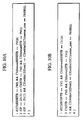
- properties including the signal "STB, Done, R_M" extracted in the fourth section in the MULT 46 side, property information shown in FIG. 4A is extracted, and in the CON 48 side, property information shown in FIG. 4B is extracted, to be stored in the fifth section.
- property information converted for each combination of signals is stored for each module. That is, properties of a related signal operation extracted from the properties of the fifth section, excluding the properties of an unrelated signal between the two modules, are stored in the sixth section.
- FIG. 4A shows an example of properties for single verification of the multiplier (MULT) 46 as one of the modules.
- STB starting signal
- B a value of the signal B
- verification is made as to the completion of an operation in 11 to 15 cycles.
- Reference code C in FIG. 4A denotes a cycle, and "C1" means a case after 1 cycle.
- FIG. 4B shows an example of properties for single verification of the controller (CON) 48.
- two operations are verified.
- One of the operations to be verified is that when the external input signal (OP) is multiplication (2'11) after disenabling the reset condition, the starting signal (STB) asserts 1 after 3 cycles.
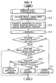
- the LSI design verification method, shown in FIG.5, according to the first embodiment of the present invention is described as follows.
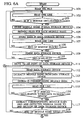
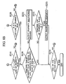
- step S11 shown in FIG.5 the process for generating a signal list 40 indicating a connection relation of signals between modules from a top hierarchy to a lower hierarchy (second hierarchy) in processes from step S101 to step S136 of FIG.6A and FIG.6B is described here as METHOD 1.
- METHOD 1 the procedures generating the multiplier (MULT) 6, the controller (CON) 48, and the arithmetic logic unit (ALU) 47 shown in FIG.2 and storing them in the data storage device 4 are described.
- comparison is made to a relation between the MULT 46 and the CON 48 here.
- the method for detecting and extracting property is to detect and to extract a property part including an interface signal between the controller (CON) 48 and the multiplier (MULT) 46, which are lower hierarchies (the second hierarchies) modules, from the signal list 40 stored in the data storage device 4.
- CON controller
- MULT multiplier
- step S13 a process for extracting signal operation portions of properties, defining an output operation in the output side modules of each signals and an expected operation in the input side modules of each signal from signal properties between the modules extracted in step S12 will be described with reference to FIG.9.
- step S324 shown in FIG.9 A specific example for processes in step S324 shown in FIG.9 will be described as follows.
- a termination signal Done
- STB starting signal
- the output side is the CON 48
- the input side the MULT 46.
- a left side of the properties of the MULT 46 becomes a condition for generating the termination signal (Done).
- the left side includes the starting signal (STB) and a signal B.
- step S15 shown in FIG.5 a process for comparing properties of the MULT 46 and the CON 48 will be described with reference to FIG.11.
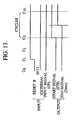
- step S16 a description will be made of an embodiment when there is mismatch between properties, with reference to FIG.5 and FIG.13.
- step S15 in processes from step S401 to step S414 of FIG. 11, property comparison is carried out between the multiplier (MULT) 46 and the controller (CON) 48.
- MULT multiplier
- CON controller
- step S20 a method and a process for inserting a register to redundant portions when there are two cycles of a redundant portion within CON 48 with reference to FIG.12.
- the process from step S411 to step S414 is similar to that of method 2, the differences will be briefly described in method 3.
- the flip-flop circuit can be inserted immediately after the termination signal (Done) in the CON 48.
- the first embodiment of the present invention by making a list of connection relation between hierarchies, properties regarding inter-hierarchy interface are extracted from properties (group) independently prepared in the lower hierarchy (second hierarchy), thus enabling a hierarchical property checking method.
- properties regarding inter-hierarchy interface are extracted from properties (group) independently prepared in the lower hierarchy (second hierarchy), thus enabling a hierarchical property checking method.
- an operation of transferring inter-hierarchy signals can be clearly defined.
- a plurality of properties regarding target signals are integrated, and optimized to clearly define the operation of transferring inter-hierarchy signals.
- inter-hierarchy properties are compared to detect mismatch in interface portions.
- the interface of the top hierarchy can be verified to carry out verification for a large circuit.
- the quality of the property checking method can be improved.
- the efficiency of the property checking method can be increased.
- the specifying mismatched places is facilitated by displaying mismatched interface between hierarchies in a waveform.
- the interface of the top hierarchy can be verified to carry out verification for a large circuit.
- register insertion into the hierarchy boundary to facilitate delay calculation in processing after logic synthesis can be surely executed without incursion of any defects.
- redundant portions in specifications can be deleted with certain and without the incursion of any defects, thus enabling the productivity of high-quality circuit description.
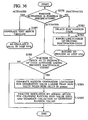
- FIG. 14 shows a conceptual diagram showing an LSI design verification method according to a second embodiment of the present invention.
- An integrated simulation environment 80 shown in FIG. 14 includes top test bench description (language for verification) 68 in logical simulation, driving test bench description (language for verification) 61 in the logical simulation, expected value checking test bench description (language for verification) 67 in the logical simulation, and top testing model description (HDL) 64 of a verification target module.
- top test bench description language for verification
- driving test bench description language for verification
- expected value checking test bench description language for verification
- HDL top testing model description
- a verification target is a module T
- the verification target module T is analyzed from model description M(TOP) of a top module to obtain an input connection relation (C(I)) of model description of a module I (M(I)) 60 that gives an input to the verification target module T, and an input connection relation (C(T)) of the verification target module T.
- the driving test bench description 61 is generated based on property description (property language) 62 of the module I that gives an input to the verification target module T.
- the checking test bench description 67 is generated based on property description (property language) 66 of the verification target module T.
- the top test bench description 68 is includes the driving test bench description 61, and the checking test bench description 67.
- the top testing model description 64 is generated from model description 63 of the verification target module T. Further, the model description 63 reports inactivation codes by a report 65.
- An LSI design verification apparatus 1 according to the second embodiment of the present invention shown in FIG. 15 comprises, as described above with reference to the first embodiment of the invention, at least a central processing unit (CPU) 2, an input device 31 and an output device 32 connected through an input/output control device 33 to the CPU 2, a data storage device 4 connected to the CPU 2 and a main memory 35.
- the CPU 2 is provided with a database management unit for which the drawing is omitted.
- the CPU 2 includes at least a circuit description reading unit 10, an analysis unit 11, a property generation unit 21, a driving test bench generation unit 22, a checking test bench generation unit 23, a top test bench generation unit 24, a top model generation unit 25, a logical simulation unit 26, a code coverage measurement unit 27, and an automatic determination unit 28.
- the circuit description reading unit 10 reads a circuit description of an experimental circuit in the LSI design verification apparatus 1.
- the analysis unit 11 analyzes a connection relation and a signal input/output relationship between modules from a top hierarchy, for the read circuit description.
- the property generation unit 21 generates property description includes a signal connected to a verification target module from a property description that gives an input to the verification target module.
- the driving test bench generation unit 22 generates a test vector from the property description, and driving test bench description to be inputted.
- the checking test bench generation unit 23 generates a checking test bench description for comparing an output in simulation with an output in specifications from the property description of the verification target module.
- the top test bench generation unit 24 generates top test bench description for a top hierarchy from the driving test bench description and the checking test bench description to execute these in parallel.
- the top model generation unit 25 generates top model description for simulation that becomes an interface with the model description of the verification target module.
- the logical simulation unit 26 performs logical simulation in the simulation environment including the driving test bench description, the checking test bench description, the top test bench description, and the top model description.
- the code coverage measurement unit 27 executes code coverage measurement.
- the automatic determination unit 28 automatically determines whether or not an inactivation code reported by the code coverage measurement can be activated in specifications based on the property description of the module that gives an input to the verification target module.
- FIG. 17 is a circuit diagram of the experimental circuit used in the second embodiment of the present invention.
- FIG. 18 shows a module constitution in the experimental circuit ALU used in the second embodiment of the present invention.
- the experimental circuit used in the second embodiment of the present invention comprises a top hierarchy (TOP) 75, and a controller (CON) 76 and an arithmetic logic unit A(ALU) 77 which includes a second hierarchy (lower hierarchy).
- TOP top hierarchy
- CON controller
- A(ALU) 77 which includes a second hierarchy (lower hierarchy).
- step S31 shown in FIG. 19 Details of the step S31 shown in FIG. 19 will be described with reference to FIG.20.
- FIG.21 A module structure of an executed circuit according to the second embodiment of the present invention is shown in FIG.21.
- a module name is written on a left side of a bracket, and an instance name in HDL description in the bracket, for example "module name (instance name in the HDL description)".
- a top circuit TOP 75 includes a controller (CON) 76, and an arithmetic logic unit (ALU) 77.
- the ALU 77 has a register selection controller (SELECTOR), a register for holding data A (AREG), a register for holding data B (BREG), a register for holding operator OP (OREG), an arithmetic logic circuit (alu8), and a register R for holding an operation result OUT (RREG).
- SELECTOR register selection controller
- A register for holding data A
- B register for holding data B
- ORG register for holding operator OP
- alu8 arithmetic logic circuit
- RREG a register R for holding an operation result OUT
- An input connection relation C(CON) of the controller (CON) 76 is shown in FIG.22A, and an input connection relation C(ALU) of the ALU 77 is shown in FIG.22B.
- an external input signal PI.CLK indicates a signal CON.CLK of the CON 76
- an external input signal PI.IN indicates an input signal CON.CIN of the CON 76.
- an external input signal PI.CLK indicates a signal ALU.CLK of the ALU 77
- an output signal CON.COUT of the CON 76 indicates an input signal ALU.AIN of the ALU 77
- a signal CON.CSEL of the CON 76 indicates a signal ALU.ASEL of the ALU 77
- a reset signal CON.CRESET of the CON 76 indicates a resent signal ALU.ARESET of the ALU 77.
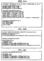
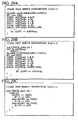
- step S32 shown in FIG.19 details of the property description used in step S32 shown in FIG.19 will be described with reference to FIG.24A, FIG.24B, and FIG.24C.
- the property description of a module T, P(T) 66. is described as a property description for a single verification P(ALU) of the module ALU 77, shown in FIG.24A, in the following description.
- the property description of a module I, P(I) 62 is described as a property description for a single verification P(CON) of the module CON 76, shown in FIG.24B, in the following description.
- the property description for the single verification P(ALU) of the module ALU 77 includes property descriptions P(ALU-1), P(ALU-2) and P(ALU-3) for verifying the operations (i), (ii) and (iii) of the ALU 77 in an interface specifications of the executed circuit described above.
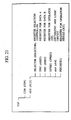
- step S32 a method for extracting relational property will be explained with reference to FIG. 23.
- a driving test bench T(drive) 61 is generated from the property description P(I->T) 74, which is P(COM->ALU) in FIG.23C, with reference to FIG. 25 from step S514 to S526.
- the test bench description includes a task section and a class declaration section.
- the driving test bench description T(drive) 61 includes a driving task section test bench description T(drive_TASK) 61a and a driving class declaration section test bench description T(drive_DECLARE) 61b.
- the drive_TASK 61a is obtained by executing the processes from step S514 to S526 to the property description P(I->T) 74.
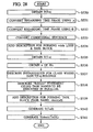
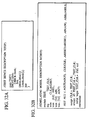
- step S34 shown in FIG.19 generation of the checking test bench description T(check) 67 will be explained with reference to FIG.28.
- the checking test bench description T(check) 67 includes a checking task section test bench description T(check_TASK) 67a and a checking class declaration section test bench description T(check_DECLARE) 67b.
- the checking task section test bench description T(check_TASK) 67a generated before the checking test bench description T(check) 67 is generated, includes a property checking test bench description T(T-n), which is obtained by converting the property description P(T-n) of the module T, and a concurrent processing test bench description T(T-all), for executing all the forgoing tasks in parallel.
- the property checking test bench description T(T-n) is generated.
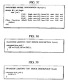
- step S35 generation of the model description M(TEST) 64 and the test bench description T(TOP) 68 will be explained with reference to FIG.31.
- step S542 the driving test bench description T(drive) 61, the checking test bench description T(check) 67 are concurrently executed, and the top test bench description T(TOP) 68, which is positioned above the T(drive) 61 and T(check) 67, is generated.
- step S36 corresponding to step S36 through step S39 in FIG.19, a process for executing a logical simulation will be described with reference to FIG.33.
- step S4 in FIG.19 a process for determining whether or not there is any possibility for activating an interface specification from the property description P(I->T) acquired in step S512 will be described with reference to FIG.35.
- step S40 corresponding to step S40 through step S45 in FIG.19, a process for determining whether or not there is any possibility for activating an interface specification from the property description P(U->T) will be described with reference to FIG.36.
- the second embodiment of the present invention by automatically generating reliable driving test bench description from property description of a module, which gives an input to a verification target module and where there are no errors or omissions of specifications, time regarding test bench description and simulation time by generating a test vector, valid within specifications, are able to be shorten.
- the second embodiment of the present invention by automatically determining whether or not an inactivation code cannot be activated based on insufficient test patterns or because of specifications, it is possible to prevent erroneous deletion of the inactivation in the former case, and enable the omission of useless simulation time in the latter case.
- the second embodiment of the present invention by deleting an inactivation code determined impossible to be activated in specifications, it is possible to reduce an area.
- by automatically generating random value generation limitation test bench description for activating an inactivation code, determined possible to be activated in specifications, and by reading this description to execute simulation it is possible to increase verification accuracy by activating the inactivation code.
- the function of the LSI verification system of the first and second embodiment of the present invention may be programmed and saved in a computer-readable recording medium.
- the programs saved in the recording medium is transferred to a memory in a computer system and then operated by its operating unit, thus putting the method in practice.
- the recording medium may be selected from semiconductor memories, magnetic disks, optical disks, optomagnetic disks, magnetic tapes, and any of the computer-readable recording mediums.
Landscapes
- Engineering & Computer Science (AREA)
- Computer Hardware Design (AREA)
- Physics & Mathematics (AREA)
- Theoretical Computer Science (AREA)
- Evolutionary Computation (AREA)
- Geometry (AREA)
- General Engineering & Computer Science (AREA)
- General Physics & Mathematics (AREA)
- Design And Manufacture Of Integrated Circuits (AREA)
- Tests Of Electronic Circuits (AREA)
Applications Claiming Priority (2)
| Application Number | Priority Date | Filing Date | Title |
|---|---|---|---|
| JP2001398319A JP3848157B2 (ja) | 2001-12-27 | 2001-12-27 | Lsi設計検証装置、lsi設計検証方法、及びlsi設計検証プログラム |
| JP2001398319 | 2001-12-27 |
Publications (2)
| Publication Number | Publication Date |
|---|---|
| EP1324232A2 true EP1324232A2 (de) | 2003-07-02 |
| EP1324232A3 EP1324232A3 (de) | 2009-09-09 |
Family
ID=19189333
Family Applications (1)
| Application Number | Title | Priority Date | Filing Date |
|---|---|---|---|
| EP02028782A Withdrawn EP1324232A3 (de) | 2001-12-27 | 2002-12-23 | Gerät, Verfahren und Programm zur Verifizierung eines Lsi-Entwurfs |
Country Status (3)
| Country | Link |
|---|---|
| US (1) | US20030125920A1 (de) |
| EP (1) | EP1324232A3 (de) |
| JP (1) | JP3848157B2 (de) |
Cited By (2)
| Publication number | Priority date | Publication date | Assignee | Title |
|---|---|---|---|---|
| CN100349416C (zh) * | 2004-12-01 | 2007-11-14 | 华为技术有限公司 | 一种激励数据的流量控制方法及装置、激励报文产生器 |
| CN104516992A (zh) * | 2013-09-27 | 2015-04-15 | 华为技术有限公司 | 一种验证方法及装置 |
Families Citing this family (29)
| Publication number | Priority date | Publication date | Assignee | Title |
|---|---|---|---|---|
| CN100461186C (zh) * | 2003-10-31 | 2009-02-11 | 富士通微电子株式会社 | 验证支持装置、验证支持方法 |
| US7305332B1 (en) * | 2004-01-14 | 2007-12-04 | Adaptec, Inc. | System and method for automatic extraction of testing information from a functional specification |
| CN100428249C (zh) * | 2004-03-03 | 2008-10-22 | 富士通株式会社 | 验证支持装置和验证支持方法 |
| JP4080464B2 (ja) * | 2004-07-14 | 2008-04-23 | 松下電器産業株式会社 | 検証ベクタ生成方法およびこれを用いた電子回路の検証方法 |
| US7689399B1 (en) * | 2004-08-31 | 2010-03-30 | Sun Microsystems, Inc. | Automatic extraction of design properties |
| JP2007094891A (ja) * | 2005-09-29 | 2007-04-12 | Matsushita Electric Ind Co Ltd | データベースおよびこれを用いたlsi機能検証方法 |
| JP2007115002A (ja) * | 2005-10-20 | 2007-05-10 | Fujitsu Ltd | 半導体回路装置の検証方法及びその検証方法を実施するためのcad装置 |
| JP2007156728A (ja) * | 2005-12-02 | 2007-06-21 | Hitachi Information & Communication Engineering Ltd | 論理検証方法及び論理検証システム |
| US7823103B2 (en) * | 2006-10-24 | 2010-10-26 | International Business Machines Corporation | Method and system of introducing hierarchy into design rule checking test cases and rotation of test case data |
| JP2008112277A (ja) * | 2006-10-30 | 2008-05-15 | Mitsubishi Electric Corp | タイミングチャート生成装置 |
| JP4781994B2 (ja) * | 2006-12-28 | 2011-09-28 | 三菱電機株式会社 | 信号波形解析装置 |
| US7917873B1 (en) * | 2007-02-12 | 2011-03-29 | Zocalo Tech, Inc. | System and method for verification of integrated circuit design |
| JP4445517B2 (ja) * | 2007-05-14 | 2010-04-07 | 株式会社東芝 | 回路設計検証方法および回路設計検証のためのプログラム |
| US8225249B1 (en) * | 2007-06-03 | 2012-07-17 | Jasper Design Automation, Inc. | Static formal verification of a circuit design using properties defined with local variables |
| JP4533918B2 (ja) * | 2007-08-30 | 2010-09-01 | 株式会社東芝 | 回路仕様記述設計解析装置及び回路仕様記述設計解析方法 |
| JP4772842B2 (ja) * | 2008-09-12 | 2011-09-14 | 株式会社東芝 | 回路検証装置及び回路検証方法 |
| JP5309835B2 (ja) * | 2008-09-24 | 2013-10-09 | 富士通株式会社 | 配線情報生成装置、方法、及びプログラム |
| JP2010113395A (ja) * | 2008-11-04 | 2010-05-20 | Toshiba Corp | 論理回路設計検証装置 |
| JP2011054070A (ja) * | 2009-09-04 | 2011-03-17 | Fujitsu Ltd | 冗長論理回路検出方法及び冗長論理回路検出装置 |
| US8560295B1 (en) * | 2011-02-15 | 2013-10-15 | Xilinx, Inc. | Suspension of procedures in simulation of an HDL specification |
| JP5718166B2 (ja) * | 2011-06-10 | 2015-05-13 | 富士通株式会社 | 設計検証方法及びプログラム |
| US9057764B2 (en) * | 2011-10-27 | 2015-06-16 | International Business Machines Corporation | Detection of unchecked signals in circuit design verification |
| US8656328B1 (en) | 2013-03-08 | 2014-02-18 | Atrenta, Inc. | System and method for abstraction of a circuit portion of an integrated circuit |
| JP5644899B1 (ja) | 2013-06-14 | 2014-12-24 | 日本電気株式会社 | 回路検証装置、回路検証方法および回路検証プログラム |
| US9715566B2 (en) * | 2014-05-09 | 2017-07-25 | Zipalog, Inc. | Computer implemented system and method of translation of verification commands of an electronic design |
| US10402505B2 (en) | 2014-05-09 | 2019-09-03 | Zipalog, Inc. | Computer implemented system and method of translation of verification commands of an electronic design |
| US11017139B1 (en) * | 2020-03-24 | 2021-05-25 | Siemens Industry Software Inc. | Concolic equivalence checking |
| JP2023001992A (ja) * | 2021-06-22 | 2023-01-10 | キオクシア株式会社 | 集積回路検証装置、集積回路検証方法、及び集積回路検証プログラム |
| CN116127886B (zh) * | 2023-04-12 | 2023-06-23 | 北京燧原智能科技有限公司 | 一种存储器电路的验证方法和装置 |
Family Cites Families (11)
| Publication number | Priority date | Publication date | Assignee | Title |
|---|---|---|---|---|
| US5572437A (en) * | 1990-04-06 | 1996-11-05 | Lsi Logic Corporation | Method and system for creating and verifying structural logic model of electronic design from behavioral description, including generation of logic and timing models |
| US6219821B1 (en) * | 1998-04-03 | 2001-04-17 | Chrysalis Symbolic Design, Inc. | Computers systems and methods for verifying representations of a circuit design |
| US6099575A (en) * | 1998-06-23 | 2000-08-08 | Lucent Technologies Inc. | Constraint validity checking |
| US20020152060A1 (en) * | 1998-08-31 | 2002-10-17 | Tseng Ping-Sheng | Inter-chip communication system |
| US6446243B1 (en) * | 1999-04-23 | 2002-09-03 | Novas Software, Inc. | Method for functional verification of VLSI circuit designs utilizing reusable functional blocks or intellectual property cores |
| US6816825B1 (en) * | 1999-06-18 | 2004-11-09 | Nec Corporation | Simulation vector generation from HDL descriptions for observability-enhanced statement coverage |
| US6678644B1 (en) * | 1999-09-13 | 2004-01-13 | Synopsys, Inc. | Integrated circuit models having associated timing exception information therewith for use with electronic design automation |
| US6581191B1 (en) * | 1999-11-30 | 2003-06-17 | Synplicity, Inc. | Hardware debugging in a hardware description language |
| US6591403B1 (en) * | 2000-10-02 | 2003-07-08 | Hewlett-Packard Development Company, L.P. | System and method for specifying hardware description language assertions targeting a diverse set of verification tools |
| US6618841B1 (en) * | 2000-11-06 | 2003-09-09 | Verplex Systems, Inc. | Non-assignable signal support during formal verification of circuit designs |
| US6807520B1 (en) * | 2000-12-11 | 2004-10-19 | Synopsys, Inc. | System and method for simulation of an integrated circuit design using a hierarchical input netlist and divisions along hierarchical boundaries thereof |
-
2001
- 2001-12-27 JP JP2001398319A patent/JP3848157B2/ja not_active Expired - Fee Related
-
2002
- 2002-12-23 EP EP02028782A patent/EP1324232A3/de not_active Withdrawn
- 2002-12-27 US US10/330,572 patent/US20030125920A1/en not_active Abandoned
Non-Patent Citations (2)
| Title |
|---|
| CHUNG-YANG (RIC) HUANG ET AL: "Using Word-Level ATPG and Modular Arithmetic Constraint-Solving Techniques for Assertion Property Checking" IEEE TRANSACTIONS ON COMPUTER AIDED DESIGN OF INTEGRATED CIRCUITS AND SYSTEMS, IEEE SERVICE CENTER, PISCATAWAY, NJ, US, vol. 20, no. 3, 1 March 2001 (2001-03-01), pages 381-391, XP011007966 ISSN: 0278-0070 * |
| JOHANNSEN P: "Reducing bitvector satisfiability problems to scale down design sizes for RTL property checking" HIGH-LEVEL DESIGN VALIDATION AND TEST WORKSHOP, 2001. PROCEEDINGS. SIX TH IEEE INTERNATIONAL 7-9 NOV. 2001, PISCATAWAY, NJ, USA,IEEE, 7 November 2001 (2001-11-07), pages 123-128, XP010569574 ISBN: 978-0-7695-1411-6 * |
Cited By (2)
| Publication number | Priority date | Publication date | Assignee | Title |
|---|---|---|---|---|
| CN100349416C (zh) * | 2004-12-01 | 2007-11-14 | 华为技术有限公司 | 一种激励数据的流量控制方法及装置、激励报文产生器 |
| CN104516992A (zh) * | 2013-09-27 | 2015-04-15 | 华为技术有限公司 | 一种验证方法及装置 |
Also Published As
| Publication number | Publication date |
|---|---|
| EP1324232A3 (de) | 2009-09-09 |
| JP2003196342A (ja) | 2003-07-11 |
| US20030125920A1 (en) | 2003-07-03 |
| JP3848157B2 (ja) | 2006-11-22 |
Similar Documents
| Publication | Publication Date | Title |
|---|---|---|
| JP3848157B2 (ja) | Lsi設計検証装置、lsi設計検証方法、及びlsi設計検証プログラム | |
| CN104679658B (zh) | Web页面的测试方法和系统 | |
| US10552558B2 (en) | Conditional phase algebra for clock analysis | |
| US7603636B2 (en) | Assertion generating system, program thereof, circuit verifying system, and assertion generating method | |
| US8701058B2 (en) | Integrated circuit analysis systems and methods | |
| US7506292B2 (en) | Method for clock synchronization validation in integrated circuit design | |
| US20050028118A1 (en) | Identification and implementation of clock gating in the design of integrated circuits | |
| US20190258772A1 (en) | Phase algebra for virtual clock and mode extraction in hierarchical designs | |
| US7676778B2 (en) | Circuit design optimization of integrated circuit based clock gated memory elements | |
| CN111914502A (zh) | 一种基于rtl网表的复位网络提取方法 | |
| US20030159118A1 (en) | Min-time / race margins in digital circuits | |
| US20040268279A1 (en) | Timing constraint generator | |
| CN109901049A (zh) | 检测集成电路用时序路径中异步路径的方法、装置 | |
| US6978410B1 (en) | Test language conversion method | |
| US20050114805A1 (en) | Device, system and method for VLSI design analysis | |
| US7197445B1 (en) | Atomic transaction processing for logic simulation | |
| US20090070619A1 (en) | Multi-cycle path information verification method and multi-cycle path information verification device | |
| US10503856B2 (en) | Phase algebra for specifying clocks and modes in hierarchical designs | |
| US6874134B1 (en) | Conversion of an HDL sequential truth table to generic HDL elements | |
| US20070079266A1 (en) | Method and computer program for analysis of an integrated circuit design to identify and resolve a problematic structure characterized by multiple rule violations using a design closure knowledge base and a physical design database | |
| US8024684B2 (en) | Apparatus, method, and computer product for estimating power consumption of LSI | |
| US20030052880A1 (en) | Several improvements for timing diagrams | |
| JP2006323856A (ja) | Lsi設計検証装置、lsi設計検証方法、及びlsi設計検証プログラム | |
| JPH11232303A (ja) | テキスト検索装置 | |
| US8495541B2 (en) | Characterization device and computer program thereof |
Legal Events
| Date | Code | Title | Description |
|---|---|---|---|
| PUAI | Public reference made under article 153(3) epc to a published international application that has entered the european phase |
Free format text: ORIGINAL CODE: 0009012 |
|
| 17P | Request for examination filed |
Effective date: 20021223 |
|
| AK | Designated contracting states |
Designated state(s): AT BE BG CH CY CZ DE DK EE ES FI FR GB GR IE IT LI LU MC NL PT SE SI SK TR |
|
| AX | Request for extension of the european patent |
Extension state: AL LT LV MK RO |
|
| PUAL | Search report despatched |
Free format text: ORIGINAL CODE: 0009013 |
|
| AK | Designated contracting states |
Kind code of ref document: A3 Designated state(s): AT BE BG CH CY CZ DE DK EE ES FI FR GB GR IE IT LI LU MC NL PT SE SI SK TR |
|
| AX | Request for extension of the european patent |
Extension state: AL LT LV MK RO |
|
| STAA | Information on the status of an ep patent application or granted ep patent |
Free format text: STATUS: THE APPLICATION HAS BEEN WITHDRAWN |
|
| 18W | Application withdrawn |
Effective date: 20090929 |