EP1323337B1 - Magnesium barium thioaluminate and related phosphor materials - Google Patents
Magnesium barium thioaluminate and related phosphor materials Download PDFInfo
- Publication number
- EP1323337B1 EP1323337B1 EP01966898A EP01966898A EP1323337B1 EP 1323337 B1 EP1323337 B1 EP 1323337B1 EP 01966898 A EP01966898 A EP 01966898A EP 01966898 A EP01966898 A EP 01966898A EP 1323337 B1 EP1323337 B1 EP 1323337B1
- Authority
- EP
- European Patent Office
- Prior art keywords
- phosphor
- sub
- europium
- magnesium
- element selected
- Prior art date
- Legal status (The legal status is an assumption and is not a legal conclusion. Google has not performed a legal analysis and makes no representation as to the accuracy of the status listed.)
- Expired - Lifetime
Links
- OAICVXFJPJFONN-UHFFFAOYSA-N Phosphorus Chemical compound [P] OAICVXFJPJFONN-UHFFFAOYSA-N 0.000 title claims abstract description 106
- 239000000463 material Substances 0.000 title description 44
- IJBYNGRZBZDSDK-UHFFFAOYSA-N barium magnesium Chemical compound [Mg].[Ba] IJBYNGRZBZDSDK-UHFFFAOYSA-N 0.000 title description 7
- 239000010408 film Substances 0.000 claims abstract description 52
- 239000000203 mixture Substances 0.000 claims abstract description 45
- 239000011777 magnesium Substances 0.000 claims abstract description 40
- FYYHWMGAXLPEAU-UHFFFAOYSA-N Magnesium Chemical compound [Mg] FYYHWMGAXLPEAU-UHFFFAOYSA-N 0.000 claims abstract description 37
- 229910052749 magnesium Inorganic materials 0.000 claims abstract description 37
- 238000000034 method Methods 0.000 claims abstract description 34
- 229910052693 Europium Inorganic materials 0.000 claims abstract description 31
- OGPBJKLSAFTDLK-UHFFFAOYSA-N europium atom Chemical compound [Eu] OGPBJKLSAFTDLK-UHFFFAOYSA-N 0.000 claims abstract description 29
- 229910052761 rare earth metal Inorganic materials 0.000 claims abstract description 26
- 239000010409 thin film Substances 0.000 claims abstract description 24
- NINIDFKCEFEMDL-UHFFFAOYSA-N Sulfur Chemical compound [S] NINIDFKCEFEMDL-UHFFFAOYSA-N 0.000 claims abstract description 14
- 239000005864 Sulphur Substances 0.000 claims abstract description 14
- 229910052782 aluminium Inorganic materials 0.000 claims abstract description 14
- XAGFODPZIPBFFR-UHFFFAOYSA-N aluminium Chemical compound [Al] XAGFODPZIPBFFR-UHFFFAOYSA-N 0.000 claims abstract description 14
- OYPRJOBELJOOCE-UHFFFAOYSA-N Calcium Chemical compound [Ca] OYPRJOBELJOOCE-UHFFFAOYSA-N 0.000 claims abstract description 8
- GYHNNYVSQQEPJS-UHFFFAOYSA-N Gallium Chemical compound [Ga] GYHNNYVSQQEPJS-UHFFFAOYSA-N 0.000 claims abstract description 8
- BUGBHKTXTAQXES-UHFFFAOYSA-N Selenium Chemical compound [Se] BUGBHKTXTAQXES-UHFFFAOYSA-N 0.000 claims abstract description 8
- 229910052791 calcium Inorganic materials 0.000 claims abstract description 8
- 239000011575 calcium Substances 0.000 claims abstract description 8
- 230000009977 dual effect Effects 0.000 claims abstract description 8
- 229910052733 gallium Inorganic materials 0.000 claims abstract description 8
- 229910052738 indium Inorganic materials 0.000 claims abstract description 8
- APFVFJFRJDLVQX-UHFFFAOYSA-N indium atom Chemical compound [In] APFVFJFRJDLVQX-UHFFFAOYSA-N 0.000 claims abstract description 8
- 229910052711 selenium Inorganic materials 0.000 claims abstract description 8
- 239000011669 selenium Substances 0.000 claims abstract description 8
- 229910052714 tellurium Inorganic materials 0.000 claims abstract description 8
- PORWMNRCUJJQNO-UHFFFAOYSA-N tellurium atom Chemical compound [Te] PORWMNRCUJJQNO-UHFFFAOYSA-N 0.000 claims abstract description 8
- 150000001875 compounds Chemical class 0.000 claims description 31
- 229910052788 barium Inorganic materials 0.000 claims description 30
- DSAJWYNOEDNPEQ-UHFFFAOYSA-N barium atom Chemical compound [Ba] DSAJWYNOEDNPEQ-UHFFFAOYSA-N 0.000 claims description 30
- 239000000758 substrate Substances 0.000 claims description 21
- RVKZDIDATLDTNR-UHFFFAOYSA-N sulfanylideneeuropium Chemical compound [Eu]=S RVKZDIDATLDTNR-UHFFFAOYSA-N 0.000 claims description 11
- 229910001940 europium oxide Inorganic materials 0.000 claims description 7
- AEBZCFFCDTZXHP-UHFFFAOYSA-N europium(3+);oxygen(2-) Chemical compound [O-2].[O-2].[O-2].[Eu+3].[Eu+3] AEBZCFFCDTZXHP-UHFFFAOYSA-N 0.000 claims description 7
- 238000005566 electron beam evaporation Methods 0.000 claims description 6
- 230000005496 eutectics Effects 0.000 claims description 5
- 238000002360 preparation method Methods 0.000 claims description 2
- 238000000151 deposition Methods 0.000 abstract description 13
- 230000008021 deposition Effects 0.000 abstract description 11
- 230000003287 optical effect Effects 0.000 abstract description 11
- 229910052684 Cerium Inorganic materials 0.000 abstract description 8
- GWXLDORMOJMVQZ-UHFFFAOYSA-N cerium Chemical compound [Ce] GWXLDORMOJMVQZ-UHFFFAOYSA-N 0.000 abstract description 4
- 238000000313 electron-beam-induced deposition Methods 0.000 abstract description 3
- 239000013078 crystal Substances 0.000 description 20
- 239000008188 pellet Substances 0.000 description 16
- 238000000137 annealing Methods 0.000 description 11
- 239000012190 activator Substances 0.000 description 10
- CJDPJFRMHVXWPT-UHFFFAOYSA-N barium sulfide Chemical compound [S-2].[Ba+2] CJDPJFRMHVXWPT-UHFFFAOYSA-N 0.000 description 10
- -1 cerium-activated strontium sulphide Chemical class 0.000 description 8
- COOGPNLGKIHLSK-UHFFFAOYSA-N aluminium sulfide Chemical compound [Al+3].[Al+3].[S-2].[S-2].[S-2] COOGPNLGKIHLSK-UHFFFAOYSA-N 0.000 description 7
- 238000005424 photoluminescence Methods 0.000 description 7
- 230000005284 excitation Effects 0.000 description 6
- 229910052748 manganese Inorganic materials 0.000 description 6
- 239000011572 manganese Substances 0.000 description 6
- 230000008018 melting Effects 0.000 description 6
- 238000002844 melting Methods 0.000 description 6
- 238000006467 substitution reaction Methods 0.000 description 6
- PWHULOQIROXLJO-UHFFFAOYSA-N Manganese Chemical compound [Mn] PWHULOQIROXLJO-UHFFFAOYSA-N 0.000 description 5
- PNEYBMLMFCGWSK-UHFFFAOYSA-N aluminium oxide Inorganic materials [O-2].[O-2].[O-2].[Al+3].[Al+3] PNEYBMLMFCGWSK-UHFFFAOYSA-N 0.000 description 5
- 230000015556 catabolic process Effects 0.000 description 5
- 238000000295 emission spectrum Methods 0.000 description 5
- 239000011521 glass Substances 0.000 description 5
- IJGRMHOSHXDMSA-UHFFFAOYSA-N Atomic nitrogen Chemical compound N#N IJGRMHOSHXDMSA-UHFFFAOYSA-N 0.000 description 4
- 238000002441 X-ray diffraction Methods 0.000 description 4
- 239000000919 ceramic Substances 0.000 description 4
- 230000008859 change Effects 0.000 description 4
- 239000000843 powder Substances 0.000 description 4
- 238000006243 chemical reaction Methods 0.000 description 3
- 238000010304 firing Methods 0.000 description 3
- 230000000737 periodic effect Effects 0.000 description 3
- 230000008569 process Effects 0.000 description 3
- 238000001004 secondary ion mass spectrometry Methods 0.000 description 3
- 241000894007 species Species 0.000 description 3
- SMDQFHZIWNYSMR-UHFFFAOYSA-N sulfanylidenemagnesium Chemical compound S=[Mg] SMDQFHZIWNYSMR-UHFFFAOYSA-N 0.000 description 3
- RWSOTUBLDIXVET-UHFFFAOYSA-N Dihydrogen sulfide Chemical compound S RWSOTUBLDIXVET-UHFFFAOYSA-N 0.000 description 2
- CJDMXHXVMQLNDN-UHFFFAOYSA-N [Mg++].[S--].[S--].[Ba++] Chemical compound [Mg++].[S--].[S--].[Ba++] CJDMXHXVMQLNDN-UHFFFAOYSA-N 0.000 description 2
- 229910002113 barium titanate Inorganic materials 0.000 description 2
- JRPBQTZRNDNNOP-UHFFFAOYSA-N barium titanate Chemical compound [Ba+2].[Ba+2].[O-][Ti]([O-])([O-])[O-] JRPBQTZRNDNNOP-UHFFFAOYSA-N 0.000 description 2
- 230000009286 beneficial effect Effects 0.000 description 2
- 230000015572 biosynthetic process Effects 0.000 description 2
- 229910010293 ceramic material Inorganic materials 0.000 description 2
- 239000003086 colorant Substances 0.000 description 2
- 239000000470 constituent Substances 0.000 description 2
- 238000006731 degradation reaction Methods 0.000 description 2
- 239000000539 dimer Substances 0.000 description 2
- 238000010894 electron beam technology Methods 0.000 description 2
- 238000005530 etching Methods 0.000 description 2
- 230000007062 hydrolysis Effects 0.000 description 2
- 238000006460 hydrolysis reaction Methods 0.000 description 2
- 238000005259 measurement Methods 0.000 description 2
- 229910052757 nitrogen Inorganic materials 0.000 description 2
- 238000000103 photoluminescence spectrum Methods 0.000 description 2
- 229920002120 photoresistant polymer Polymers 0.000 description 2
- 238000012545 processing Methods 0.000 description 2
- 238000001228 spectrum Methods 0.000 description 2
- 238000012546 transfer Methods 0.000 description 2
- XLYOFNOQVPJJNP-UHFFFAOYSA-N water Substances O XLYOFNOQVPJJNP-UHFFFAOYSA-N 0.000 description 2
- 229910001316 Ag alloy Inorganic materials 0.000 description 1
- 229910000505 Al2TiO5 Inorganic materials 0.000 description 1
- AGVJBLHVMNHENQ-UHFFFAOYSA-N Calcium sulfide Chemical class [S-2].[Ca+2] AGVJBLHVMNHENQ-UHFFFAOYSA-N 0.000 description 1
- 241000588731 Hafnia Species 0.000 description 1
- XUIMIQQOPSSXEZ-UHFFFAOYSA-N Silicon Chemical compound [Si] XUIMIQQOPSSXEZ-UHFFFAOYSA-N 0.000 description 1
- RTAQQCXQSZGOHL-UHFFFAOYSA-N Titanium Chemical compound [Ti] RTAQQCXQSZGOHL-UHFFFAOYSA-N 0.000 description 1
- HCHKCACWOHOZIP-UHFFFAOYSA-N Zinc Chemical compound [Zn] HCHKCACWOHOZIP-UHFFFAOYSA-N 0.000 description 1
- 239000004110 Zinc silicate Substances 0.000 description 1
- 239000005083 Zinc sulfide Substances 0.000 description 1
- 230000003466 anti-cipated effect Effects 0.000 description 1
- 239000000010 aprotic solvent Substances 0.000 description 1
- 239000012298 atmosphere Substances 0.000 description 1
- BJXXCWDIBHXWOH-UHFFFAOYSA-N barium(2+);oxygen(2-);tantalum(5+) Chemical compound [O-2].[O-2].[O-2].[O-2].[O-2].[O-2].[O-2].[O-2].[O-2].[O-2].[O-2].[O-2].[O-2].[O-2].[O-2].[Ba+2].[Ba+2].[Ba+2].[Ba+2].[Ba+2].[Ta+5].[Ta+5].[Ta+5].[Ta+5] BJXXCWDIBHXWOH-UHFFFAOYSA-N 0.000 description 1
- 239000006227 byproduct Substances 0.000 description 1
- 229910052799 carbon Inorganic materials 0.000 description 1
- 230000002860 competitive effect Effects 0.000 description 1
- 230000003247 decreasing effect Effects 0.000 description 1
- 230000007547 defect Effects 0.000 description 1
- 230000007812 deficiency Effects 0.000 description 1
- 230000001419 dependent effect Effects 0.000 description 1
- 238000005137 deposition process Methods 0.000 description 1
- 238000013461 design Methods 0.000 description 1
- 239000003989 dielectric material Substances 0.000 description 1
- 238000004090 dissolution Methods 0.000 description 1
- 238000005401 electroluminescence Methods 0.000 description 1
- 238000001803 electron scattering Methods 0.000 description 1
- 230000008020 evaporation Effects 0.000 description 1
- 238000001704 evaporation Methods 0.000 description 1
- 238000009472 formulation Methods 0.000 description 1
- PCHJSUWPFVWCPO-UHFFFAOYSA-N gold Chemical compound [Au] PCHJSUWPFVWCPO-UHFFFAOYSA-N 0.000 description 1
- 229910052737 gold Inorganic materials 0.000 description 1
- 239000010931 gold Substances 0.000 description 1
- CJNBYAVZURUTKZ-UHFFFAOYSA-N hafnium(IV) oxide Inorganic materials O=[Hf]=O CJNBYAVZURUTKZ-UHFFFAOYSA-N 0.000 description 1
- 239000012535 impurity Substances 0.000 description 1
- 229910052451 lead zirconate titanate Inorganic materials 0.000 description 1
- HFGPZNIAWCZYJU-UHFFFAOYSA-N lead zirconate titanate Chemical compound [O-2].[O-2].[O-2].[O-2].[O-2].[Ti+4].[Zr+4].[Pb+2] HFGPZNIAWCZYJU-UHFFFAOYSA-N 0.000 description 1
- 239000007788 liquid Substances 0.000 description 1
- 238000004519 manufacturing process Methods 0.000 description 1
- 239000011159 matrix material Substances 0.000 description 1
- 230000007246 mechanism Effects 0.000 description 1
- 229910052751 metal Inorganic materials 0.000 description 1
- 239000002184 metal Substances 0.000 description 1
- 238000005272 metallurgy Methods 0.000 description 1
- 150000002739 metals Chemical class 0.000 description 1
- 238000002156 mixing Methods 0.000 description 1
- 230000004048 modification Effects 0.000 description 1
- 238000012986 modification Methods 0.000 description 1
- 239000012299 nitrogen atmosphere Substances 0.000 description 1
- ZBSCCQXBYNSKPV-UHFFFAOYSA-N oxolead;oxomagnesium;2,4,5-trioxa-1$l^{5},3$l^{5}-diniobabicyclo[1.1.1]pentane 1,3-dioxide Chemical compound [Mg]=O.[Pb]=O.[Pb]=O.[Pb]=O.O1[Nb]2(=O)O[Nb]1(=O)O2 ZBSCCQXBYNSKPV-UHFFFAOYSA-N 0.000 description 1
- BPUBBGLMJRNUCC-UHFFFAOYSA-N oxygen(2-);tantalum(5+) Chemical compound [O-2].[O-2].[O-2].[O-2].[O-2].[Ta+5].[Ta+5] BPUBBGLMJRNUCC-UHFFFAOYSA-N 0.000 description 1
- 238000000059 patterning Methods 0.000 description 1
- 230000010399 physical interaction Effects 0.000 description 1
- 239000002244 precipitate Substances 0.000 description 1
- AABBHSMFGKYLKE-SNAWJCMRSA-N propan-2-yl (e)-but-2-enoate Chemical compound C\C=C\C(=O)OC(C)C AABBHSMFGKYLKE-SNAWJCMRSA-N 0.000 description 1
- 239000003586 protic polar solvent Substances 0.000 description 1
- 150000002910 rare earth metals Chemical class 0.000 description 1
- 238000009877 rendering Methods 0.000 description 1
- 229920006395 saturated elastomer Polymers 0.000 description 1
- 229910052710 silicon Inorganic materials 0.000 description 1
- 239000010703 silicon Substances 0.000 description 1
- 238000005245 sintering Methods 0.000 description 1
- 239000002904 solvent Substances 0.000 description 1
- 230000003595 spectral effect Effects 0.000 description 1
- XXCMBPUMZXRBTN-UHFFFAOYSA-N strontium sulfide Chemical compound [Sr]=S XXCMBPUMZXRBTN-UHFFFAOYSA-N 0.000 description 1
- VEALVRVVWBQVSL-UHFFFAOYSA-N strontium titanate Chemical compound [Sr+2].[O-][Ti]([O-])=O VEALVRVVWBQVSL-UHFFFAOYSA-N 0.000 description 1
- 239000000126 substance Substances 0.000 description 1
- 230000009897 systematic effect Effects 0.000 description 1
- 229910001936 tantalum oxide Inorganic materials 0.000 description 1
- 230000000007 visual effect Effects 0.000 description 1
- RUDFQVOCFDJEEF-UHFFFAOYSA-N yttrium(III) oxide Inorganic materials [O-2].[O-2].[O-2].[Y+3].[Y+3] RUDFQVOCFDJEEF-UHFFFAOYSA-N 0.000 description 1
- 229910052725 zinc Inorganic materials 0.000 description 1
- 239000011701 zinc Substances 0.000 description 1
- XSMMCTCMFDWXIX-UHFFFAOYSA-N zinc silicate Chemical compound [Zn+2].[O-][Si]([O-])=O XSMMCTCMFDWXIX-UHFFFAOYSA-N 0.000 description 1
- 235000019352 zinc silicate Nutrition 0.000 description 1
- DRDVZXDWVBGGMH-UHFFFAOYSA-N zinc;sulfide Chemical compound [S-2].[Zn+2] DRDVZXDWVBGGMH-UHFFFAOYSA-N 0.000 description 1
Images

Classifications
-
- C—CHEMISTRY; METALLURGY
- C23—COATING METALLIC MATERIAL; COATING MATERIAL WITH METALLIC MATERIAL; CHEMICAL SURFACE TREATMENT; DIFFUSION TREATMENT OF METALLIC MATERIAL; COATING BY VACUUM EVAPORATION, BY SPUTTERING, BY ION IMPLANTATION OR BY CHEMICAL VAPOUR DEPOSITION, IN GENERAL; INHIBITING CORROSION OF METALLIC MATERIAL OR INCRUSTATION IN GENERAL
- C23C—COATING METALLIC MATERIAL; COATING MATERIAL WITH METALLIC MATERIAL; SURFACE TREATMENT OF METALLIC MATERIAL BY DIFFUSION INTO THE SURFACE, BY CHEMICAL CONVERSION OR SUBSTITUTION; COATING BY VACUUM EVAPORATION, BY SPUTTERING, BY ION IMPLANTATION OR BY CHEMICAL VAPOUR DEPOSITION, IN GENERAL
- C23C14/00—Coating by vacuum evaporation, by sputtering or by ion implantation of the coating forming material
- C23C14/06—Coating by vacuum evaporation, by sputtering or by ion implantation of the coating forming material characterised by the coating material
- C23C14/0623—Sulfides, selenides or tellurides
-
- C—CHEMISTRY; METALLURGY
- C09—DYES; PAINTS; POLISHES; NATURAL RESINS; ADHESIVES; COMPOSITIONS NOT OTHERWISE PROVIDED FOR; APPLICATIONS OF MATERIALS NOT OTHERWISE PROVIDED FOR
- C09K—MATERIALS FOR MISCELLANEOUS APPLICATIONS, NOT PROVIDED FOR ELSEWHERE
- C09K11/00—Luminescent, e.g. electroluminescent, chemiluminescent materials
- C09K11/08—Luminescent, e.g. electroluminescent, chemiluminescent materials containing inorganic luminescent materials
- C09K11/77—Luminescent, e.g. electroluminescent, chemiluminescent materials containing inorganic luminescent materials containing rare earth metals
- C09K11/7701—Chalogenides
- C09K11/7703—Chalogenides with alkaline earth metals
-
- C—CHEMISTRY; METALLURGY
- C09—DYES; PAINTS; POLISHES; NATURAL RESINS; ADHESIVES; COMPOSITIONS NOT OTHERWISE PROVIDED FOR; APPLICATIONS OF MATERIALS NOT OTHERWISE PROVIDED FOR
- C09K—MATERIALS FOR MISCELLANEOUS APPLICATIONS, NOT PROVIDED FOR ELSEWHERE
- C09K11/00—Luminescent, e.g. electroluminescent, chemiluminescent materials
- C09K11/08—Luminescent, e.g. electroluminescent, chemiluminescent materials containing inorganic luminescent materials
- C09K11/77—Luminescent, e.g. electroluminescent, chemiluminescent materials containing inorganic luminescent materials containing rare earth metals
- C09K11/7728—Luminescent, e.g. electroluminescent, chemiluminescent materials containing inorganic luminescent materials containing rare earth metals containing europium
- C09K11/7729—Chalcogenides
- C09K11/7731—Chalcogenides with alkaline earth metals
-
- C—CHEMISTRY; METALLURGY
- C09—DYES; PAINTS; POLISHES; NATURAL RESINS; ADHESIVES; COMPOSITIONS NOT OTHERWISE PROVIDED FOR; APPLICATIONS OF MATERIALS NOT OTHERWISE PROVIDED FOR
- C09K—MATERIALS FOR MISCELLANEOUS APPLICATIONS, NOT PROVIDED FOR ELSEWHERE
- C09K11/00—Luminescent, e.g. electroluminescent, chemiluminescent materials
- C09K11/08—Luminescent, e.g. electroluminescent, chemiluminescent materials containing inorganic luminescent materials
- C09K11/88—Luminescent, e.g. electroluminescent, chemiluminescent materials containing inorganic luminescent materials containing selenium, tellurium or unspecified chalcogen elements
- C09K11/881—Chalcogenides
- C09K11/886—Chalcogenides with rare earth metals
-
- H—ELECTRICITY
- H05—ELECTRIC TECHNIQUES NOT OTHERWISE PROVIDED FOR
- H05B—ELECTRIC HEATING; ELECTRIC LIGHT SOURCES NOT OTHERWISE PROVIDED FOR; CIRCUIT ARRANGEMENTS FOR ELECTRIC LIGHT SOURCES, IN GENERAL
- H05B33/00—Electroluminescent light sources
- H05B33/12—Light sources with substantially two-dimensional radiating surfaces
- H05B33/14—Light sources with substantially two-dimensional radiating surfaces characterised by the chemical or physical composition or the arrangement of the electroluminescent material, or by the simultaneous addition of the electroluminescent material in or onto the light source
Definitions
- the present invention relates to a high luminosity blue phosphor.
- the present invention relates to a blue phosphor that may be used without an optical filter to provide acceptable colour coordinates for the blue sub-pixel element of a full-colour electroluminescent display.
- the electroluminescent displays employ thick film dielectric layers with a high dielectric constant.
- the phosphor is M' a Ba 1-a M" 2 M''' 4 .RE, where M' is selected from magnesium and calcium, M" is selected from aluminum, gallium and indium, M''' is selected from sulphur, selenium and tellurium, and RE is a rare earth element, especially europium and cerium.
- Thin film electroluminescent (TFEL) displays are known and are typically fabricated on glass substrates. Electroluminescent displays with thin film phosphors employing thick film dielectric layers fabricated on ceramic substrates, as exemplified by U.S. Patent 5 432 015 provide greater luminance and superior reliability.
- a high luminosity full colour electroluminescent display requires the use of red, green and blue sub-pixels.
- Optical filters are needed to achieve the required colour coordinates for each sub-pixel. Consequently, the thin film phosphor materials used for each sub-pixel must be patterned so that there is minimal attenuation of the emission spectrum for each colour of pixel by the optical filters.
- the required patterning can be achieved by depositing the phosphor materials through a shadow mask.
- the shadow mask technique does not provide adequate accuracy, and photolithographic methods must be employed. Photolithographic techniques require the deposition of photoresist films and the etching or lift-off of portions of the phosphor film to provide the required pattern.
- Deposition and removal of photoresist films and etching or lift-off of phosphor films typically require the use of solvent solutions that contain water or other protic solvents.
- Some phosphor materials, for example strontium sulphide are susceptible to hydrolysis, and water and aprotic solvents may degrade the properties of the phosphor materials.
- Thick film dielectric structures provide superior resistance to dielectric breakdown, as well as a reduced operating voltage.
- the thick film dielectric structure When deposited on a ceramic substrate, the thick film dielectric structure will withstand higher processing temperatures than TFEL devices on glass substrates. The increased tolerance to higher temperatures facilitates annealing of the phosphor films at higher temperatures, to improve luminosity.
- thick film electroluminescent displays have not achieved the phosphor luminance and colour coordinates needed to be fully competitive with cathode ray tube (CRT) displays.
- CRT cathode ray tube
- cerium-activated strontium sulphide has been the phosphor material of choice for blue electroluminescence. This material has a relatively high efficiency of conversion of electrical to optical energy, of up to about 1 lumen per watt of input power.
- the emission spectrum of cerium-activated strontium sulphide contains a substantial green emission in addition to the required blue emission, producing a cyan colour. This necessitates the use of an optical filter to achieve acceptable blue colour coordinates. The filter substantially attenuates the luminosity of the phosphor, and it is therefore difficult to achieve adequate display luminosity. It is known that the spectral emission of cerium-activated strontium sulphide phosphor may be shifted to some degree towards blue by controlling deposition conditions and activator concentration, but not to an extent required to eliminate the need for an optical filter.
- Alternate blue phosphor materials have been evaluated. These include cerium-activated alkaline earth thiogallate compounds, which give good blue colour coordinates, but have relatively poor luminosity and stability. Lead-activated calcium sulphide has also been shown to provide excellent blue colour coordinates when the lead activator is introduced as a dimer, but this material is subject to degradation of the dimer species into isolated activator atoms that provide an ultraviolet rather than blue emission. Europium-activated barium thioaluminate provides excellent blue colour coordinates and higher luminance, but must be annealed at high temperature to achieve this performance.
- one aspect of the present invention provides a phosphor comprising a composition of the formula M' a Ba 1-a M" 2 M''' 4' :RE, where M' is at least one element selected from the group consisting of magnesium and calcium, M" is at least one element selected from the group consisting of aluminum, gallium and indium, M''' is at least one element selected from the group consisting of sulphur, selenium and tellurium, RE is at least one rare earth element, and 0 ⁇ a ⁇ 1.
- the phosphor has been annealed.
- M" is aluminum, especially with RE being europium and/or M''' being sulphur.
- M' is magnesium, M''' is sulphur and RE is europium.
- "a" is in the range of 0.4 to 0.8, especially with the phosphor comprising a eutectic composition, or in the range of 0.7 to 0.8.
- a further aspect of the present invention provides a method for the preparation of a phosphor on a substrate, said phosphor comprising a composition of the formula M' a Ba 1-a M" 2 M''' 4 :RE, where M' is at least one element selected from the group consisting of magnesium and calcium, M" is at least one element selected from the group consisting of aluminum, gallium and indium, , M''' is at least one element selected from the group consisting of sulphur, selenium and tellurium, RE is at least one rare earth element, and 0 ⁇ a ⁇ 1, said method comprising using a compound of the formula M" 2 M''' 3 as a first source in a dual source electron beam evaporation apparatus and using a mixture of compounds of the formulae M'M''' and BaM''' as a second source in said apparatus, said compound of the first source and said compounds of the second source being in the ratios to provide a composition of the phosphor and at least one of the first and second sources including a compound
- the phosphor so obtained is annealed.
- the method provides phosphors as defined above.
- the phosphor is annealed at a temperature of at least about 850°C, or the phosphor is annealed at a temperature of at least about 600°C.
- RE is europium in an amount of not more than 3 atomic percent, base on the amount of M' and barium, most preferably in which REM"' is europium sulphide.
- Europium sulphide may be replaced in whole or in part with europium oxide.
- the present invention relates to improving the luminance and emission spectrum of phosphor materials used for blue sub-pixels. It is believed that the phosphors of the present invention will have a wide range of uses. The phosphors of the invention are particular described herein with respect to use in thick film electroluminescent displays, but it is believed that the phosphors may also be used in conjunction with thin film electroluminescent displays and in other end-uses.
- a preferred embodiment of the invention is to use the phosphors in full colour AC electroluminescent displays employing thick film dielectric layers with a high dielectric constant.
- the preferred thick film dielectric structures provide superior resistance to dielectric breakdown as well as a reduced operating voltage compared to thin film electroluminescent (TFEL) displays.
- One aspect of the invention is directed to improving the performance of a barium thioaluminate phosphor, at a lower annealing temperature.
- a composition may be formed with a finite concentration of two constituent elements or compounds and with a minimum melting temperature. In metallurgy, such a composition is termed the eutectic composition, but the phenomenon also occurs where the constituent elements or compounds are ceramics rather than metals.
- a pseudo-binary electroluminescent phosphor may be formed from zinc silicate and zinc germanate. The phosphor obtained has a lower annealing temperature than either of its pseudo-binary components.
- the pseudo-binary phosphor material requires acceptable electron transport properties.
- the matrix or host material acts as a medium in which electrons can be accelerated with minimal probability of scattering from impurities, lattice defects or grain boundaries. This maximizes the probability that energy transfer from the accelerated electrons is via impact excitation of the activator species. Light is emitted as the activator atoms return back to their ground or unexcited state. While not bound by any theory, the inventors believe that electron transport would be optimized in a pseudo-binary phosphor material by substituting atoms at lattice sites of one component compound with atoms of the other component having the same valence state. In this manner, electron scattering due to the substitutions of atoms in the crystal lattice would be minimized and the dominant mechanism for energy transfer from the accelerated electrons would be by impact excitation of activator atoms resulting in light emission.
- the above conditions for substitution could be met if barium is substituted with another element from Group II in the Periodic Table of Elements, for example magnesium or calcium.
- the conditions may also be met by substituting aluminum with another element in Group III of the Periodic Table, for example gallium or indium; or if sulphur were substituted with another element in Group VI of the Periodic Table, for example selenium or tellurium.
- the substitutions must occur in a manner that avoids causing a substantial change in the crystal structure of the phosphor material, or causing a second phase to precipitate within the phosphor material as a result of the substitutions.
- the activator of the phosphor must be soluble in the host lattice, and consequently the lattice constant of the pseudo-binary host material would need to be such that there is adequate dissolution of the activator species.
- Another aspect of the present invention provides a phosphor formed from a composition of the formula M' a Ba 1-a M" 2 M''' 4 :RE, where M' is at least one of magnesium and calcium, M" is at least one of aluminum, gallium and indium, M''' is at least one of sulphur, selenium and tellurium, RE is a rare earth element, especially europium and cerium, and 0 ⁇ a ⁇ 1.
- each of M', M" and M''' is a single element.
- M' is magnesium
- M" is aluminum
- M''' is sulphur.
- the preferred rare earth element (RE) is europium.
- the value of "a” is in the range of 0.1 to 0.9, preferably in the range of 0.4 to 0.8. In particularly preferred embodiments of the invention, the value of "a” is selected so that the composition forms a pseudo-binary composition, with a melting point that is lower than the melting point of corresponding barium thioaluminate. In further preferred embodiments, the value of "a” is in the range of 0.5-0.75 or in the range of 0.7-0.8. As exemplified hereinafter, values of "a” in the range of 0.4-0.8 are believed to result in the formation of a eutectic composition and values of "a” in the range of 0.7-0.8 are believed to result in the formation of a single phase composition.
- the phosphor is formed from a composition of a magnesium barium thioaluminate.
- the elemental composition of the phosphor and its activator may be selected to provide a blue emission spectrum with colour coordinates acceptable for blue sub-pixels, without the need for an optical filter.
- the phosphor may be in the form of a thin film electroluminescent phosphor.
- europium activated magnesium barium thioaluminate will be less susceptible to hydrolysis than cerium activated strontium sulphide, thus rendering it easier to pattern using photolithographic techniques.
- the preferred method of deposition of the phosphor on the substrate is by the use of dual source electron beam deposition.
- a compound of the formula M" 2 M''' 3 where M" and M''' are defined above, is used as the first source in the dual source electron beam evaporation apparatus.
- the compound is conveniently in the form of a pellet.
- a mixture of compounds of the formulae M'M''' and BaM''', where M', M" and M''' are as defined above, is used as the second source in the apparatus.
- the mixture of compounds is also conveniently in the form of a pellet.
- the various compounds of the first and second sources are in the ratios required to provide the required composition of the phosphor.
- the ratios in the pellets might differ slightly from those of the composition of the phosphor, to allow for different rates of evaporation of the various compounds during the deposition process, and it is understood that ratios of compositions in pellets may need to be adjusted so as to obtain the desired composition in the deposited film. It is understood that in a dual source electron beam deposition process, the compounds of the phosphor are used per se and there are no by-products of the process. The compounds are evaporated from the respective sources and deposited onto the substrate that is to be coated.
- the compound REM''' used in the method to form the phosphor is most preferably europium sulphide.
- the amount of europium is up to 3 atomic percent based on the combined amount of M', especially magnesium, and barium.
- the europium sulphide may be placed in whole or in part with europium oxide, especially Eu 2 O 3 .
- the phosphor is subjected to an annealing step.
- the annealing step is carried out after the phosphor has been deposited on the substrate on which it is to be used.
- the annealing step must be at a temperature that is sufficiently low to prevent melting or degradation of the substrate.
- the temperature should also be above the temperature at which annealing will occur and preferably above the temperature at which the deposited compounds will form a film having a homogeneous composition.
- the temperature is at least about 850°C, and at such temperature the period of the annealing should be short e.g. 1-2 minutes. Longer periods of time may be used at lower temperatures e.g. at temperatures of 600-650°C, the time may be increased to for example 10 minutes or longer. Such times will depend on the particular substrate being used.
- the preferred substrate is a thick film ceramic material, which are known in the art.
- the substrate comprises a ceramic sheet, typically alumina, upon which an electrically conductive film, typically gold or a silver alloy, is deposited.
- a thick film layer consisting of a ferroelectric material and typically comprising one or more of lead magnesium niobate titanate, lead zirconate titanate or barium titanate is deposited on the electrically conductive film.
- the phosphor film is deposited on the thick film layer followed by an optically transparent but electrically conductive film to form the second electrode for the resultant sub-pixel.
- Thin film dielectric layers may be deposited on the thick film layer to mediate undesirable chemical and physical interactions between the deposited phosphor film and the thick and other underlying layers. Thin film dielectric layers may also be deposited on top of the phosphor film prior to deposition of the optically transparent and electrically conductive film. Such further thin film dielectric layers may be comprised of alumina silicon oxynitride, yttria, hafnia zinc sulphide, barium tantalate, barium titanate, tantalum oxide, aluminum titanate, strontium titanate and the like.
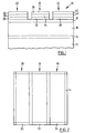
- FIG. 1 shows a cross-section of an electroluminescent device utilizing a phosphor of the present invention.
- Figure 2 shows a plan view of the electroluminescent device.
- the electroluminescent device generally indicated by 10, has a substrate 12 on which is located row electrode 14.
- Thick film dielectric 16 has thin film dielectric 18 thereon.
- Thin film dielectric 18 is shown with three pixel columns, referred to as 20, 22 and 24, located thereon.
- the pixel columns contain phosphors to provide the three basic colours viz. red, green and blue.
- Pixel column 20 has red phosphor 26 located in contact with thin film dielectric 18.
- Another thin film dielectric 28 is located on red phosphor 26, and column electrode 30 is located on thin film dielectric 28.
- pixel column 22 has green phosphor 32 on thin film dielectric 18, with thin film dielectric 34 and column electrode 36 thereon.
- Pixel column 24 has blue phosphor 38 on thin film dielectric 18, with thin film dielectric 40 and column electrode 42 thereon.
- electroluminescent device 10 does not have an optical filter associated with the blue phosphor 42.
- blue phosphor 42 is a phosphor of the invention and is as described herein.
- the phosphor of the present invention provides a high luminosity blue emission that does not require an optical filter in order to achieve improved and acceptable colour coordinates for the blue sub-pixel element of a full colour electroluminescent display.
- the blue sub-pixel pixel performance is believed to meet the luminosity and colour temperature specifications for current generation cathode ray tube displays
- a magnesium barium thioaluminate phosphor film was formed on a thick film substrate and annealed at a temperature of about 850°C.
- This luminosity allows for an areal blue luminosity of 30 candelas per square meter when 50% of the active area of a pixel is occupied by the blue sub-pixel.
- Areal blue luminosity is defined as the blue luminosity averaged over the nominal image area of a display.
- a series of magnesium barium thioaluminate thin film phosphors materials were prepared by blending powders of aluminum sulphide, barium sulphide, magnesium sulphide and europium sulphide in the desired ratios and making pressed pellets of the blended powders.
- the pellets were placed in an alumina boat and fired in a nitrogen atmosphere using a belt furnace, using a temperature profile such that the films were subject to a nominal peak temperature of 900°C for about 7 minutes.
- the actual sample temperature may have been lower than 900°C because of the thermal capacity of the alumina boat.
- the fired pellets with no magnesium i.e. a 0, did not show any visual changes following firing. Photoluminescence measurements on the fired pellets showed that this material was not homogenous when viewed under a magnifying glass, with different areas emitting different colours of light.
- the photoluminescence properties of the materials containing magnesium were examined, using a magnifying glass. It was found that all of the samples showed uniform blue emission. This indicates that the materials were homogeneous at the level of detail resolvable by a magnifying glass, with no evidence of a luminance-generating second phase precipitate.
- X-ray diffraction analysis of a sample of material containing magnesium showed a phase with a crystal structure very similar to barium thioaluminate but with slightly reduced lattice constants. This might be expected as a result of substitution of some barium by magnesium.
- the reduced melting temperature for the magnesium-containing materials indicates that the materials should be amenable to annealing at lower temperatures than the materials not containing magnesium, which would make them more compatible with thick film dielectric substrates.
- Magnesium barium thioaluminate materials of the formula Mg a Ba 1-a Al 2 S 4 :Eu, with a nominal value of a 0.5 and a europium concentration equal to 3 atomic percent of the sum of the magnesium and barium concentrations, were deposited as thin films on thick film dielectric structures.
- the deposition method used was dual source electron beam evaporation, in which one source was a pressed pellet of aluminum sulphide (Al 2 S 3 ) and the other source was a pressed pellet consisting of a mixture of barium sulphide, magnesium sulphide and europium sulphide.
- the phosphor films were annealed at a nominal temperature of 850°C under nitrogen.
- composition of the materials in this example is for the source materials, and the composition of the deposited films may vary from these compositions.
- the electroluminescent emission of the resultant phosphor showed the same blue shift with respect to material not containing magnesium as was observed with photoluminescence measurements.
- the luminance of the magnesium-containing phosphor was about 50 cd/m 2 at a voltage that was 50 volts above the threshold voltage of 160 volts for the fabricated electroluminescent pixel, and 90 cd/m 2 at 100 volts above the threshold voltage.
- the excitation frequency was 120 Hz.
- the luminance of a barium thioaluminate phosphor film without magnesium at the same excitation frequency, in a structure that was not identical, was about 25 to 30 cd/m 2 at 50 volts above the 190 volt threshold.
- the luminance was about 40 cd/m 2 at 70 volts above the threshold voltage.
- Example III The procedure of Example III was repeated, except that europium oxide (Eu 2 O 3 ) was used instead of europium sulphide.
- the remaining compounds were aluminum sulphide, barium sulphide and magnesium sulphide, as in Example III.
- the nominal value of a in the formula of Example III was 0.5.
- the europium concentration was 3 atomic percent of the sum of the magnesium and barium concentrations.
- the resultant phosphor had the same characteristics as the phosphor of Example III that had been formed using europium sulphide. It is therefore believed that europium sulphide may be replaced in whole or in part with europium oxide for europium concentrations of up to 3 atomic percent.
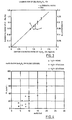
- This example illustrates the ability to control the elemental composition of a magnesium barium thioaluminate phosphor film deposited on a thick film dielectric structure using the method described in Example II. This example also shows the dependence on elemental composition of the colour coordinates of the light emission from the resulting electroluminescent element.
- Two source pellets were used to deposit the phosphor film viz. aluminum sulphide and europium doped magnesium-barium sulphide.
- the deposition rate of aluminum sulphide relative to that for the europium-doped magnesium-barium sulphide was controlled by varying the electron beam power for the aluminum sulphide source pellet.
- the deposition rates of the two source materials were monitored using independent rate monitors.
- the composition of the deposited films was measured using secondary ion mass spectroscopy (SIMS).
- Fig. 3 shows the ratio of aluminum to the combined alkaline earth peaks i.e. the sum of the magnesium and barium peaks, observed in the SIMS spectrum plotted against the relative atomic deposition rate ratio for the two source materials.
- the ratio of aluminum to alkaline earth elements in the phosphor film is proportional to the relative deposition rates of the source materials.
- Figure 3 also shows the y colour coordinate of the electroluminescent emission for the phosphor materials as a function of the elemental composition. It is evident over the range evaluated that the y coordinate is not very sensitive to the elemental composition, although a tendency to a somewhat higher value is noted for the sample with the lowest aluminum concentration. The observed variation may be due, however, to other variables inherent in the materials and processes used in the fabrication of the pixel used. Although not shown, the x colour coordinate and the luminance also did not show any systematic dependence on the elemental composition over the range evaluated.
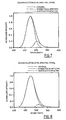
- the europium concentration was varied so that the atomic ratio of europium to barium was in the range of 4 to 25 percent.
- the films were deposited in an atmosphere of up to 0.2 milliTorr (0.266 Pascals) of hydrogen sulphide.
- the photoluminescence of the films when they were irradiated with 365 nm ultraviolet light was found to increase in an approximately linear manner for up to 20 atomic percent europium and then decrease at a higher concentration of 25 percent europium, as shown in Figure 4.
- the data indicates a change in the photoluminescence properties as the europium concentration is increased above 20 atomic percent, although it cannot be concluded from this example that this change is directly related to the increase in the europium concentration.
- Powders to form magnesium barium thioaluminate were prepared according to the method used in Example II, except that the powders were annealed at a temperature of 1000°C under nitrogen for 10 minutes, rather than at 900°C.
- the fraction "a" of barium replaced by magnesium in the formula Mg a Ba 1-a Al 2 S 4 :Eu was varied over the range 0.10, 0.30 0.50, 0.70 and 0.90.
- the sample with a 0.9 was observed to consist of at least two crystal phases that respectively emitted green and blue light under 365 nm ultraviolet excitation.
- the CIE x-coordinate for the photoluminescence was 0.14, independent of the value of "a”.
- the phase having a crystal structure very close to that of barium thioaluminate (“the barium thioaluminate-like phase”) may have a lattice constant slightly smaller than that for pure barium thioaluminate, possibly due to the substitution of some barium in the crystal lattice by magnesium.
- the crystal differs from that of manganese thioaluminate in that an XRD peak is present corresponding to a crystal lattice spacing of 11.99 Angstroms that possibly corresponds to a superlattice distortion relative to a manganese thioaluminate structure.
- the sample with a 0.7 showed the manganese thioaluminate-like phase with the 11.99 Angstrom peak as being the dominant phase, but with additional phases present including the barium thioaluminate-like phase and minor quantities of several phases not found in the samples with lower values of "a".
- this sample appears to the only one that is comprised largely of a single crystal structure.
- An essentially single phase phosphor film in an electroluminescent display may be beneficial, as electrons injected into the phosphor film may have a reduced tendency to scatter from grain boundaries between different crystal phases and therefore have less tendency to lose energy in a manner that doesn't cause the emission of useful light. This would increase the electrical-to-light energy conversion efficiency of the display.
- the additional phases are consistent with the presence of a short wavelength secondary emission peak in the PL spectra.
- There is also a slight shift of the main PL peak towards longer wavelength which indicates a variability in the atomic environment of the europium activator in the main phase as the nominal composition is varied. This might indicate a range for the elemental composition of the main phase.
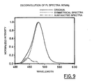
- the photoluminescence spectra of the samples under 365 nm excitation was also recorded. In order to try to determine whether or not small emission peaks were masked by the main emission peak, the spectra were de-convoluted. The center of the emission peaks was selected. A mirror image of the half of the emission peak that decreased most steeply in amplitude from the center was reflected about the centre of the peak, and the thus constructed symmetrical peak was subtracted from the measured emission peak.
- the resultant deconvoluted peak revealed the presence of small peaks shifted in wavelength from the main peak.
- results obtained correlate well with the XRD results, which indicate the presence of a barium thioaluminate-like phase for low values of "a” and a multiplicity of other distinct phases for "a” near 0.9.
- results also correlate with the visible multi-colour light emission from the sample with "a” about equal to 0.9 when the sample is under ultraviolet emission.
Landscapes
- Chemical & Material Sciences (AREA)
- Engineering & Computer Science (AREA)
- Materials Engineering (AREA)
- Organic Chemistry (AREA)
- Inorganic Chemistry (AREA)
- Chemical Kinetics & Catalysis (AREA)
- Mechanical Engineering (AREA)
- Metallurgy (AREA)
- Luminescent Compositions (AREA)
- Electroluminescent Light Sources (AREA)
- Physical Vapour Deposition (AREA)
- Compounds Of Alkaline-Earth Elements, Aluminum Or Rare-Earth Metals (AREA)
Applications Claiming Priority (5)
| Application Number | Priority Date | Filing Date | Title |
|---|---|---|---|
| US23254900P | 2000-09-14 | 2000-09-14 | |
| US232549P | 2000-09-14 | ||
| US09/798,203 US20020122895A1 (en) | 2000-09-14 | 2001-03-02 | Magnesium barium thioaluminate and related phosphor materials |
| US798203 | 2001-03-02 | ||
| PCT/CA2001/001234 WO2002023957A1 (en) | 2000-09-14 | 2001-08-30 | Magnesium barium thioaluminate and related phosphor materials |
Publications (2)
| Publication Number | Publication Date |
|---|---|
| EP1323337A1 EP1323337A1 (en) | 2003-07-02 |
| EP1323337B1 true EP1323337B1 (en) | 2005-11-09 |
Family
ID=26926110
Family Applications (1)
| Application Number | Title | Priority Date | Filing Date |
|---|---|---|---|
| EP01966898A Expired - Lifetime EP1323337B1 (en) | 2000-09-14 | 2001-08-30 | Magnesium barium thioaluminate and related phosphor materials |
Country Status (8)
| Country | Link |
|---|---|
| US (2) | US20020122895A1 (enExample) |
| EP (1) | EP1323337B1 (enExample) |
| JP (1) | JP5073148B2 (enExample) |
| AT (1) | ATE309689T1 (enExample) |
| AU (1) | AU2001287442A1 (enExample) |
| CA (1) | CA2421171C (enExample) |
| DE (1) | DE60114867T2 (enExample) |
| WO (1) | WO2002023957A1 (enExample) |
Families Citing this family (24)
| Publication number | Priority date | Publication date | Assignee | Title |
|---|---|---|---|---|
| US20020145129A1 (en) * | 1998-08-14 | 2002-10-10 | Yun Sun-Jin | High luminance-phosphor and method for fabricating the same |
| JP3479273B2 (ja) | 2000-09-21 | 2003-12-15 | Tdk株式会社 | 蛍光体薄膜その製造方法およびelパネル |
| US6617782B2 (en) * | 2001-05-30 | 2003-09-09 | Ifire Technology Inc. | Thioaluminate phosphor material with a gadolinium co-activator |
| US6686062B2 (en) | 2001-06-13 | 2004-02-03 | Ifire Technology Inc. | Magnesium calcium thioaluminate phosphor |
| US6793782B2 (en) * | 2001-12-21 | 2004-09-21 | Ifire Technology Inc. | Sputter deposition process for electroluminescent phosphors |
| JP2003301171A (ja) * | 2002-02-06 | 2003-10-21 | Tdk Corp | 蛍光体薄膜、その製造方法およびelパネル |
| CA2495771A1 (en) * | 2002-09-12 | 2004-03-25 | Ifire Technology Corp. | Silicon oxynitride passivated rare earth activated thioaluminate phosphors for electroluminescent displays |
| DE60324577D1 (de) * | 2002-09-13 | 2008-12-18 | Ifire Ip Corp | Dünnfilmleuchtstoff für elektrolumineszenzanzeigen |
| KR101082130B1 (ko) * | 2002-10-18 | 2011-11-09 | 이화이어 아이피 코포레이션 | 컬러 전계발광 디스플레이 |
| JP2006511045A (ja) | 2002-12-20 | 2006-03-30 | アイファイアー・テクノロジー・コープ | 厚膜誘電性エレクトロルミネッセンスディスプレイ用のバリア層 |
| TW200420740A (en) * | 2003-01-30 | 2004-10-16 | Ifire Technology Inc | Controlled sulfur species deposition process |
| JP4263001B2 (ja) | 2003-03-06 | 2009-05-13 | アイファイヤー アイピー コーポレイション | スパッタリングターゲット |
| WO2004112437A1 (en) * | 2003-06-13 | 2004-12-23 | Matsushita Electric Industrial Co., Ltd. | Luminescent device, display device, and display device control method |
| WO2005003402A2 (en) * | 2003-07-03 | 2005-01-13 | Ifire Technology Corp. | Hydrogen sulfide injection method for phosphor deposition |
| US8057856B2 (en) | 2004-03-15 | 2011-11-15 | Ifire Ip Corporation | Method for gettering oxygen and water during vacuum deposition of sulfide films |
| JP4831939B2 (ja) * | 2004-03-31 | 2011-12-07 | アイファイヤー アイピー コーポレイション | 発光体薄膜及び発光素子 |
| US7427367B2 (en) * | 2004-08-06 | 2008-09-23 | Ifire Technology Corp. | Barium thioaluminate phosphor materials with novel crystal structures |
| US7790003B2 (en) * | 2004-10-12 | 2010-09-07 | Southwest Research Institute | Method for magnetron sputter deposition |
| US7592051B2 (en) * | 2005-02-09 | 2009-09-22 | Southwest Research Institute | Nanostructured low-Cr Cu-Cr coatings for high temperature oxidation resistance |
| JP2007056235A (ja) | 2005-07-28 | 2007-03-08 | Sony Corp | 蛍光体、光学装置、及び表示装置 |
| KR100835069B1 (ko) * | 2007-01-02 | 2008-06-03 | 삼성전기주식회사 | 형광체 및 이를 이용한 발광장치 |
| JP2011199174A (ja) * | 2010-03-23 | 2011-10-06 | Fujifilm Corp | 発光層形成用固形材料、並びに有機電界発光素子及びその製造方法 |
| US8977735B2 (en) * | 2011-12-12 | 2015-03-10 | Rackspace Us, Inc. | Providing a database as a service in a multi-tenant environment |
| CN117602589A (zh) * | 2023-09-29 | 2024-02-27 | 中国科学院新疆理化技术研究所 | 化合物硒镓镁钙和硒镓镁钙红外非线性光学晶体及制备方法和应用 |
Family Cites Families (15)
| Publication number | Priority date | Publication date | Assignee | Title |
|---|---|---|---|---|
| US3742277A (en) * | 1971-03-18 | 1973-06-26 | Gte Laboratories Inc | Flying spot scanner having screen of strontium thiogallte coactivatedby trivalent cerium and divalent lead |
| FR2444073A1 (fr) * | 1978-12-15 | 1980-07-11 | Rhone Poulenc Ind | Nouvelles substances luminescentes a base de thiogallates d'alcalino terreux et leur procede d'invention |
| US5309070A (en) * | 1991-03-12 | 1994-05-03 | Sun Sey Shing | AC TFEL device having blue light emitting thiogallate phosphor |
| US5432015A (en) * | 1992-05-08 | 1995-07-11 | Westaim Technologies, Inc. | Electroluminescent laminate with thick film dielectric |
| JP2840185B2 (ja) * | 1993-10-21 | 1998-12-24 | 松下電器産業株式会社 | 蛍光体薄膜とこれを用いた薄膜elパネル |
| US5505986A (en) * | 1994-02-14 | 1996-04-09 | Planar Systems, Inc. | Multi-source reactive deposition process for the preparation of blue light emitting phosphor layers for AC TFEL devices |
| US5598059A (en) * | 1994-04-28 | 1997-01-28 | Planar Systems, Inc. | AC TFEL device having a white light emitting multilayer phosphor |
| JPH08134440A (ja) | 1994-11-14 | 1996-05-28 | Mitsui Mining & Smelting Co Ltd | 薄膜エレクトロルミネッセンス素子 |
| US5834053A (en) * | 1994-11-30 | 1998-11-10 | The Regents Of The University Of California | Blue light emitting thiogallate phosphor |
| JP2803631B2 (ja) * | 1995-07-03 | 1998-09-24 | 株式会社デンソー | エレクトロルミネッセンス素子およびその製造方法 |
| US5581150A (en) * | 1995-10-13 | 1996-12-03 | Planar Systems, Inc. | TFEL device with injection layer |
| US5656888A (en) * | 1995-11-13 | 1997-08-12 | Sun; Sey-Shing | Oxygen-doped thiogallate phosphor |
| JPH10130638A (ja) * | 1996-11-01 | 1998-05-19 | Toray Ind Inc | 蛍光体ペーストおよびそれを用いたプラズマディスプレイパネルの製造方法 |
| JP3936479B2 (ja) * | 1998-10-23 | 2007-06-27 | 三井金属鉱業株式会社 | 薄膜エレクトロルミネッセンス材料 |
| US6686062B2 (en) * | 2001-06-13 | 2004-02-03 | Ifire Technology Inc. | Magnesium calcium thioaluminate phosphor |
-
2001
- 2001-03-02 US US09/798,203 patent/US20020122895A1/en not_active Abandoned
- 2001-08-30 EP EP01966898A patent/EP1323337B1/en not_active Expired - Lifetime
- 2001-08-30 AT AT01966898T patent/ATE309689T1/de not_active IP Right Cessation
- 2001-08-30 AU AU2001287442A patent/AU2001287442A1/en not_active Abandoned
- 2001-08-30 DE DE60114867T patent/DE60114867T2/de not_active Expired - Lifetime
- 2001-08-30 JP JP2002526805A patent/JP5073148B2/ja not_active Expired - Fee Related
- 2001-08-30 CA CA002421171A patent/CA2421171C/en not_active Expired - Fee Related
- 2001-08-30 WO PCT/CA2001/001234 patent/WO2002023957A1/en not_active Ceased
-
2003
- 2003-05-20 US US10/441,872 patent/US6919682B2/en not_active Expired - Lifetime
Also Published As
| Publication number | Publication date |
|---|---|
| CA2421171A1 (en) | 2002-03-21 |
| WO2002023957A1 (en) | 2002-03-21 |
| EP1323337A1 (en) | 2003-07-02 |
| US20040027048A1 (en) | 2004-02-12 |
| JP2004524378A (ja) | 2004-08-12 |
| CA2421171C (en) | 2008-11-18 |
| AU2001287442A1 (en) | 2002-03-26 |
| DE60114867T2 (de) | 2006-05-24 |
| US6919682B2 (en) | 2005-07-19 |
| ATE309689T1 (de) | 2005-11-15 |
| JP5073148B2 (ja) | 2012-11-14 |
| DE60114867D1 (de) | 2005-12-15 |
| US20020122895A1 (en) | 2002-09-05 |
Similar Documents
| Publication | Publication Date | Title |
|---|---|---|
| EP1323337B1 (en) | Magnesium barium thioaluminate and related phosphor materials | |
| US6610352B2 (en) | Multiple source deposition process | |
| US7582228B2 (en) | Barium thioaluminate phosphor materials with novel crystal structures | |
| US6841045B2 (en) | Single source sputtering of thioaluminate phosphor films | |
| JP2004528465A (ja) | ガドリニウム活性化共役因子を含むチオアルミネート蛍光体材料 | |
| JP4247315B2 (ja) | マグネシウムカルシウムチオアルミネート蛍光体 | |
| WO2006108291A1 (en) | Magnesium oxide-containing barrier layer for thick dielectric electroluminescent displays | |
| TWI233453B (en) | Multiple source deposition process |
Legal Events
| Date | Code | Title | Description |
|---|---|---|---|
| PUAI | Public reference made under article 153(3) epc to a published international application that has entered the european phase |
Free format text: ORIGINAL CODE: 0009012 |
|
| 17P | Request for examination filed |
Effective date: 20030312 |
|
| AK | Designated contracting states |
Designated state(s): AT BE CH CY DE DK ES FI FR GB GR IE IT LI LU MC NL PT SE TR |
|
| AX | Request for extension of the european patent |
Extension state: AL LT LV MK RO SI |
|
| RAP1 | Party data changed (applicant data changed or rights of an application transferred) |
Owner name: IFIRE TECHNOLOGY CORP. |
|
| GRAP | Despatch of communication of intention to grant a patent |
Free format text: ORIGINAL CODE: EPIDOSNIGR1 |
|
| GRAS | Grant fee paid |
Free format text: ORIGINAL CODE: EPIDOSNIGR3 |
|
| GRAA | (expected) grant |
Free format text: ORIGINAL CODE: 0009210 |
|
| AK | Designated contracting states |
Kind code of ref document: B1 Designated state(s): AT BE CH CY DE DK ES FI FR GB GR IE IT LI LU MC NL PT SE TR |
|
| PG25 | Lapsed in a contracting state [announced via postgrant information from national office to epo] |
Ref country code: IT Free format text: LAPSE BECAUSE OF FAILURE TO SUBMIT A TRANSLATION OF THE DESCRIPTION OR TO PAY THE FEE WITHIN THE PRESCRIBED TIME-LIMIT;WARNING: LAPSES OF ITALIAN PATENTS WITH EFFECTIVE DATE BEFORE 2007 MAY HAVE OCCURRED AT ANY TIME BEFORE 2007. THE CORRECT EFFECTIVE DATE MAY BE DIFFERENT FROM THE ONE RECORDED. Effective date: 20051109 Ref country code: CH Free format text: LAPSE BECAUSE OF FAILURE TO SUBMIT A TRANSLATION OF THE DESCRIPTION OR TO PAY THE FEE WITHIN THE PRESCRIBED TIME-LIMIT Effective date: 20051109 Ref country code: BE Free format text: LAPSE BECAUSE OF FAILURE TO SUBMIT A TRANSLATION OF THE DESCRIPTION OR TO PAY THE FEE WITHIN THE PRESCRIBED TIME-LIMIT Effective date: 20051109 Ref country code: LI Free format text: LAPSE BECAUSE OF FAILURE TO SUBMIT A TRANSLATION OF THE DESCRIPTION OR TO PAY THE FEE WITHIN THE PRESCRIBED TIME-LIMIT Effective date: 20051109 Ref country code: FI Free format text: LAPSE BECAUSE OF FAILURE TO SUBMIT A TRANSLATION OF THE DESCRIPTION OR TO PAY THE FEE WITHIN THE PRESCRIBED TIME-LIMIT Effective date: 20051109 Ref country code: AT Free format text: LAPSE BECAUSE OF FAILURE TO SUBMIT A TRANSLATION OF THE DESCRIPTION OR TO PAY THE FEE WITHIN THE PRESCRIBED TIME-LIMIT Effective date: 20051109 Ref country code: NL Free format text: LAPSE BECAUSE OF FAILURE TO SUBMIT A TRANSLATION OF THE DESCRIPTION OR TO PAY THE FEE WITHIN THE PRESCRIBED TIME-LIMIT Effective date: 20051109 |
|
| REG | Reference to a national code |
Ref country code: GB Ref legal event code: FG4D |
|
| REG | Reference to a national code |
Ref country code: CH Ref legal event code: EP |
|
| REG | Reference to a national code |
Ref country code: IE Ref legal event code: FG4D |
|
| REF | Corresponds to: |
Ref document number: 60114867 Country of ref document: DE Date of ref document: 20051215 Kind code of ref document: P |
|
| PG25 | Lapsed in a contracting state [announced via postgrant information from national office to epo] |
Ref country code: GR Free format text: LAPSE BECAUSE OF FAILURE TO SUBMIT A TRANSLATION OF THE DESCRIPTION OR TO PAY THE FEE WITHIN THE PRESCRIBED TIME-LIMIT Effective date: 20060209 Ref country code: DK Free format text: LAPSE BECAUSE OF FAILURE TO SUBMIT A TRANSLATION OF THE DESCRIPTION OR TO PAY THE FEE WITHIN THE PRESCRIBED TIME-LIMIT Effective date: 20060209 Ref country code: SE Free format text: LAPSE BECAUSE OF FAILURE TO SUBMIT A TRANSLATION OF THE DESCRIPTION OR TO PAY THE FEE WITHIN THE PRESCRIBED TIME-LIMIT Effective date: 20060209 |
|
| PG25 | Lapsed in a contracting state [announced via postgrant information from national office to epo] |
Ref country code: ES Free format text: LAPSE BECAUSE OF FAILURE TO SUBMIT A TRANSLATION OF THE DESCRIPTION OR TO PAY THE FEE WITHIN THE PRESCRIBED TIME-LIMIT Effective date: 20060220 |
|
| PG25 | Lapsed in a contracting state [announced via postgrant information from national office to epo] |
Ref country code: PT Free format text: LAPSE BECAUSE OF FAILURE TO SUBMIT A TRANSLATION OF THE DESCRIPTION OR TO PAY THE FEE WITHIN THE PRESCRIBED TIME-LIMIT Effective date: 20060410 |
|
| NLV1 | Nl: lapsed or annulled due to failure to fulfill the requirements of art. 29p and 29m of the patents act | ||
| REG | Reference to a national code |
Ref country code: CH Ref legal event code: PL |
|
| ET | Fr: translation filed | ||
| PG25 | Lapsed in a contracting state [announced via postgrant information from national office to epo] |
Ref country code: IE Free format text: LAPSE BECAUSE OF NON-PAYMENT OF DUE FEES Effective date: 20060830 |
|
| PG25 | Lapsed in a contracting state [announced via postgrant information from national office to epo] |
Ref country code: MC Free format text: LAPSE BECAUSE OF NON-PAYMENT OF DUE FEES Effective date: 20060831 |
|
| PLBE | No opposition filed within time limit |
Free format text: ORIGINAL CODE: 0009261 |
|
| STAA | Information on the status of an ep patent application or granted ep patent |
Free format text: STATUS: NO OPPOSITION FILED WITHIN TIME LIMIT |
|
| 26N | No opposition filed |
Effective date: 20060810 |
|
| REG | Reference to a national code |
Ref country code: IE Ref legal event code: MM4A |
|
| REG | Reference to a national code |
Ref country code: GB Ref legal event code: 732E |
|
| REG | Reference to a national code |
Ref country code: FR Ref legal event code: TP |
|
| PG25 | Lapsed in a contracting state [announced via postgrant information from national office to epo] |
Ref country code: LU Free format text: LAPSE BECAUSE OF NON-PAYMENT OF DUE FEES Effective date: 20060830 Ref country code: TR Free format text: LAPSE BECAUSE OF FAILURE TO SUBMIT A TRANSLATION OF THE DESCRIPTION OR TO PAY THE FEE WITHIN THE PRESCRIBED TIME-LIMIT Effective date: 20051109 |
|
| PG25 | Lapsed in a contracting state [announced via postgrant information from national office to epo] |
Ref country code: CY Free format text: LAPSE BECAUSE OF FAILURE TO SUBMIT A TRANSLATION OF THE DESCRIPTION OR TO PAY THE FEE WITHIN THE PRESCRIBED TIME-LIMIT Effective date: 20051109 |
|
| PGFP | Annual fee paid to national office [announced via postgrant information from national office to epo] |
Ref country code: FR Payment date: 20090723 Year of fee payment: 9 |
|
| PGFP | Annual fee paid to national office [announced via postgrant information from national office to epo] |
Ref country code: DE Payment date: 20090824 Year of fee payment: 9 |
|
| REG | Reference to a national code |
Ref country code: FR Ref legal event code: ST Effective date: 20110502 |
|
| REG | Reference to a national code |
Ref country code: DE Ref legal event code: R119 Ref document number: 60114867 Country of ref document: DE Effective date: 20110301 |
|
| PG25 | Lapsed in a contracting state [announced via postgrant information from national office to epo] |
Ref country code: DE Free format text: LAPSE BECAUSE OF NON-PAYMENT OF DUE FEES Effective date: 20110301 Ref country code: FR Free format text: LAPSE BECAUSE OF NON-PAYMENT OF DUE FEES Effective date: 20100831 |
|
| PGFP | Annual fee paid to national office [announced via postgrant information from national office to epo] |
Ref country code: GB Payment date: 20150820 Year of fee payment: 15 |
|
| GBPC | Gb: european patent ceased through non-payment of renewal fee |
Effective date: 20160830 |
|
| PG25 | Lapsed in a contracting state [announced via postgrant information from national office to epo] |
Ref country code: GB Free format text: LAPSE BECAUSE OF NON-PAYMENT OF DUE FEES Effective date: 20160830 |