EP1306893A1 - Plasma processing apparatus - Google Patents
Plasma processing apparatus Download PDFInfo
- Publication number
- EP1306893A1 EP1306893A1 EP01949933A EP01949933A EP1306893A1 EP 1306893 A1 EP1306893 A1 EP 1306893A1 EP 01949933 A EP01949933 A EP 01949933A EP 01949933 A EP01949933 A EP 01949933A EP 1306893 A1 EP1306893 A1 EP 1306893A1
- Authority
- EP
- European Patent Office
- Prior art keywords
- plasma
- antenna
- dielectric member
- conductive plate
- processing apparatus
- Prior art date
- Legal status (The legal status is an assumption and is not a legal conclusion. Google has not performed a legal analysis and makes no representation as to the accuracy of the status listed.)
- Granted
Links
Images






Classifications
-
- H—ELECTRICITY
- H01—ELECTRIC ELEMENTS
- H01J—ELECTRIC DISCHARGE TUBES OR DISCHARGE LAMPS
- H01J37/00—Discharge tubes with provision for introducing objects or material to be exposed to the discharge, e.g. for the purpose of examination or processing thereof
- H01J37/32—Gas-filled discharge tubes
- H01J37/32009—Arrangements for generation of plasma specially adapted for examination or treatment of objects, e.g. plasma sources
- H01J37/32192—Microwave generated discharge
-
- H—ELECTRICITY
- H10—SEMICONDUCTOR DEVICES; ELECTRIC SOLID-STATE DEVICES NOT OTHERWISE PROVIDED FOR
- H10P—GENERIC PROCESSES OR APPARATUS FOR THE MANUFACTURE OR TREATMENT OF DEVICES COVERED BY CLASS H10
- H10P50/00—Etching of wafers, substrates or parts of devices
- H10P50/20—Dry etching; Plasma etching; Reactive-ion etching
- H10P50/24—Dry etching; Plasma etching; Reactive-ion etching of semiconductor materials
- H10P50/242—Dry etching; Plasma etching; Reactive-ion etching of semiconductor materials of Group IV materials
-
- B—PERFORMING OPERATIONS; TRANSPORTING
- B01—PHYSICAL OR CHEMICAL PROCESSES OR APPARATUS IN GENERAL
- B01J—CHEMICAL OR PHYSICAL PROCESSES, e.g. CATALYSIS OR COLLOID CHEMISTRY; THEIR RELEVANT APPARATUS
- B01J19/00—Chemical, physical or physico-chemical processes in general; Their relevant apparatus
- B01J19/08—Processes employing the direct application of electric or wave energy, or particle radiation; Apparatus therefor
- B01J19/087—Processes employing the direct application of electric or wave energy, or particle radiation; Apparatus therefor employing electric or magnetic energy
- B01J19/088—Processes employing the direct application of electric or wave energy, or particle radiation; Apparatus therefor employing electric or magnetic energy giving rise to electric discharges
-
- C—CHEMISTRY; METALLURGY
- C23—COATING METALLIC MATERIAL; COATING MATERIAL WITH METALLIC MATERIAL; CHEMICAL SURFACE TREATMENT; DIFFUSION TREATMENT OF METALLIC MATERIAL; COATING BY VACUUM EVAPORATION, BY SPUTTERING, BY ION IMPLANTATION OR BY CHEMICAL VAPOUR DEPOSITION, IN GENERAL; INHIBITING CORROSION OF METALLIC MATERIAL OR INCRUSTATION IN GENERAL
- C23C—COATING METALLIC MATERIAL; COATING MATERIAL WITH METALLIC MATERIAL; SURFACE TREATMENT OF METALLIC MATERIAL BY DIFFUSION INTO THE SURFACE, BY CHEMICAL CONVERSION OR SUBSTITUTION; COATING BY VACUUM EVAPORATION, BY SPUTTERING, BY ION IMPLANTATION OR BY CHEMICAL VAPOUR DEPOSITION, IN GENERAL
- C23C16/00—Chemical coating by decomposition of gaseous compounds, without leaving reaction products of surface material in the coating, i.e. chemical vapour deposition [CVD] processes
- C23C16/22—Chemical coating by decomposition of gaseous compounds, without leaving reaction products of surface material in the coating, i.e. chemical vapour deposition [CVD] processes characterised by the deposition of inorganic material, other than metallic material
- C23C16/24—Deposition of silicon only
-
- C—CHEMISTRY; METALLURGY
- C23—COATING METALLIC MATERIAL; COATING MATERIAL WITH METALLIC MATERIAL; CHEMICAL SURFACE TREATMENT; DIFFUSION TREATMENT OF METALLIC MATERIAL; COATING BY VACUUM EVAPORATION, BY SPUTTERING, BY ION IMPLANTATION OR BY CHEMICAL VAPOUR DEPOSITION, IN GENERAL; INHIBITING CORROSION OF METALLIC MATERIAL OR INCRUSTATION IN GENERAL
- C23C—COATING METALLIC MATERIAL; COATING MATERIAL WITH METALLIC MATERIAL; SURFACE TREATMENT OF METALLIC MATERIAL BY DIFFUSION INTO THE SURFACE, BY CHEMICAL CONVERSION OR SUBSTITUTION; COATING BY VACUUM EVAPORATION, BY SPUTTERING, BY ION IMPLANTATION OR BY CHEMICAL VAPOUR DEPOSITION, IN GENERAL
- C23C16/00—Chemical coating by decomposition of gaseous compounds, without leaving reaction products of surface material in the coating, i.e. chemical vapour deposition [CVD] processes
- C23C16/44—Chemical coating by decomposition of gaseous compounds, without leaving reaction products of surface material in the coating, i.e. chemical vapour deposition [CVD] processes characterised by the method of coating
- C23C16/50—Chemical coating by decomposition of gaseous compounds, without leaving reaction products of surface material in the coating, i.e. chemical vapour deposition [CVD] processes characterised by the method of coating using electric discharges
- C23C16/511—Chemical coating by decomposition of gaseous compounds, without leaving reaction products of surface material in the coating, i.e. chemical vapour deposition [CVD] processes characterised by the method of coating using electric discharges using microwave discharges
-
- B—PERFORMING OPERATIONS; TRANSPORTING
- B01—PHYSICAL OR CHEMICAL PROCESSES OR APPARATUS IN GENERAL
- B01J—CHEMICAL OR PHYSICAL PROCESSES, e.g. CATALYSIS OR COLLOID CHEMISTRY; THEIR RELEVANT APPARATUS
- B01J2219/00—Chemical, physical or physico-chemical processes in general; Their relevant apparatus
- B01J2219/08—Processes employing the direct application of electric or wave energy, or particle radiation; Apparatus therefor
- B01J2219/0894—Processes carried out in the presence of a plasma
Definitions
- the present invention relates to a plasma processing apparatus which performs a predetermined process by generating a plasma with an RF electromagnetic field.
- plasma processing apparatuses are used often to perform processes such as formation of an oxide film, crystal growth of a semiconductor layer, etching, and ashing.
- an RF plasma processing apparatus is available which can stably generate a plasma even under a comparatively low pressure.
- the RF plasma processing apparatus generates a high-density plasma by introducing an RF electromagnetic field into a processing vessel through a planar antenna.
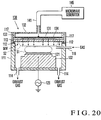
- Fig. 20 is a view showing the arrangement of an etching apparatus using a conventional RF plasma processing apparatus. Fig. 20 shows the sectional structure of part of the arrangement.
- a dielectric plate 113 is horizontally arranged in the upper opening of a cylindrical processing vessel 111.
- a seal member 112 is disposed at the bonding portion between the processing vessel 111 and dielectric plate 113 so that the hermeticity in the processing vessel 111 is ensured.
- Vacuum exhausting exhaust ports 114 are formed in the bottom of the processing vessel 111.
- a gas supply nozzle 116 is formed in the side wall of the processing vessel 111.
- the processing vessel 111 accommodates a susceptor 122 on which a substrate 121 as an etching target is to be placed. An RF voltage is applied to the susceptor 122 from an RF power supply 126.
- a radial antenna 130 is disposed on the dielectric plate 113 to supply a microwave MW into the processing vessel 111 as an RF electromagnetic field.
- the dielectric plate 113 and radial antenna 130 are covered by a seal material 117.
- the radial antenna 130 is formed of two parallel conductive plates 131 and 132 which form a radial waveguide, and a ring member 133 which closes the edges of the conductive plates 131 and 132.
- the conductive plate 131 constituting the radiation surface of the microwave MW has a large number of slots 134.
- the radial antenna 130 is connected to a microwave generator 145 through a waveguide 141.
- the interior of the processing vessel 111 is set to a predetermined vacuum degree, and after that a gas mixture of, e.g., CF 4 and Ar, is supplied from the nozzle 116 under flow rate control.
- a gas mixture of, e.g., CF 4 and Ar is supplied from the nozzle 116 under flow rate control.
- the microwave generator 145 supplies the microwave MW to the radial antenna 130 through the waveguide 141.
- the microwave MW supplied to the radial antenna 130 is radiated from the large number of slots 134 formed in the conductive plate 131 while propagating in the radial waveguide.
- the conductive plate 131 is a horizontally arranged flat plate, the microwave MW is radiated in the vertical direction.
- the microwave MW is transmitted through the dielectric plate 113 and introduced into the processing vessel 111.
- the microwave MW introduced into the processing vessel 111 ionizes the gas in the processing vessel 111 to generate a plasma in a space S1 above the substrate 121 as the processing target.
- the microwave MW introduced into the processing vessel 111 is not entirely absorbed directly by plasma generation. That microwave MW which is not absorbed but is left repeats reflection in the processing vessel 111 to form a standing wave in a space S2 between the radial antenna 130 and plasma generating space S1.
- the microwave MW which forms the standing wave is also known to contribute to plasma generation.
- the ions of the plasma generated in this manner are extracted by the negative potential of the susceptor 122 and utilized for the etching process.
- the present invention has been made to solve the above problems, and has as its object to improve the distribution of the plasma generated by an RF electromagnetic field.
- a plasma processing apparatus is characterized in that at least one of a first conductive plate constituting the radiation surface of a slot antenna and a second conductive plate opposed to the first conductive plate inclines relative to a first dielectric member opposed to the radiation surface of the slot antenna.
- a radial antenna, a cavity antenna, or the like can be used as the slot antenna.
- the electromagnetic field from the slot antenna enters in a direction inclining with respect to the direction of normal to the first dielectric member.
- a plasma plane opposing the first dielectric member forms a shape conforming to the first dielectric member.
- a change in electric field of the electromagnetic field since the boundary between the plasma and the first dielectric member and a point where the plasma density reaches a cutoff density will be briefly described.
- the strength of a component in a direction parallel to the plasma plane maintains a substantially constant value, while the strength of a component in the direction of normal to the plasma plane increases monotonously. Therefore, when the electromagnetic field enters in a direction inclining with respect to the direction of normal to the plasma plane, the strength of the electric field as the synthesis of the two components can be increased more when compared to a case wherein the electromagnetic field enters in the direction of normal to the plasma plane. As a result, the plasma generating efficiency of the electric field of the electromagnetic field entering directly from the slot antenna can be improved.
- the space between the first conductive plate and the plasma plane deforms. Accordingly, the standing wave mode changes, so the plasma generation distribution changes.
- the space in the antenna has a distribution. Therefore, when the distribution of the characteristic impedance of the antenna is adjusted and the distribution of the radiation amount of the antenna is adjusted, the plasma generation distribution is adjusted.
- the first and second conductive plates of the slot antenna, and the first dielectric member have a common central axis, and may have stereoscopic shapes each symmetrical with respect to this central axis.
- the sectional shapes obtained by cutting each stereoscopic shape at any plane including the central axis may be symmetrical with respect to the central axis.
- At least one of the first and second conductive plates and first dielectric member may have an upward convex shape or downward convex shape, so that the first and second conductive plates of the slot antenna incline with respect to the first dielectric member.
- a gap between the first and second conductive plates may be set to 5 mm or more and less than ⁇ g/2 where ⁇ g ( ⁇ g > 10 mm) is the wavelength of an electromagnetic field between the first and second conductive plates.
- ⁇ g ⁇ g > 10 mm
- the gap is 5 mm or more, electric discharge between the conductive plates can be prevented.
- the gap is set to less than ⁇ g/2, formation of a standing wave between the conductive plates can be prevented.
- the first dielectric member may have a flat plate-like shape or a dome-like shape.
- the first dielectric member may be constituted by a bell jar which isolates at least part of an inner surface of the processing vessel from a susceptor arranged in the processing vessel. Then, contamination occurring when the generated plasma comes into contact with the inner surface of the processing vessel to sputter it can be suppressed.
- the plasma processing apparatus may further comprise a second dielectric member arranged on a side different from the susceptor with respect to the first dielectric member and serving to form a sealed space together with the first dielectric member, and supply means for supplying a fluid in the sealed space so as to adjust a temperature of the first dielectric member.
- the second dielectric member may be arranged between the first dielectric member and the slot antenna, or midway along the feeder of the slot antenna.
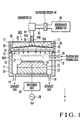
- Fig. 1 is a view showing the arrangement of an etching apparatus according to the first embodiment of the present invention.
- Fig. 1 shows the sectional structure of part of the arrangement.
- the vertical direction is defined as the Z-axis direction.
- the etching apparatus shown in Fig. 1 has a cylindrical processing vessel 11 with an upper opening.
- the processing vessel 11 is made of a conductor such as aluminum.
- a flat plate-like dielectric plate (first dielectric member) 13 is horizontally arranged in the upper opening of the processing vessel 11.
- a quartz glass or a ceramic material e.g., Al 2 O 3 or AlN
- a seal member 12 such as an O-ring is disposed at the bonding portion between the processing vessel 11 and dielectric plate 13. This assures the hermeticity in the processing vessel 11.
- Exhaust ports 14 communicating with a vacuum pump (not shown) are formed in the bottom of the processing vessel 11, so that the interior of the processing vessel 11 can be evacuated to a predetermined vacuum degree.
- a plasma gas supply nozzle 15 for introducing a plasma gas such as Ar into the processing vessel 11, and a process gas supply nozzle 16 for introducing an etching gas such as CF 4 into the processing vessel 11 are formed in the upper and lower portions, respectively, of the side wall of the processing vessel 11.
- the nozzles 15 and 16 are formed of quartz pipes or the like.
- the processing vessel 11 accommodates a susceptor 22 for placing an etching target substrate (target object) 21 on its upper surface.
- the susceptor 22 is fixed on a support table 23 which is fixed to the bottom of the processing vessel 11 through an insulating plate 24.
- the susceptor 22 is connected to a bias RF power supply 26 through a matching box 25.
- the RF power supply 26 generates a high frequency of, e.g., 2 MHz to 13.56 MHz.
- a radial antenna 30A is disposed on the dielectric plate 13 with its radiation surface (conductive plate 31 to be described later) facing down.
- the radial antenna 30A supplies a microwave MW into the processing vessel 11 as an RF electromagnetic field.
- the dielectric plate 13 is opposed to the radiation surface of the radial antenna 30A, and covers the radiation surface entirely. Hence, the radial antenna 30A is protected from a plasma generated in the processing vessel 11.
- the circumferential surfaces of the dielectric plate 13 and radial antenna 30A are covered by a shield material 17.
- the radial antenna 30A is formed of a first conductive plate 31A constituting the radiation surface, a second conductive plate 32 arranged above the conductive plate 31A to oppose it, and a ring member 33 for closing the edges of the conductive plates 31A and 32.
- the conductive plates 31A and 32, and the ring member 33 are made of a conductor such as copper or aluminum.
- a microwave inlet port 35 is formed at the center of the conductive plate 32 constituting the antenna upper surface.
- a large number of slots 34 are formed as radiating elements in the conductive plate 31A constituting the antenna lower surface.
- the two conductive plates 31A and 32 form a radial waveguide which guides the microwave MW.
- the conductive plates 31A and 32 of the radial antenna 30A, and the dielectric plate 13 have a common central axis in the Z-axis direction, and have stereoscopic shapes which are symmetrical with respect to the central axis. In other words, a sectional shape obtained by cutting each stereoscopic shape at any plane including the central axis is symmetrical with respect to the central axis.
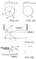
- Fig. 2 includes views showing the arrangement of the conductive plate 31A constituting the lower surface of the radial antenna 30A, in which Fig. 2(a) is a perspective view, and Fig. 2(b) is a plan view.
- the conductive plate 32 constituting the antenna upper surface is a flat plate.
- the conductive plate 31A constituting the lower surface has an upward convex circular conical surface. Accordingly, the circular conical surface of the conductive plate 31A inclines with respect to the flat plate-like dielectric plate 13. This is the characteristic feature of the etching apparatus shown in Fig. 1.
- the conductive plate 31A has a large number of concentric slots 34 extending in the circumferential direction, as shown in Fig. 2(b). Each slot 34 is formed along the direction of normal to that portion of the conductive plate 31A where it is formed.
- the length of each slit 34 and the pitch among the slots 34 which are adjacent in the radial direction are set on the basis of a wavelength (wavelength which is shortened by a delay member 39 (to be described later)) ⁇ g of the microwave MW in the radial waveguide.
- the pitch is set to about ⁇ g/20 to ⁇ g/30.
- Fig. 3 is an enlarged sectional view of the radial antenna 30A, and shows a support mechanism for the conductive plate 31A.
- the center of the conductive plate 32 is thick, and has three rectangular or circular through holes 61.
- the three through holes 61 are formed equiangularly on one circumference having the center of the conductive plate 32 as its center. Studs 62 with a sufficient length are inserted in the through holes 61.
- the conductive plate 31A is fixed to the lower surfaces of the studs 62 by fastening screws 63.
- the studs 62 fixed to the conductive plate 31A by fastening are fixed to the conductive plate 32 with nuts 64.
- the inclination of the conductive plate 31A can be set to a desired angle by adjusting the fixing positions of the nuts 64.
- those made of a dielectric such as a ceramic material can be used.
- the studs 62 may not be fixed to the conductive plate 32 with the nuts 64, but the angle of inclination of the conductive plate 31A may be changed through remote control of vertically moving the studs 62 by utilizing a driving unit such as a motor.
- the gap between the two conductive plates 31A and 32 is set to 5 mm or more and less than ⁇ g/2 where ⁇ g/2 > 10 mm.
- the gap between the conductive plates 31A and 32 is less than 6 cm.
- the gap at the vertex of the conductive plate 31A is set to 5 mm or more, and the gap at the circumference of the conductive plate 31A is set to less than 6 cm.
- the gap is set to 5 mm or more, electric discharge between the conductive plates 31A and 32 can be prevented.
- the gap is set to less than ⁇ g/2, formation of a standing wave between the conductive plates 31A and 32 can be prevented.
- the radial waveguide formed of the conductive plates 31A and 32 accommodates the delay member 39 made of a dielectric material, e.g., a ceramic material, with a relative dielectric constant larger than 1.
- the delay member 39 has a function of shortening the wavelength of the microwave MW by decreasing the propagation speed of the microwave MW it acts on.
- the delay member 39 can improve the radiation efficiency of the microwave MW of the radial antenna 30A.
- a coaxial cable 41 is connected to the center of the radial antenna 30A.
- An outer conductor 41A of the coaxial cable 41 is connected to the periphery of the microwave inlet port 35 of the conductive plate 32.
- the distal end of a central conductor 41B of the coaxial cable 41 forms a circular cone, and the bottom of the circular cone is connected to the vertex of the conductive plate 31A.
- the coaxial cable 41 connected to the radial antenna 30A in this manner is connected to a microwave generator 45 through a rectangular coaxial converter 42 and rectangular waveguide 43.
- the microwave generator 45 generates the microwave MW of, e.g., 2.45 GHz.
- the frequency of the microwave MW suffices if it falls within the range of 1 GHz to 19 GHz.
- a matching circuit 44 for matching the impedance is connected midway along the rectangular waveguide 43, so that the power use efficiency can be improved.
- the substrate 21 is placed on the upper surface of the susceptor 22, and the interior of the processing vessel 11 is set to a vacuum degree of, e.g., about 0.01 Pa to 10 Pa. While maintaining this vacuum degree, Ar is supplied as the plasma gas from the plasma gas supply nozzle 15, and an etching gas such as CF 4 is supplied from the process gas supply nozzle 16 under flow rate control.
- a vacuum degree e.g., about 0.01 Pa to 10 Pa.
- Ar is supplied as the plasma gas from the plasma gas supply nozzle 15, and an etching gas such as CF 4 is supplied from the process gas supply nozzle 16 under flow rate control.
- the microwave MW from the microwave generator 45 is supplied to the radial antenna 30A through the rectangular waveguide 43, rectangular coaxial converter 42, and coaxial cable 41.
- the microwave MW supplied to the radial antenna 30A propagates radially from the center toward the periphery of the radial waveguide formed of the conductive plates 31A and 32, and leaks little by little from the large number of slots 34 formed with a fine pitch.
- the microwave MW leaking from the radial antenna 30A is transmitted through the dielectric plate 13 and is introduced into the processing vessel 11.
- the electric field of the microwave MW ionizes Ar, thus generating a plasma in a space S1 above the substrate 11 as the processing target.
- the susceptor 22 is biased with a negative potential, so that ions are extracted from the generated plasma to etch the substrate 21.
- Fig. 4 includes views of apparatuses used for this photographing, in which Fig. 4(a) is a sectional view showing the size of the radial antenna 130 of the etching apparatus shown in Fig. 20, Fig. 4(b) is a sectional view showing the size of the radial antenna 30A of the etching apparatus shown in Fig. 1, and Fig. 4(c) shows the arrangement of a CCD camera.
- a CCD camera 29 was arranged at the center of the susceptor 22 or 122 where the substrate 21 or 121 is not placed, and the plasma generating space S1 was photographed.
- the radial antenna 130 with the size as shown in Fig. 4(a) was used. More specifically, the diameter and thickness of the conductive plate 131 were set to 480 mm and 0.8 mm, respectively, and the height of the ring member 133 was set to 15 mm.
- the radial antenna 30A with the size as shown in Fig. 4(b) was used.
- the diameter and thickness of the conductive plate 31A and the height of the ring member 33 were set to be equal to those of the radial antenna 130, while the height at the center (height of the circular conical surface) of the conductive plate 31A with reference to its circumference was set to 5 mm.
- Fig. 5 includes schematic views of images obtained when the plasmas were photographed under these conditions, in which Fig. 5(a) shows an image obtained with the etching apparatus shown in Fig. 20, and Fig. 5(b) shows an image obtained with the etching apparatus shown in Fig. 1.
- Fig. 5(a) shows an image obtained with the etching apparatus shown in Fig. 20,
- Fig. 5(b) shows an image obtained with the etching apparatus shown in Fig. 1.
- the conventional etching apparatus using the radial antenna 130 with the radial waveguide formed of parallel plates the portions 151A and 151B where the plasma was generated at a high density were observed near the center of the plasma generating region 150.
- the etching apparatus shown in Fig. 1 using the radial antenna 30A with the circular conical conductive plate 31A serving as the radiation surface as shown in Fig. 5(b)
- no portion 151A or 151B where a plasma was generated at a high density was observed in a plasma generating region
- Part of the microwave MW introduced from the radial antenna 30A into the processing vessel 11 is not absorbed by plasma generation, but forms a standing wave in a space S2 between the radial antenna 30A and plasma generating space S1, and the electric field of the standing wave contributes to plasma generation.
- This is the same as in the conventional etching apparatus. Therefore, in the etching apparatus shown in Fig. 1 as well, both the electric field of the microwave MW which has entered the plasma from the radial antenna 30A directly and the electric field of the standing wave formed in the processing vessel 11 contribute to plasma generation.
- the reason the distribution of the plasma is improved in the etching apparatus shown in Fig. 1 can be described from the following three viewpoints of (1) improvement in plasma generating efficiency of the electric field of the microwave MW which has entered directly, (2) adjustment of the distribution in the space in the radial antenna 30A, and (3) change in shape of the standing wave forming space S2.
- Fig. 6 includes conceptual graphs showing a change in density of a plasma having a plasma plane perpendicular to the Z-axis direction (vertical direction in Fig. 1) and a change in field strength of a microwave that has entered this plasma.
- the axis of abscissa represents the distance in the Z-axis direction from the boundary plane between the plasma and the dielectric plate 13, and the axes of ordinate represent the plasma density and the field strength.
- the solid line indicates the strength of an X-axis direction component (that is, a component in a direction parallel to the plasma plane)
- the broken line indicates the strength of a Z-axis direction component (that is, a component in the direction of normal to the plasma plane) Ez of the electric field E of the microwave MW
- an alternate long and short dashed line indicates the plasma density.
- the density of the plasma with the plasma plane perpendicular to the Z-axis increases as the distance from the boundary plane between the plasma and the dielectric plate 13 increases in the Z-axis direction, as indicated by the alternate long and short dashed line in Fig. 6(a).
- the density where the dielectric constant of the plasma is zero with respect to a certain frequency is called the cutoff density at this frequency.
- the electric field forms the Z-direction component Ez.
- the field strength as the synthesis of the two components Ex and Ez can be increased when compared to a case wherein the microwave MW enters in the Z-axis direction.
- the conductive plate 31A constituting the radiation surface of the radial antenna 30A has an upward convex circular conical surface, as described above.
- the conductive plate 31A inclines with respect to the horizontal plane.
- the microwave MW leaking from the slots 34 formed in the conductive plate 31A is radiated in a direction inclining with respect to the vertical direction (Z-axis direction), and enters the horizontally arranged dielectric plate 13 with a predetermined angle with respect to the direction of normal (Z-axis direction) to it.
- the plasma generating space S1 in the processing vessel 11 is limited by the dielectric plate 13.
- the plasma plane opposing the dielectric plate 13 extends along the dielectric plate 13 to form a horizontal surface. Therefore, the microwave MW leaking from the conductive plate 31A enters the plasma in a direction inclining with respect to the direction of normal (Z-axis direction) to the plasma plane opposing the dielectric plate 13.
- the radial antenna 30A when used, an electric field larger than the conventional one can be formed in the plasma generating space S1.
- the plasma generating efficiency by the electric field of the microwave MW that has entered directly from the radial antenna 30A can be increased.
- contribution of the electric field of the microwave MW, that has entered directly from the radial antenna 30A, to plasma generation increases, and contribution of the electric field of the standing wave formed in the space S2 in the processing vessel 11 to plasma generation decreases relatively.
- Plasma generation by the electric field of the microwave MW that has entered the plasma directly from the radial antenna 30A can be controlled comparatively easily.
- plasma generation can be controlled by adjusting the arrangement of the slots 34 of the radial antenna 30A.
- plasma generation by the electric field of the standing wave is difficult to control.
- plasma generation by the electric field of the microwave MW that has entered directly can set dominant over plasma generation by the electric field of the standing wave, and accordingly plasma generation can be controlled to form a desired plasma distribution. This may be the reason a uniform plasma distribution as shown in Fig. 5(b) can be obtained.
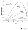
- Fig. 7 is a graph showing the angle dependency of the absorption coefficient of the microwave MW.
- the axis of abscissa represents the cosine of a radiation angle ⁇ of the microwave MW with respect to the radiation surface, and the axis of ordinate represents an absorption coefficient ⁇ .
- Fig. 7 shows that the absorption coefficient becomes the maximum when the radiation angle is almost 30° to 50°, although it may depend on an electron density n e of the plasma.
- the microwave MW is radiated at this angle ⁇ , plasma generation by the electric field of the microwave MW that has entered directly from the radial antenna 30A becomes dominant, so that the plasma distribution can be controlled accurately.
- the distribution in the space in the radial antenna 30A (that is, the gap between the two conductive plates 31A and 32 shown in Fig. 4(b)) is related to the distribution of the characteristic impedance of the radial antenna 30A.
- the distribution of the characteristic impedance is related to the distribution of the leakage amount of the microwave MW from the radial antenna 30A. More specifically, at the center of the radial antenna 30A (near the vertex of the circular conical surface) where the gap between the conductive plates 31A and 32 is small, the characteristic impedance is small, and accordingly the leakage amount is large.
- the characteristic impedance is large, and accordingly the leakage amount is small.
- the distribution of the leakage amount of the microwave MW may be adjusted, so that the distribution of plasma generation may be adjusted.
- the standing wave forming space S2 deforms. This changes the standing wave mode, so that the distribution of plasma generation may be changed.
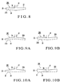
- Fig. 8 is a view schematically showing the sectional shape of a radial antenna according to the first modification.
- a conductive plate 31B having a downward convex circular conical surface may be used as the first conductive plate constituting the radiation surface.
- Fig. 9 includes views each schematically showing the sectional shape of a radial antenna according to the second modification.
- a radial antenna 30C shown in Fig. 9(a) is formed by arranging parallel to each other first and second conductive plates 31A and 32A forming upward convex circular conical surfaces.
- a radial antenna 30D shown in Fig. 9(b) is formed by arranging parallel to each other first and second conductive plates 31B and 32B forming downward convex circular conical surfaces.
- the distribution of plasma generation in the processing vessel 11 cannot be adjusted by adjusting the impedance distribution of the internal space.
- the plasma generating efficiency by the electric field of the microwave MW that has entered directly from the radial antenna 30C or 30D to the plasma can be improved, and the electric field of the standing wave can be weakened by deformation of the standing wave forming space S2. Therefore, a plasma distribution better than a conventional one can be obtained.
- Fig. 10 includes views each schematically showing the sectional shape of a radial antenna according to the third modification.
- a radial antenna 30E shown in Fig. 10(a) uses a flat plate-like conductive plate 31 as the first conductive plate constituting the radiation surface, and a conductive plate 32A forming an upward convex circular conical surface as the second conductive plate.
- a radial antenna 30F shown in Fig. 10(b) uses a flat plate-like conductive plate 31 as the first conductive plate similarly, and a conductive plate 32B forming a downward convex circular conical surface as the second conductive plate.
- the distribution of plasma generation in the processing vessel 11 can be adjusted by adjusting the impedance distribution of the internal space. Therefore, a plasma distribution better than the conventional one can be obtained.
- Each of the radial antennas 30A to 30F exemplified above uses a conductive plate forming an upward or downward convex circular conical surface as the first or second conductive plate.
- the first or second conductive plate may form another convex shape such as a curved surface.
- the radial antenna need not be of a leak type but can be of a so-called radiation type.
- the pitch among the slots 34 which are adjacent in the radial direction may be set to be almost equal to the wavelength ⁇ g of the microwave MW in the radial waveguide.
- Fig. 11 shows the arrangement of an etching apparatus according to the second embodiment of the present invention.
- the same portions as in Fig. 1 are denoted by the same reference numerals, and a description thereof will be omitted when necessary.
- a first conductive plate 31 constituting the radiation surface and a second waveguide 32 which forms a radial waveguide together with the conductive plate 31 are formed of parallel plates.
- the conductive plates 31 and 32 are arranged horizontally.
- a dielectric plate (first dielectric member) 13A opposed to the radiation surface of the radial antenna 30 forms a dome.
- the dielectric plate 13A has a surface inclining with respect to the radiation surface of the radial antenna 30.
- the dielectric plate 13A has a shape which is symmetrical with respect to the central axis.
- a cylindrical spacer 18 is interposed between the dielectric plate 13A and radial antenna 30.
- the dielectric plate 13, radial antenna 30A, and spacer 18 are covered by a shield material 17.
- the conductive plate 31 constituting the radiation surface of the radial antenna 30 is a horizontally arranged flat plate. Hence, a microwave MW leaking from slots 34 formed in the conductive plate 31 is radiated in the vertical direction (Z-axis direction).
- the plasma plane opposing the dielectric plate 13A forms a curved surface extending along the dielectric plate 13A.
- the direction of normal to the plasma plane inclines with respect to the vertical direction (Z-axis direction) except for its center.
- the microwave MW radiated from the conductive plate 31A in the vertical direction (Z-axis direction) enters the plasma in a direction inclining with respect to the direction of normal to the plasma plane opposing the dielectric plate 13A.
- This state is identical with the case which uses the radial antenna 30A shown in Fig. 1.
- plasma generation by the electric field of the microwave MW that has entered the plasma directly from the radial antenna 30 can be set dominant over plasma generation by the electric field of the standing wave.
- a plasma distribution better than the conventional one can be obtained.
- the dielectric plate 13A may have another convex shape such as an upward or downward convex circular conical surface.
- Fig. 12 shows the arrangement of an etching apparatus according to the third embodiment of the present invention to which a cavity antenna is applied.
- Fig. 12 the same portions as in Fig. 1 are denoted by the same reference numerals, and a description thereof will be omitted when necessary.
- Fig. 13 is a plan view of the radiation surface of the cavity antenna.
- a cavity antenna 70A is formed of a first conductive plate 71A constituting the radiation surface, a second conductive plate 72 arranged above the conductive plate 71A to oppose it, and a ring member 73 for closing the edges of the conductive plates 71A and 72.
- the conductive plates 71A and 72, and the ring member 73 are made of a conductor such as copper or aluminum.
- the conductive plate 72 which forms the antenna upper surface has a microwave inlet port 75 for introducing a microwave MW from a microwave generator 45 into the antenna.
- the microwave inlet port 75 need not be formed at the center of the conductive plate 72.
- the conductive plate 71A which forms the antenna lower surface has a plurality of concentric slots 74 extending in the circumferential direction, as shown in Fig. 13.
- the conductive plate 71A forms an upward convex circular conical surface in the same manner as the conductive plate 31A of the radial antenna 30A shown in Fig. 2. Accordingly, the circular conical surface of the conductive plate 71A inclines with respect to a flat plate-like dielectric plate 13.
- the conductive plates 71A and 72, and the ring member 73 form a cavity resonator which causes the microwave MW to resonate with a predetermined mode.
- a delay member may be arranged in the cavity resonator.
- each slot 74 formed in the conductive plate 71A, and a pitch P among the slots 74 which are adjacent in the radial direction are set on the basis of a wavelength ⁇ g of the microwave MW in the cavity resonator.
- the pitch P is desirably ⁇ g, but can be less than ⁇ g.
- reference numeral 48 denotes a cylindrical waveguide; and 49, a rectangular cylindrical converter.
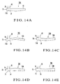
- Fig. 14 includes views each schematically showing the sectional shape of a modification of such a cavity antenna.
- a cavity antenna 70B shown in Fig. 14(a) uses a conductive plate 71B forming a downward convex circular conical surface as the first conductive plate constituting the radiation surface, and corresponds to the radial antenna 30B shown in Fig. 8.
- a cavity antenna 70C shown in Fig. 14(b) is formed by arranging parallel to each other first and second conductive plates 71A and 72A forming upward convex circular conical surfaces, and corresponds to the radial antenna 30C shown in Fig. 9(a).
- a cavity antenna 70D shown in Fig. 14(c) is formed by arranging parallel to each other first and second conductive plates 71B and 72B forming downward convex circular conical surfaces, and corresponds to the radial antenna 30D shown in Fig. 9(b).
- a cavity antenna 70E shown in Fig. 14(d) uses a flat plate-like conductive plate 71 as the first conductive plate and a conductive plate 72A forming an upward convex circular conical surface as the second conductive plate, and corresponds to the radial antenna 30E shown in Fig. 10(a).
- a cavity antenna 70F shown in Fig. 14(e) similarly uses a flat plate-like conductive plate 71 and a conductive plate 72B forming a downward convex circular conical surface as the second conductive plate, and corresponds to the radial antenna 30E shown in Fig. 10(b).
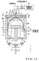
- Fig. 15 is a view showing the arrangement of an etching apparatus according to the fourth embodiment of the present invention.
- the same portions as in Fig. 1 are denoted by the same reference numerals, and a description thereof will be omitted when necessary.
- This etching apparatus has, in place of the dome-like dielectric plate 13A, a semispherical or bowl-like bell jar (first dielectric member) 83A which covers a substrate 21 located at a processing position. More specifically, the semispherical or bowl-like bell jar 83A is placed on the processing position from above with its opening facing down, and the edge of the opening of the bell jar 83A is fixed to the side wall of a processing vessel 11A below the processing position. Therefore, the side wall of the processing vessel 11A close to a space where a plasma is present with a comparatively high density is isolated from a susceptor 22A by the bell jar 83A.
- the bell jar 83A is made of a dielectric such as silica glass or ceramic material (e.g., Al 2 O 3 or AlN) with a thickness of about 3 mm to 30 mm.
- a seal member 12A such as an O-ring is interposed at the bonding portion between the processing vessel 11A and bell jar 83A.
- the susceptor 22A on which the substrate 21 is to be placed is supported by an elevating shaft 27 loosely extending through the bottom of the processing vessel 11A, so that it can move vertically.
- the susceptor 22A is moved downward.
- the susceptor 22A is moved upward so the substrate 21 can be located at the processing position.
- An insulating plate 24A made of a ceramic material or the like is formed on the bottom of the processing vessel 11A.
- a bellows 28 is provided between the susceptor 22A and insulating plate 24A to surround the elevating shaft 27.
- Exhaust ports 14A connected to a vacuum pump (not shown) are formed in the bottom of the processing vessel 11A, and a nozzle 15A for introducing a process gas and etching gas into the processing vessel is formed in the side wall of the processing vessel 11A.
- the nozzle 15A extends above the processing position of the substrate 21, so that the gas is discharged into the space above the susceptor 22A.
- the bell jar 83A forms a semispherical or bowl-like shape, and accordingly has a surface inclining with respect to the radiation surface (conductive plate 31) of a radial antenna 30.
- a plasma distribution better than the conventional one can be obtained, in the same manner as in the case of the etching apparatus shown in Fig. 11.
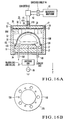
- Fig. 16 includes views showing a modification of the etching apparatus shown in Fig. 15, in which Fig. 16(a) is a sectional view, and Fig. 16(b) is a plan view of a susceptor 22.
- Fig. 16(a) is a sectional view
- Fig. 16(b) is a plan view of a susceptor 22.
- the same portions as in Fig. 11 are denoted by the same reference numerals, and a description thereof will be omitted when necessary.
- a semispherical or bowl-like bell jar (first dielectric member) 83B may be arranged on the upper surface of the susceptor 22.
- the susceptor 22 sealed by a seal material 12B and the bell jar 83B form the processing vessel.
- An exhaust through hole 14B and gas inlet through hole 15B are formed in each of the susceptor 22, a support table 23, an insulating plate 24, and the bottom of a processing vessel 11.
- the through holes 14B and 15B are formed in the peripheries of the susceptor 22 and the like.
- a guide 15C shown in Fig. 16(a) may be attached to the gas inlet through hole 15B, so the gas introduced from the through hole 15B will not be directly exhausted from the adjacent through hole 14B.
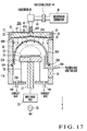
- Fig. 17 shows the arrangement of an etching apparatus according to the fifth embodiment of the present invention.
- the same portions as in Figs. 1 and 15 are denoted by the same reference numerals, and a description thereof will be omitted when necessary.
- This etching apparatus is formed by combining a radial antenna 30A having a circular conical radiation surface and a semispherical or bowl-like bell jar 83A.
- a change in radiation angle of a microwave MW depending on the antenna shape and a change in angle of the plasma plane depending on the bell jar shape act with each other, the planar distribution of the efficiency with which the microwave MW is absorbed by the plasma can be adjusted.
- the combination of the antenna and bell jar or dielectric plate is not limited to the described one, but any combination of any one of the radial antennas 30A to 30F and the bell jar 83A or 83B or dielectric plate 13A can be used.
- Fig. 19 shows the arrangement of a CVD apparatus according to the sixth embodiment of the present invention.
- the same portions as in Fig. 17 are denoted by the same reference numerals, and a description thereof will be omitted when necessary.
- This CVD apparatus has a heater 91 for heating a substrate 21, a gas supply nozzle 92 for introducing a gas mixture of SiH 4 and H 2 into the processing vessel, and the like, which are an arrangement necessary as an CVD apparatus, and also has a radial antenna 30A with a circular conical radiation surface, and a semispherical or bowl-like bell jar (first dielectric member) 83A for covering the substrate 21 located at the processing position.
- this CVD apparatus has the same characteristic features as those of the etching apparatus shown in Fig. 16.
- the upper opening of a processing vessel 11A is sealed by a dielectric plate (second dielectric member) 13.
- a nozzle 93 and exhaust port 94 are formed as communication means in the side wall of the processing vessel 11A, so that a gas at a predetermined temperature is supplied to the sealed space surrounded by the bell jar 83A, dielectric plate 13, and processing vessel 11A, thus adjusting the temperature of the bell jar 83A.
- the gas to be introduced from the nozzle 93 for example, N 2 is used as a gas that does not absorb a microwave MW easily.
- the temperature of this gas is set to a temperature higher than that of the bell jar 83A, and its upper limit is set to 600°C.
- the heater 91 is set to about 150°C to heat the substrate 21, and a gas mixture of SiH 4 and H 2 is introduced into the processing vessel from the gas supply nozzle 92.
- SiH x reacts with the surface of the substrate 21 to form an amorphous Si (to be abbreviated as a-Si hereinafter) film.
- a-Si amorphous Si
- This a-Si interferes with the microwave MW from being introduced from the radial antenna 30A.
- N 2 at a temperature of 600°C or less, e.g., 150°C to 300°C is supplied into the space between the bell jar 83A and dielectric plate 13 so as to heat the bell jar 83A, SiH x does not attach easily. Therefore, formation of the a-Si film on the inner surface of the bell jar 83A can be reduced. As a result, loss of the microwave MW introduced into the processing vessel through the bell jar 83A is reduced, and a plasma is generated efficiently to form a film.
- the fluid to be supplied into the sealed space surrounded by the bell jar 83A, dielectric plate 13, and processing vessel 11A need not be a gas but may be a liquid.
- a liquid that does not absorb the microwave MW easily e.g., galden (perfluoropolyether) or fluoricate, is preferably used.
- a fluid with a temperature lower than the above temperature may be supplied into the sealed space to cool the bell jar 83A. If the temperature of the bell jar 83A becomes excessively high due to the function of the microwave MW, the bell jar 83A may be broken. In the etching apparatus shown in Fig. 16, the resist on the substrate 21 may be sometimes burned by the radiation heat of the bell jar 83A, and a desired pattern cannot be etched. If the bell jar 83A is cooled in the above manner, this problem can be avoided.
- the second dielectric member which forms the sealed space together with the bell jar 83A may be arranged on a side different from a susceptor 22A with respect to the bell jar 83A. Hence, the second dielectric member may be filled midway along a coaxial cable 41 as the feeder of the radial antenna 30A, thus forming a sealed space. In this case, the fluid is supplied into the radial antenna 30A as well.
- a radial antenna is used as the slot antenna.
- the cavity antenna shown in Figs. 12 to 14 is used as well, the same effect can be obtained.
- At least one of the first and second conductive plates that form a slot antenna inclines relative to the first dielectric member opposed to the first dielectric plate are provided.
- the first conductive plate constituting the radiation surface inclines with respect to the first dielectric member plasma generation by the electric field of the electromagnetic field which enters directly from the slot antenna can be set dominant over plasma generation by the electric field of the standing wave formed in the processing vessel. Since the space between the first conductive plate and plasma plane deforms, the standing wave mode changes.
- the distribution of the characteristic impedance of the antenna is adjusted, so that the distribution of the radiation amount of the antenna is adjusted.
- the plasma processing apparatus according to the present invention can be applied to processing apparatuses such as an etching apparatus, CVD apparatus, and ashing apparatus.
Landscapes
- Chemical & Material Sciences (AREA)
- Engineering & Computer Science (AREA)
- Chemical Kinetics & Catalysis (AREA)
- Organic Chemistry (AREA)
- Metallurgy (AREA)
- General Chemical & Material Sciences (AREA)
- Materials Engineering (AREA)
- Mechanical Engineering (AREA)
- Physics & Mathematics (AREA)
- Plasma & Fusion (AREA)
- Analytical Chemistry (AREA)
- Inorganic Chemistry (AREA)
- Health & Medical Sciences (AREA)
- General Health & Medical Sciences (AREA)
- Toxicology (AREA)
- Plasma Technology (AREA)
- Drying Of Semiconductors (AREA)
- Physical Or Chemical Processes And Apparatus (AREA)
- Chemical Vapour Deposition (AREA)
Abstract
Description
Claims (11)
- A plasma processing apparatus comprising a processing vessel in which a susceptor for placing a target object thereon is arranged, a slot antenna opposed to said susceptor to supply an electromagnetic field into said processing vessel, and a first dielectric member opposed to a radiation surface of said slot antenna, characterized in that
said slot antenna comprisesa first conductive plate constituting the radiation surface, anda second conductive plate arranged on a side opposite to said susceptor when seen from said first conductive plate, andat least one of said first and second conductive plates inclines relative to said first dielectric member. - A plasma processing apparatus according to claim 1, characterized in that said slot antenna is a radial antenna.
- A plasma processing apparatus according to claim 1, characterized in that said slot antenna is a cavity antenna.
- A plasma processing apparatus according to claim 1, characterized in that said first and second conductive plates of said slot antenna, and said first dielectric member are symmetrical with respect to a common central axis.
- A plasma processing apparatus according to claim 1, characterized in that at least one of said first and second conductive plates of said slot antenna and said first dielectric member has an upward convex shape.
- A plasma processing apparatus according to claim 1, characterized in that at least one of said first and second conductive plates of said slot antenna and said first dielectric member has a downward convex shape.
- A plasma processing apparatus according to claim 1, characterized in that a gap between said first and second conductive plates is not less than 5 mm and less than λg/2 where λg (λg > 10 mm) is the wavelength of an electromagnetic field between said first and second conductive plates.
- A plasma processing apparatus according to claim 1, characterized in that said first dielectric member has a flat plate-like shape.
- A plasma processing apparatus according to claim 1, characterized in that said first dielectric member has a dome-like shape.
- A plasma processing apparatus according to claim 1, characterized in that said first dielectric member is a bell jar which isolates at least part of an inner surface of said processing vessel from said susceptor.
- A plasma processing apparatus according to claim 10, characterized by further comprisinga second dielectric member arranged on a side different from said susceptor with respect to said first dielectric member and serving to form a sealed space together with said first dielectric member, andsupply means for supplying a fluid in said sealed space so as to adjust a temperature of said first dielectric member.
Applications Claiming Priority (5)
| Application Number | Priority Date | Filing Date | Title |
|---|---|---|---|
| JP2000209590 | 2000-07-11 | ||
| JP2000209590 | 2000-07-11 | ||
| JP2001010780 | 2001-01-18 | ||
| JP2001010780A JP3485896B2 (en) | 2000-07-11 | 2001-01-18 | Plasma processing equipment |
| PCT/JP2001/006004 WO2002005339A1 (en) | 2000-07-11 | 2001-07-11 | Plasma processing apparatus |
Publications (3)
| Publication Number | Publication Date |
|---|---|
| EP1306893A1 true EP1306893A1 (en) | 2003-05-02 |
| EP1306893A4 EP1306893A4 (en) | 2005-09-28 |
| EP1306893B1 EP1306893B1 (en) | 2009-12-16 |
Family
ID=26595784
Family Applications (1)
| Application Number | Title | Priority Date | Filing Date |
|---|---|---|---|
| EP01949933A Expired - Lifetime EP1306893B1 (en) | 2000-07-11 | 2001-07-11 | Plasma processing apparatus |
Country Status (8)
| Country | Link |
|---|---|
| US (1) | US7395779B2 (en) |
| EP (1) | EP1306893B1 (en) |
| JP (1) | JP3485896B2 (en) |
| KR (1) | KR100507717B1 (en) |
| AU (1) | AU2001271030A1 (en) |
| DE (1) | DE60140809D1 (en) |
| TW (1) | TW502561B (en) |
| WO (1) | WO2002005339A1 (en) |
Cited By (2)
| Publication number | Priority date | Publication date | Assignee | Title |
|---|---|---|---|---|
| DE102006006289A1 (en) * | 2006-02-10 | 2007-08-23 | R3T Gmbh Rapid Reactive Radicals Technology | Apparatus and method for producing excited and / or ionized particles in a plasma |
| WO2020020014A1 (en) * | 2018-07-27 | 2020-01-30 | 北京北方华创微电子装备有限公司 | Surface wave plasma device |
Families Citing this family (330)
| Publication number | Priority date | Publication date | Assignee | Title |
|---|---|---|---|---|
| US20040173314A1 (en) * | 2003-03-05 | 2004-09-09 | Ryoji Nishio | Plasma processing apparatus and method |
| DE10317027A1 (en) * | 2003-04-11 | 2004-11-11 | Leybold Optics Gmbh | High frequency plasma beam source and method for irradiating a surface |
| JP3974553B2 (en) * | 2003-05-07 | 2007-09-12 | 東京エレクトロン株式会社 | Plasma processing apparatus, antenna for plasma processing apparatus, and plasma processing method |
| US7396431B2 (en) * | 2004-09-30 | 2008-07-08 | Tokyo Electron Limited | Plasma processing system for treating a substrate |
| US7584714B2 (en) * | 2004-09-30 | 2009-09-08 | Tokyo Electron Limited | Method and system for improving coupling between a surface wave plasma source and a plasma space |
| JP4953153B2 (en) * | 2005-07-28 | 2012-06-13 | 住友電気工業株式会社 | Microwave plasma CVD equipment |
| US7493869B1 (en) | 2005-12-16 | 2009-02-24 | The United States Of America As Represented By The Administration Of Nasa | Very large area/volume microwave ECR plasma and ion source |
| US7938081B2 (en) * | 2006-09-12 | 2011-05-10 | Tokyo Electron Limited | Radial line slot antenna having a conductive layer |
| EP2108714B1 (en) * | 2007-01-29 | 2014-03-12 | Sumitomo Electric Industries, Ltd. | Microwave plasma cvd system |
| KR100860473B1 (en) * | 2007-04-18 | 2008-09-26 | 에스엔유 프리시젼 주식회사 | Plasma Monitoring Device |
| US20080303744A1 (en) * | 2007-06-11 | 2008-12-11 | Tokyo Electron Limited | Plasma processing system, antenna, and use of plasma processing system |
| US8753475B2 (en) * | 2008-02-08 | 2014-06-17 | Tokyo Electron Limited | Plasma processing apparatus |
| US9394608B2 (en) | 2009-04-06 | 2016-07-19 | Asm America, Inc. | Semiconductor processing reactor and components thereof |
| US8540818B2 (en) * | 2009-04-28 | 2013-09-24 | Mitsubishi Materials Corporation | Polycrystalline silicon reactor |
| US8802201B2 (en) | 2009-08-14 | 2014-08-12 | Asm America, Inc. | Systems and methods for thin-film deposition of metal oxides using excited nitrogen-oxygen species |
| JP5479013B2 (en) * | 2009-09-30 | 2014-04-23 | 東京エレクトロン株式会社 | Plasma processing apparatus and slow wave plate used therefor |
| WO2012051198A1 (en) | 2010-10-12 | 2012-04-19 | Goji Ltd. | Device and method for applying electromagnetic energy to a container |
| US20130023129A1 (en) | 2011-07-20 | 2013-01-24 | Asm America, Inc. | Pressure transmitter for a semiconductor processing environment |
| US9017481B1 (en) | 2011-10-28 | 2015-04-28 | Asm America, Inc. | Process feed management for semiconductor substrate processing |
| US9048070B2 (en) * | 2011-11-11 | 2015-06-02 | Tokyo Electron Limited | Dielectric window for plasma treatment device, and plasma treatment device |
| US10714315B2 (en) | 2012-10-12 | 2020-07-14 | Asm Ip Holdings B.V. | Semiconductor reaction chamber showerhead |
| US20160376700A1 (en) | 2013-02-01 | 2016-12-29 | Asm Ip Holding B.V. | System for treatment of deposition reactor |
| JP5728565B2 (en) * | 2013-12-24 | 2015-06-03 | 東京エレクトロン株式会社 | Plasma processing apparatus and slow wave plate used therefor |
| JP5805227B2 (en) * | 2014-01-28 | 2015-11-04 | 東京エレクトロン株式会社 | Plasma processing equipment |
| US11015245B2 (en) | 2014-03-19 | 2021-05-25 | Asm Ip Holding B.V. | Gas-phase reactor and system having exhaust plenum and components thereof |
| US10858737B2 (en) | 2014-07-28 | 2020-12-08 | Asm Ip Holding B.V. | Showerhead assembly and components thereof |
| JP2016039356A (en) * | 2014-08-06 | 2016-03-22 | ピーエスケー・インコーポレーテッド | Baffle and substrate treating apparatus including the same |
| US9890456B2 (en) | 2014-08-21 | 2018-02-13 | Asm Ip Holding B.V. | Method and system for in situ formation of gas-phase compounds |
| US10941490B2 (en) | 2014-10-07 | 2021-03-09 | Asm Ip Holding B.V. | Multiple temperature range susceptor, assembly, reactor and system including the susceptor, and methods of using the same |
| US10276355B2 (en) | 2015-03-12 | 2019-04-30 | Asm Ip Holding B.V. | Multi-zone reactor, system including the reactor, and method of using the same |
| US10458018B2 (en) | 2015-06-26 | 2019-10-29 | Asm Ip Holding B.V. | Structures including metal carbide material, devices including the structures, and methods of forming same |
| US10211308B2 (en) | 2015-10-21 | 2019-02-19 | Asm Ip Holding B.V. | NbMC layers |
| US11139308B2 (en) | 2015-12-29 | 2021-10-05 | Asm Ip Holding B.V. | Atomic layer deposition of III-V compounds to form V-NAND devices |
| US10529554B2 (en) | 2016-02-19 | 2020-01-07 | Asm Ip Holding B.V. | Method for forming silicon nitride film selectively on sidewalls or flat surfaces of trenches |
| US10343920B2 (en) | 2016-03-18 | 2019-07-09 | Asm Ip Holding B.V. | Aligned carbon nanotubes |
| US10190213B2 (en) | 2016-04-21 | 2019-01-29 | Asm Ip Holding B.V. | Deposition of metal borides |
| US10865475B2 (en) | 2016-04-21 | 2020-12-15 | Asm Ip Holding B.V. | Deposition of metal borides and silicides |
| US10367080B2 (en) | 2016-05-02 | 2019-07-30 | Asm Ip Holding B.V. | Method of forming a germanium oxynitride film |
| US11453943B2 (en) | 2016-05-25 | 2022-09-27 | Asm Ip Holding B.V. | Method for forming carbon-containing silicon/metal oxide or nitride film by ALD using silicon precursor and hydrocarbon precursor |
| US9859151B1 (en) | 2016-07-08 | 2018-01-02 | Asm Ip Holding B.V. | Selective film deposition method to form air gaps |
| US10612137B2 (en) | 2016-07-08 | 2020-04-07 | Asm Ip Holdings B.V. | Organic reactants for atomic layer deposition |
| US9812320B1 (en) | 2016-07-28 | 2017-11-07 | Asm Ip Holding B.V. | Method and apparatus for filling a gap |
| US9887082B1 (en) | 2016-07-28 | 2018-02-06 | Asm Ip Holding B.V. | Method and apparatus for filling a gap |
| KR102532607B1 (en) | 2016-07-28 | 2023-05-15 | 에이에스엠 아이피 홀딩 비.브이. | Substrate processing apparatus and method of operating the same |
| US10643826B2 (en) | 2016-10-26 | 2020-05-05 | Asm Ip Holdings B.V. | Methods for thermally calibrating reaction chambers |
| US11532757B2 (en) | 2016-10-27 | 2022-12-20 | Asm Ip Holding B.V. | Deposition of charge trapping layers |
| US10229833B2 (en) | 2016-11-01 | 2019-03-12 | Asm Ip Holding B.V. | Methods for forming a transition metal nitride film on a substrate by atomic layer deposition and related semiconductor device structures |
| US10714350B2 (en) | 2016-11-01 | 2020-07-14 | ASM IP Holdings, B.V. | Methods for forming a transition metal niobium nitride film on a substrate by atomic layer deposition and related semiconductor device structures |
| KR102546317B1 (en) | 2016-11-15 | 2023-06-21 | 에이에스엠 아이피 홀딩 비.브이. | Gas supply unit and substrate processing apparatus including the same |
| KR102762543B1 (en) * | 2016-12-14 | 2025-02-05 | 에이에스엠 아이피 홀딩 비.브이. | Substrate processing apparatus |
| US11581186B2 (en) | 2016-12-15 | 2023-02-14 | Asm Ip Holding B.V. | Sequential infiltration synthesis apparatus |
| US11447861B2 (en) | 2016-12-15 | 2022-09-20 | Asm Ip Holding B.V. | Sequential infiltration synthesis apparatus and a method of forming a patterned structure |
| KR102700194B1 (en) | 2016-12-19 | 2024-08-28 | 에이에스엠 아이피 홀딩 비.브이. | Substrate processing apparatus |
| US10269558B2 (en) | 2016-12-22 | 2019-04-23 | Asm Ip Holding B.V. | Method of forming a structure on a substrate |
| US10867788B2 (en) | 2016-12-28 | 2020-12-15 | Asm Ip Holding B.V. | Method of forming a structure on a substrate |
| US11390950B2 (en) | 2017-01-10 | 2022-07-19 | Asm Ip Holding B.V. | Reactor system and method to reduce residue buildup during a film deposition process |
| US10468261B2 (en) | 2017-02-15 | 2019-11-05 | Asm Ip Holding B.V. | Methods for forming a metallic film on a substrate by cyclical deposition and related semiconductor device structures |
| US10529563B2 (en) | 2017-03-29 | 2020-01-07 | Asm Ip Holdings B.V. | Method for forming doped metal oxide films on a substrate by cyclical deposition and related semiconductor device structures |
| KR102457289B1 (en) | 2017-04-25 | 2022-10-21 | 에이에스엠 아이피 홀딩 비.브이. | Method for depositing a thin film and manufacturing a semiconductor device |
| US10892156B2 (en) | 2017-05-08 | 2021-01-12 | Asm Ip Holding B.V. | Methods for forming a silicon nitride film on a substrate and related semiconductor device structures |
| US10770286B2 (en) | 2017-05-08 | 2020-09-08 | Asm Ip Holdings B.V. | Methods for selectively forming a silicon nitride film on a substrate and related semiconductor device structures |
| US10886123B2 (en) | 2017-06-02 | 2021-01-05 | Asm Ip Holding B.V. | Methods for forming low temperature semiconductor layers and related semiconductor device structures |
| US12040200B2 (en) | 2017-06-20 | 2024-07-16 | Asm Ip Holding B.V. | Semiconductor processing apparatus and methods for calibrating a semiconductor processing apparatus |
| US11306395B2 (en) | 2017-06-28 | 2022-04-19 | Asm Ip Holding B.V. | Methods for depositing a transition metal nitride film on a substrate by atomic layer deposition and related deposition apparatus |
| KR20190009245A (en) | 2017-07-18 | 2019-01-28 | 에이에스엠 아이피 홀딩 비.브이. | Methods for forming a semiconductor device structure and related semiconductor device structures |
| US11374112B2 (en) | 2017-07-19 | 2022-06-28 | Asm Ip Holding B.V. | Method for depositing a group IV semiconductor and related semiconductor device structures |
| US11018002B2 (en) | 2017-07-19 | 2021-05-25 | Asm Ip Holding B.V. | Method for selectively depositing a Group IV semiconductor and related semiconductor device structures |
| US10541333B2 (en) | 2017-07-19 | 2020-01-21 | Asm Ip Holding B.V. | Method for depositing a group IV semiconductor and related semiconductor device structures |
| US10590535B2 (en) | 2017-07-26 | 2020-03-17 | Asm Ip Holdings B.V. | Chemical treatment, deposition and/or infiltration apparatus and method for using the same |
| TWI815813B (en) | 2017-08-04 | 2023-09-21 | 荷蘭商Asm智慧財產控股公司 | Showerhead assembly for distributing a gas within a reaction chamber |
| US10770336B2 (en) | 2017-08-08 | 2020-09-08 | Asm Ip Holding B.V. | Substrate lift mechanism and reactor including same |
| US10692741B2 (en) | 2017-08-08 | 2020-06-23 | Asm Ip Holdings B.V. | Radiation shield |
| US11139191B2 (en) | 2017-08-09 | 2021-10-05 | Asm Ip Holding B.V. | Storage apparatus for storing cassettes for substrates and processing apparatus equipped therewith |
| US11769682B2 (en) | 2017-08-09 | 2023-09-26 | Asm Ip Holding B.V. | Storage apparatus for storing cassettes for substrates and processing apparatus equipped therewith |
| US11830730B2 (en) | 2017-08-29 | 2023-11-28 | Asm Ip Holding B.V. | Layer forming method and apparatus |
| US11295980B2 (en) | 2017-08-30 | 2022-04-05 | Asm Ip Holding B.V. | Methods for depositing a molybdenum metal film over a dielectric surface of a substrate by a cyclical deposition process and related semiconductor device structures |
| US11056344B2 (en) | 2017-08-30 | 2021-07-06 | Asm Ip Holding B.V. | Layer forming method |
| KR102491945B1 (en) | 2017-08-30 | 2023-01-26 | 에이에스엠 아이피 홀딩 비.브이. | Substrate processing apparatus |
| KR102401446B1 (en) | 2017-08-31 | 2022-05-24 | 에이에스엠 아이피 홀딩 비.브이. | Substrate processing apparatus |
| KR102630301B1 (en) | 2017-09-21 | 2024-01-29 | 에이에스엠 아이피 홀딩 비.브이. | Method of sequential infiltration synthesis treatment of infiltrateable material and structures and devices formed using same |
| US10844484B2 (en) | 2017-09-22 | 2020-11-24 | Asm Ip Holding B.V. | Apparatus for dispensing a vapor phase reactant to a reaction chamber and related methods |
| US10658205B2 (en) | 2017-09-28 | 2020-05-19 | Asm Ip Holdings B.V. | Chemical dispensing apparatus and methods for dispensing a chemical to a reaction chamber |
| US10403504B2 (en) | 2017-10-05 | 2019-09-03 | Asm Ip Holding B.V. | Method for selectively depositing a metallic film on a substrate |
| US10923344B2 (en) | 2017-10-30 | 2021-02-16 | Asm Ip Holding B.V. | Methods for forming a semiconductor structure and related semiconductor structures |
| US10910262B2 (en) | 2017-11-16 | 2021-02-02 | Asm Ip Holding B.V. | Method of selectively depositing a capping layer structure on a semiconductor device structure |
| US11022879B2 (en) | 2017-11-24 | 2021-06-01 | Asm Ip Holding B.V. | Method of forming an enhanced unexposed photoresist layer |
| TWI791689B (en) | 2017-11-27 | 2023-02-11 | 荷蘭商Asm智慧財產控股私人有限公司 | Apparatus including a clean mini environment |
| JP7214724B2 (en) | 2017-11-27 | 2023-01-30 | エーエスエム アイピー ホールディング ビー.ブイ. | Storage device for storing wafer cassettes used in batch furnaces |
| US10872771B2 (en) | 2018-01-16 | 2020-12-22 | Asm Ip Holding B. V. | Method for depositing a material film on a substrate within a reaction chamber by a cyclical deposition process and related device structures |
| KR102695659B1 (en) | 2018-01-19 | 2024-08-14 | 에이에스엠 아이피 홀딩 비.브이. | Method for depositing a gap filling layer by plasma assisted deposition |
| TWI799494B (en) | 2018-01-19 | 2023-04-21 | 荷蘭商Asm 智慧財產控股公司 | Deposition method |
| US11018047B2 (en) | 2018-01-25 | 2021-05-25 | Asm Ip Holding B.V. | Hybrid lift pin |
| USD880437S1 (en) | 2018-02-01 | 2020-04-07 | Asm Ip Holding B.V. | Gas supply plate for semiconductor manufacturing apparatus |
| US11081345B2 (en) | 2018-02-06 | 2021-08-03 | Asm Ip Holding B.V. | Method of post-deposition treatment for silicon oxide film |
| US11685991B2 (en) | 2018-02-14 | 2023-06-27 | Asm Ip Holding B.V. | Method for depositing a ruthenium-containing film on a substrate by a cyclical deposition process |
| US10896820B2 (en) | 2018-02-14 | 2021-01-19 | Asm Ip Holding B.V. | Method for depositing a ruthenium-containing film on a substrate by a cyclical deposition process |
| US10731249B2 (en) | 2018-02-15 | 2020-08-04 | Asm Ip Holding B.V. | Method of forming a transition metal containing film on a substrate by a cyclical deposition process, a method for supplying a transition metal halide compound to a reaction chamber, and related vapor deposition apparatus |
| KR102636427B1 (en) | 2018-02-20 | 2024-02-13 | 에이에스엠 아이피 홀딩 비.브이. | Substrate processing method and apparatus |
| US10975470B2 (en) | 2018-02-23 | 2021-04-13 | Asm Ip Holding B.V. | Apparatus for detecting or monitoring for a chemical precursor in a high temperature environment |
| US11473195B2 (en) | 2018-03-01 | 2022-10-18 | Asm Ip Holding B.V. | Semiconductor processing apparatus and a method for processing a substrate |
| US11629406B2 (en) | 2018-03-09 | 2023-04-18 | Asm Ip Holding B.V. | Semiconductor processing apparatus comprising one or more pyrometers for measuring a temperature of a substrate during transfer of the substrate |
| US11114283B2 (en) | 2018-03-16 | 2021-09-07 | Asm Ip Holding B.V. | Reactor, system including the reactor, and methods of manufacturing and using same |
| KR102646467B1 (en) | 2018-03-27 | 2024-03-11 | 에이에스엠 아이피 홀딩 비.브이. | Method of forming an electrode on a substrate and a semiconductor device structure including an electrode |
| US11230766B2 (en) | 2018-03-29 | 2022-01-25 | Asm Ip Holding B.V. | Substrate processing apparatus and method |
| US11088002B2 (en) | 2018-03-29 | 2021-08-10 | Asm Ip Holding B.V. | Substrate rack and a substrate processing system and method |
| KR102501472B1 (en) | 2018-03-30 | 2023-02-20 | 에이에스엠 아이피 홀딩 비.브이. | Substrate processing method |
| KR102600229B1 (en) | 2018-04-09 | 2023-11-10 | 에이에스엠 아이피 홀딩 비.브이. | Substrate supporting device, substrate processing apparatus including the same and substrate processing method |
| US12025484B2 (en) | 2018-05-08 | 2024-07-02 | Asm Ip Holding B.V. | Thin film forming method |
| TWI843623B (en) | 2018-05-08 | 2024-05-21 | 荷蘭商Asm Ip私人控股有限公司 | Methods for depositing an oxide film on a substrate by a cyclical deposition process and related device structures |
| US12272527B2 (en) | 2018-05-09 | 2025-04-08 | Asm Ip Holding B.V. | Apparatus for use with hydrogen radicals and method of using same |
| KR20190129718A (en) | 2018-05-11 | 2019-11-20 | 에이에스엠 아이피 홀딩 비.브이. | Methods for forming a doped metal carbide film on a substrate and related semiconductor device structures |
| KR102596988B1 (en) | 2018-05-28 | 2023-10-31 | 에이에스엠 아이피 홀딩 비.브이. | Method of processing a substrate and a device manufactured by the same |
| US11718913B2 (en) | 2018-06-04 | 2023-08-08 | Asm Ip Holding B.V. | Gas distribution system and reactor system including same |
| TWI840362B (en) | 2018-06-04 | 2024-05-01 | 荷蘭商Asm Ip私人控股有限公司 | Wafer handling chamber with moisture reduction |
| US11286562B2 (en) | 2018-06-08 | 2022-03-29 | Asm Ip Holding B.V. | Gas-phase chemical reactor and method of using same |
| KR102568797B1 (en) | 2018-06-21 | 2023-08-21 | 에이에스엠 아이피 홀딩 비.브이. | Substrate processing system |
| US10797133B2 (en) | 2018-06-21 | 2020-10-06 | Asm Ip Holding B.V. | Method for depositing a phosphorus doped silicon arsenide film and related semiconductor device structures |
| US11499222B2 (en) | 2018-06-27 | 2022-11-15 | Asm Ip Holding B.V. | Cyclic deposition methods for forming metal-containing material and films and structures including the metal-containing material |
| TWI871083B (en) | 2018-06-27 | 2025-01-21 | 荷蘭商Asm Ip私人控股有限公司 | Cyclic deposition processes for forming metal-containing material |
| KR102686758B1 (en) | 2018-06-29 | 2024-07-18 | 에이에스엠 아이피 홀딩 비.브이. | Method for depositing a thin film and manufacturing a semiconductor device |
| US10612136B2 (en) | 2018-06-29 | 2020-04-07 | ASM IP Holding, B.V. | Temperature-controlled flange and reactor system including same |
| US10388513B1 (en) | 2018-07-03 | 2019-08-20 | Asm Ip Holding B.V. | Method for depositing silicon-free carbon-containing film as gap-fill layer by pulse plasma-assisted deposition |
| US10755922B2 (en) | 2018-07-03 | 2020-08-25 | Asm Ip Holding B.V. | Method for depositing silicon-free carbon-containing film as gap-fill layer by pulse plasma-assisted deposition |
| US10767789B2 (en) | 2018-07-16 | 2020-09-08 | Asm Ip Holding B.V. | Diaphragm valves, valve components, and methods for forming valve components |
| US11053591B2 (en) | 2018-08-06 | 2021-07-06 | Asm Ip Holding B.V. | Multi-port gas injection system and reactor system including same |
| US10883175B2 (en) | 2018-08-09 | 2021-01-05 | Asm Ip Holding B.V. | Vertical furnace for processing substrates and a liner for use therein |
| US10829852B2 (en) | 2018-08-16 | 2020-11-10 | Asm Ip Holding B.V. | Gas distribution device for a wafer processing apparatus |
| US11430674B2 (en) | 2018-08-22 | 2022-08-30 | Asm Ip Holding B.V. | Sensor array, apparatus for dispensing a vapor phase reactant to a reaction chamber and related methods |
| US11024523B2 (en) | 2018-09-11 | 2021-06-01 | Asm Ip Holding B.V. | Substrate processing apparatus and method |
| KR102707956B1 (en) | 2018-09-11 | 2024-09-19 | 에이에스엠 아이피 홀딩 비.브이. | Method for deposition of a thin film |
| US11049751B2 (en) | 2018-09-14 | 2021-06-29 | Asm Ip Holding B.V. | Cassette supply system to store and handle cassettes and processing apparatus equipped therewith |
| US10818482B2 (en) * | 2018-09-27 | 2020-10-27 | Tokyo Electron Limited | Methods for stability monitoring and improvements to plasma sources for plasma processing |
| CN110970344B (en) | 2018-10-01 | 2024-10-25 | Asmip控股有限公司 | Substrate holding device, system including the same and method of using the same |
| US11232963B2 (en) | 2018-10-03 | 2022-01-25 | Asm Ip Holding B.V. | Substrate processing apparatus and method |
| KR102592699B1 (en) | 2018-10-08 | 2023-10-23 | 에이에스엠 아이피 홀딩 비.브이. | Substrate support unit and apparatuses for depositing thin film and processing the substrate including the same |
| KR102546322B1 (en) | 2018-10-19 | 2023-06-21 | 에이에스엠 아이피 홀딩 비.브이. | Substrate processing apparatus and substrate processing method |
| KR102605121B1 (en) | 2018-10-19 | 2023-11-23 | 에이에스엠 아이피 홀딩 비.브이. | Substrate processing apparatus and substrate processing method |
| USD948463S1 (en) | 2018-10-24 | 2022-04-12 | Asm Ip Holding B.V. | Susceptor for semiconductor substrate supporting apparatus |
| US12378665B2 (en) | 2018-10-26 | 2025-08-05 | Asm Ip Holding B.V. | High temperature coatings for a preclean and etch apparatus and related methods |
| US11087997B2 (en) | 2018-10-31 | 2021-08-10 | Asm Ip Holding B.V. | Substrate processing apparatus for processing substrates |
| KR102748291B1 (en) | 2018-11-02 | 2024-12-31 | 에이에스엠 아이피 홀딩 비.브이. | Substrate support unit and substrate processing apparatus including the same |
| US11572620B2 (en) | 2018-11-06 | 2023-02-07 | Asm Ip Holding B.V. | Methods for selectively depositing an amorphous silicon film on a substrate |
| US11031242B2 (en) | 2018-11-07 | 2021-06-08 | Asm Ip Holding B.V. | Methods for depositing a boron doped silicon germanium film |
| US10818758B2 (en) | 2018-11-16 | 2020-10-27 | Asm Ip Holding B.V. | Methods for forming a metal silicate film on a substrate in a reaction chamber and related semiconductor device structures |
| US10847366B2 (en) | 2018-11-16 | 2020-11-24 | Asm Ip Holding B.V. | Methods for depositing a transition metal chalcogenide film on a substrate by a cyclical deposition process |
| US12040199B2 (en) | 2018-11-28 | 2024-07-16 | Asm Ip Holding B.V. | Substrate processing apparatus for processing substrates |
| US11217444B2 (en) | 2018-11-30 | 2022-01-04 | Asm Ip Holding B.V. | Method for forming an ultraviolet radiation responsive metal oxide-containing film |
| KR102636428B1 (en) | 2018-12-04 | 2024-02-13 | 에이에스엠 아이피 홀딩 비.브이. | A method for cleaning a substrate processing apparatus |
| US11158513B2 (en) | 2018-12-13 | 2021-10-26 | Asm Ip Holding B.V. | Methods for forming a rhenium-containing film on a substrate by a cyclical deposition process and related semiconductor device structures |
| JP7504584B2 (en) | 2018-12-14 | 2024-06-24 | エーエスエム・アイピー・ホールディング・ベー・フェー | Method and system for forming device structures using selective deposition of gallium nitride - Patents.com |
| TWI866480B (en) | 2019-01-17 | 2024-12-11 | 荷蘭商Asm Ip 私人控股有限公司 | Methods of forming a transition metal containing film on a substrate by a cyclical deposition process |
| KR102727227B1 (en) | 2019-01-22 | 2024-11-07 | 에이에스엠 아이피 홀딩 비.브이. | Semiconductor processing device |
| CN111524788B (en) | 2019-02-01 | 2023-11-24 | Asm Ip私人控股有限公司 | Method for forming topologically selective films of silicon oxide |
| KR102626263B1 (en) | 2019-02-20 | 2024-01-16 | 에이에스엠 아이피 홀딩 비.브이. | Cyclical deposition method including treatment step and apparatus for same |
| TWI873122B (en) | 2019-02-20 | 2025-02-21 | 荷蘭商Asm Ip私人控股有限公司 | Method of filling a recess formed within a surface of a substrate, semiconductor structure formed according to the method, and semiconductor processing apparatus |
| TWI845607B (en) | 2019-02-20 | 2024-06-21 | 荷蘭商Asm Ip私人控股有限公司 | Cyclical deposition method and apparatus for filling a recess formed within a substrate surface |
| KR20200102357A (en) | 2019-02-20 | 2020-08-31 | 에이에스엠 아이피 홀딩 비.브이. | Apparatus and methods for plug fill deposition in 3-d nand applications |
| TWI842826B (en) | 2019-02-22 | 2024-05-21 | 荷蘭商Asm Ip私人控股有限公司 | Substrate processing apparatus and method for processing substrate |
| KR102858005B1 (en) | 2019-03-08 | 2025-09-09 | 에이에스엠 아이피 홀딩 비.브이. | Method for Selective Deposition of Silicon Nitride Layer and Structure Including Selectively-Deposited Silicon Nitride Layer |
| KR102782593B1 (en) | 2019-03-08 | 2025-03-14 | 에이에스엠 아이피 홀딩 비.브이. | Structure Including SiOC Layer and Method of Forming Same |
| KR102762833B1 (en) | 2019-03-08 | 2025-02-04 | 에이에스엠 아이피 홀딩 비.브이. | STRUCTURE INCLUDING SiOCN LAYER AND METHOD OF FORMING SAME |
| JP2020167398A (en) | 2019-03-28 | 2020-10-08 | エーエスエム・アイピー・ホールディング・ベー・フェー | Door openers and substrate processing equipment provided with door openers |
| KR102809999B1 (en) | 2019-04-01 | 2025-05-19 | 에이에스엠 아이피 홀딩 비.브이. | Method of manufacturing semiconductor device |
| KR102897355B1 (en) | 2019-04-19 | 2025-12-08 | 에이에스엠 아이피 홀딩 비.브이. | Layer forming method and apparatus |
| KR20200125453A (en) | 2019-04-24 | 2020-11-04 | 에이에스엠 아이피 홀딩 비.브이. | Gas-phase reactor system and method of using same |
| KR102869364B1 (en) | 2019-05-07 | 2025-10-10 | 에이에스엠 아이피 홀딩 비.브이. | Method for Reforming Amorphous Carbon Polymer Film |
| KR102929471B1 (en) | 2019-05-07 | 2026-02-20 | 에이에스엠 아이피 홀딩 비.브이. | Chemical source vessel with dip tube |
| KR102929472B1 (en) | 2019-05-10 | 2026-02-20 | 에이에스엠 아이피 홀딩 비.브이. | Method of depositing material onto a surface and structure formed according to the method |
| JP7598201B2 (en) | 2019-05-16 | 2024-12-11 | エーエスエム・アイピー・ホールディング・ベー・フェー | Wafer boat handling apparatus, vertical batch furnace and method |
| JP7612342B2 (en) | 2019-05-16 | 2025-01-14 | エーエスエム・アイピー・ホールディング・ベー・フェー | Wafer boat handling apparatus, vertical batch furnace and method |
| USD947913S1 (en) | 2019-05-17 | 2022-04-05 | Asm Ip Holding B.V. | Susceptor shaft |
| USD975665S1 (en) | 2019-05-17 | 2023-01-17 | Asm Ip Holding B.V. | Susceptor shaft |
| USD935572S1 (en) | 2019-05-24 | 2021-11-09 | Asm Ip Holding B.V. | Gas channel plate |
| USD922229S1 (en) | 2019-06-05 | 2021-06-15 | Asm Ip Holding B.V. | Device for controlling a temperature of a gas supply unit |
| KR20200141002A (en) | 2019-06-06 | 2020-12-17 | 에이에스엠 아이피 홀딩 비.브이. | Method of using a gas-phase reactor system including analyzing exhausted gas |
| KR20220018554A (en) | 2019-06-07 | 2022-02-15 | 어플라이드 머티어리얼스, 인코포레이티드 | Faceplate with curved surface |
| KR102918757B1 (en) | 2019-06-10 | 2026-01-28 | 에이에스엠 아이피 홀딩 비.브이. | Method for cleaning quartz epitaxial chambers |
| KR20200143254A (en) | 2019-06-11 | 2020-12-23 | 에이에스엠 아이피 홀딩 비.브이. | Method of forming an electronic structure using an reforming gas, system for performing the method, and structure formed using the method |
| USD944946S1 (en) | 2019-06-14 | 2022-03-01 | Asm Ip Holding B.V. | Shower plate |
| USD931978S1 (en) | 2019-06-27 | 2021-09-28 | Asm Ip Holding B.V. | Showerhead vacuum transport |
| KR102911421B1 (en) | 2019-07-03 | 2026-01-12 | 에이에스엠 아이피 홀딩 비.브이. | Temperature control assembly for substrate processing apparatus and method of using same |
| JP7499079B2 (en) | 2019-07-09 | 2024-06-13 | エーエスエム・アイピー・ホールディング・ベー・フェー | Plasma device using coaxial waveguide and substrate processing method |
| CN112216646B (en) | 2019-07-10 | 2026-02-10 | Asmip私人控股有限公司 | Substrate support assembly and substrate processing apparatus including the thereof |
| KR102895115B1 (en) | 2019-07-16 | 2025-12-03 | 에이에스엠 아이피 홀딩 비.브이. | Substrate processing apparatus |
| KR102860110B1 (en) | 2019-07-17 | 2025-09-16 | 에이에스엠 아이피 홀딩 비.브이. | Methods of forming silicon germanium structures |
| TWI826704B (en) | 2019-07-17 | 2023-12-21 | 荷蘭商Asm Ip私人控股有限公司 | Radical assist ignition plasma system and method |
| US11643724B2 (en) | 2019-07-18 | 2023-05-09 | Asm Ip Holding B.V. | Method of forming structures using a neutral beam |
| KR102903090B1 (en) | 2019-07-19 | 2025-12-19 | 에이에스엠 아이피 홀딩 비.브이. | Method of Forming Topology-Controlled Amorphous Carbon Polymer Film |
| TWI839544B (en) | 2019-07-19 | 2024-04-21 | 荷蘭商Asm Ip私人控股有限公司 | Method of forming topology-controlled amorphous carbon polymer film |
| CN112309843B (en) | 2019-07-29 | 2026-01-23 | Asmip私人控股有限公司 | Selective deposition method for achieving high dopant incorporation |
| KR20210015655A (en) | 2019-07-30 | 2021-02-10 | 에이에스엠 아이피 홀딩 비.브이. | Substrate processing apparatus and method |
| CN112309900B (en) | 2019-07-30 | 2025-11-04 | Asmip私人控股有限公司 | Substrate processing equipment |
| CN110416053B (en) * | 2019-07-30 | 2021-03-16 | 江苏鲁汶仪器有限公司 | Inductively coupled plasma processing system |
| CN112309899B (en) | 2019-07-30 | 2025-11-14 | Asmip私人控股有限公司 | Substrate processing equipment |
| US11587815B2 (en) | 2019-07-31 | 2023-02-21 | Asm Ip Holding B.V. | Vertical batch furnace assembly |
| US11227782B2 (en) | 2019-07-31 | 2022-01-18 | Asm Ip Holding B.V. | Vertical batch furnace assembly |
| US11587814B2 (en) | 2019-07-31 | 2023-02-21 | Asm Ip Holding B.V. | Vertical batch furnace assembly |
| KR20210018759A (en) | 2019-08-05 | 2021-02-18 | 에이에스엠 아이피 홀딩 비.브이. | Liquid level sensor for a chemical source vessel |
| KR20210018761A (en) | 2019-08-09 | 2021-02-18 | 에이에스엠 아이피 홀딩 비.브이. | heater assembly including cooling apparatus and method of using same |
| USD965524S1 (en) | 2019-08-19 | 2022-10-04 | Asm Ip Holding B.V. | Susceptor support |
| USD965044S1 (en) | 2019-08-19 | 2022-09-27 | Asm Ip Holding B.V. | Susceptor shaft |
| JP7810514B2 (en) | 2019-08-21 | 2026-02-03 | エーエスエム・アイピー・ホールディング・ベー・フェー | Film-forming raw material mixed gas generating device and film-forming device |
| USD979506S1 (en) | 2019-08-22 | 2023-02-28 | Asm Ip Holding B.V. | Insulator |
| USD930782S1 (en) | 2019-08-22 | 2021-09-14 | Asm Ip Holding B.V. | Gas distributor |
| KR20210024423A (en) | 2019-08-22 | 2021-03-05 | 에이에스엠 아이피 홀딩 비.브이. | Method for forming a structure with a hole |
| USD949319S1 (en) | 2019-08-22 | 2022-04-19 | Asm Ip Holding B.V. | Exhaust duct |
| USD940837S1 (en) | 2019-08-22 | 2022-01-11 | Asm Ip Holding B.V. | Electrode |
| KR102928101B1 (en) | 2019-08-23 | 2026-02-13 | 에이에스엠 아이피 홀딩 비.브이. | Method for depositing silicon oxide film having improved quality by peald using bis(diethylamino)silane |
| US11286558B2 (en) | 2019-08-23 | 2022-03-29 | Asm Ip Holding B.V. | Methods for depositing a molybdenum nitride film on a surface of a substrate by a cyclical deposition process and related semiconductor device structures including a molybdenum nitride film |
| KR102868968B1 (en) | 2019-09-03 | 2025-10-10 | 에이에스엠 아이피 홀딩 비.브이. | Methods and apparatus for depositing a chalcogenide film and structures including the film |
| KR102806450B1 (en) | 2019-09-04 | 2025-05-12 | 에이에스엠 아이피 홀딩 비.브이. | Methods for selective deposition using a sacrificial capping layer |
| KR102733104B1 (en) | 2019-09-05 | 2024-11-22 | 에이에스엠 아이피 홀딩 비.브이. | Substrate processing apparatus |
| US12469693B2 (en) | 2019-09-17 | 2025-11-11 | Asm Ip Holding B.V. | Method of forming a carbon-containing layer and structure including the layer |
| US11562901B2 (en) | 2019-09-25 | 2023-01-24 | Asm Ip Holding B.V. | Substrate processing method |
| CN112593212B (en) | 2019-10-02 | 2023-12-22 | Asm Ip私人控股有限公司 | Method for forming topologically selective silicon oxide film through cyclic plasma enhanced deposition process |
| KR102948143B1 (en) | 2019-10-08 | 2026-04-07 | 에이에스엠 아이피 홀딩 비.브이. | Reactor system including a gas distribution assembly for use with activated species and method of using same |
| TWI846953B (en) | 2019-10-08 | 2024-07-01 | 荷蘭商Asm Ip私人控股有限公司 | Substrate processing device |
| TW202128273A (en) | 2019-10-08 | 2021-08-01 | 荷蘭商Asm Ip私人控股有限公司 | Gas injection system, reactor system, and method of depositing material on surface of substratewithin reaction chamber |
| TWI846966B (en) | 2019-10-10 | 2024-07-01 | 荷蘭商Asm Ip私人控股有限公司 | Method of forming a photoresist underlayer and structure including same |
| US12009241B2 (en) | 2019-10-14 | 2024-06-11 | Asm Ip Holding B.V. | Vertical batch furnace assembly with detector to detect cassette |
| TWI834919B (en) | 2019-10-16 | 2024-03-11 | 荷蘭商Asm Ip私人控股有限公司 | Method of topology-selective film formation of silicon oxide |
| US11637014B2 (en) | 2019-10-17 | 2023-04-25 | Asm Ip Holding B.V. | Methods for selective deposition of doped semiconductor material |
| KR102845724B1 (en) | 2019-10-21 | 2025-08-13 | 에이에스엠 아이피 홀딩 비.브이. | Apparatus and methods for selectively etching films |
| US11996292B2 (en) | 2019-10-25 | 2024-05-28 | Asm Ip Holding B.V. | Methods for filling a gap feature on a substrate surface and related semiconductor structures |
| US11646205B2 (en) | 2019-10-29 | 2023-05-09 | Asm Ip Holding B.V. | Methods of selectively forming n-type doped material on a surface, systems for selectively forming n-type doped material, and structures formed using same |
| KR102890638B1 (en) | 2019-11-05 | 2025-11-25 | 에이에스엠 아이피 홀딩 비.브이. | Structures with doped semiconductor layers and methods and systems for forming same |
| US11501968B2 (en) | 2019-11-15 | 2022-11-15 | Asm Ip Holding B.V. | Method for providing a semiconductor device with silicon filled gaps |
| KR102861314B1 (en) | 2019-11-20 | 2025-09-17 | 에이에스엠 아이피 홀딩 비.브이. | Method of depositing carbon-containing material on a surface of a substrate, structure formed using the method, and system for forming the structure |
| KR20210065848A (en) | 2019-11-26 | 2021-06-04 | 에이에스엠 아이피 홀딩 비.브이. | Methods for selectivley forming a target film on a substrate comprising a first dielectric surface and a second metallic surface |
| CN112951697B (en) | 2019-11-26 | 2025-07-29 | Asmip私人控股有限公司 | Substrate processing apparatus |
| CN112885692B (en) | 2019-11-29 | 2025-08-15 | Asmip私人控股有限公司 | Substrate processing apparatus |
| CN120432376A (en) | 2019-11-29 | 2025-08-05 | Asm Ip私人控股有限公司 | Substrate processing equipment |
| JP7527928B2 (en) | 2019-12-02 | 2024-08-05 | エーエスエム・アイピー・ホールディング・ベー・フェー | Substrate processing apparatus and substrate processing method |
| KR20210070898A (en) | 2019-12-04 | 2021-06-15 | 에이에스엠 아이피 홀딩 비.브이. | Substrate processing apparatus |
| US11885013B2 (en) | 2019-12-17 | 2024-01-30 | Asm Ip Holding B.V. | Method of forming vanadium nitride layer and structure including the vanadium nitride layer |
| KR102943768B1 (en) | 2019-12-19 | 2026-03-26 | 에이에스엠 아이피 홀딩 비.브이. | Methods for filling a gap feature on a substrate and related semiconductor structures |
| JP7730637B2 (en) | 2020-01-06 | 2025-08-28 | エーエスエム・アイピー・ホールディング・ベー・フェー | Gas delivery assembly, components thereof, and reactor system including same |
| TWI887322B (en) | 2020-01-06 | 2025-06-21 | 荷蘭商Asm Ip私人控股有限公司 | Reactor system, lift pin, and processing method |
| US11993847B2 (en) | 2020-01-08 | 2024-05-28 | Asm Ip Holding B.V. | Injector |
| KR102882467B1 (en) | 2020-01-16 | 2025-11-05 | 에이에스엠 아이피 홀딩 비.브이. | Method of forming high aspect ratio features |
| KR102675856B1 (en) | 2020-01-20 | 2024-06-17 | 에이에스엠 아이피 홀딩 비.브이. | Method of forming thin film and method of modifying surface of thin film |
| TWI889744B (en) | 2020-01-29 | 2025-07-11 | 荷蘭商Asm Ip私人控股有限公司 | Contaminant trap system, and baffle plate stack |
| TW202513845A (en) | 2020-02-03 | 2025-04-01 | 荷蘭商Asm Ip私人控股有限公司 | Semiconductor structures and methods for forming the same |
| KR20210100010A (en) | 2020-02-04 | 2021-08-13 | 에이에스엠 아이피 홀딩 비.브이. | Method and apparatus for transmittance measurements of large articles |
| US11776846B2 (en) | 2020-02-07 | 2023-10-03 | Asm Ip Holding B.V. | Methods for depositing gap filling fluids and related systems and devices |
| KR102916725B1 (en) | 2020-02-13 | 2026-01-23 | 에이에스엠 아이피 홀딩 비.브이. | Substrate processing apparatus including light receiving device and calibration method of light receiving device |
| KR20210103953A (en) | 2020-02-13 | 2021-08-24 | 에이에스엠 아이피 홀딩 비.브이. | Gas distribution assembly and method of using same |
| US11781243B2 (en) | 2020-02-17 | 2023-10-10 | Asm Ip Holding B.V. | Method for depositing low temperature phosphorous-doped silicon |
| TWI895326B (en) | 2020-02-28 | 2025-09-01 | 荷蘭商Asm Ip私人控股有限公司 | System dedicated for parts cleaning |
| KR102943116B1 (en) | 2020-03-04 | 2026-03-23 | 에이에스엠 아이피 홀딩 비.브이. | Alignment fixture for a reactor system |
| US11876356B2 (en) | 2020-03-11 | 2024-01-16 | Asm Ip Holding B.V. | Lockout tagout assembly and system and method of using same |
| KR20210116240A (en) | 2020-03-11 | 2021-09-27 | 에이에스엠 아이피 홀딩 비.브이. | Substrate handling device with adjustable joints |
| KR102775390B1 (en) | 2020-03-12 | 2025-02-28 | 에이에스엠 아이피 홀딩 비.브이. | Method for Fabricating Layer Structure Having Target Topological Profile |
| US12173404B2 (en) | 2020-03-17 | 2024-12-24 | Asm Ip Holding B.V. | Method of depositing epitaxial material, structure formed using the method, and system for performing the method |
| KR102755229B1 (en) | 2020-04-02 | 2025-01-14 | 에이에스엠 아이피 홀딩 비.브이. | Thin film forming method |
| TWI887376B (en) | 2020-04-03 | 2025-06-21 | 荷蘭商Asm Ip私人控股有限公司 | Method for manufacturing semiconductor device |
| TWI888525B (en) | 2020-04-08 | 2025-07-01 | 荷蘭商Asm Ip私人控股有限公司 | Apparatus and methods for selectively etching silcon oxide films |
| US11821078B2 (en) | 2020-04-15 | 2023-11-21 | Asm Ip Holding B.V. | Method for forming precoat film and method for forming silicon-containing film |
| KR20210128343A (en) | 2020-04-15 | 2021-10-26 | 에이에스엠 아이피 홀딩 비.브이. | Method of forming chromium nitride layer and structure including the chromium nitride layer |
| US11996289B2 (en) | 2020-04-16 | 2024-05-28 | Asm Ip Holding B.V. | Methods of forming structures including silicon germanium and silicon layers, devices formed using the methods, and systems for performing the methods |
| KR102901748B1 (en) | 2020-04-21 | 2025-12-17 | 에이에스엠 아이피 홀딩 비.브이. | Method for processing a substrate |
| TW202539998A (en) | 2020-04-24 | 2025-10-16 | 荷蘭商Asm Ip私人控股有限公司 | Compositions and vessels including vanadium compounds, and methods and systems for stabilizing vanadium compounds |
| KR102866804B1 (en) | 2020-04-24 | 2025-09-30 | 에이에스엠 아이피 홀딩 비.브이. | Vertical batch furnace assembly comprising a cooling gas supply |
| KR20210132600A (en) | 2020-04-24 | 2021-11-04 | 에이에스엠 아이피 홀딩 비.브이. | Methods and systems for depositing a layer comprising vanadium, nitrogen, and a further element |
| KR102934380B1 (en) | 2020-04-24 | 2026-03-05 | 에이에스엠 아이피 홀딩 비.브이. | Methods of forming structures including vanadium boride and vanadium phosphide layers |
| CN113555279A (en) | 2020-04-24 | 2021-10-26 | Asm Ip私人控股有限公司 | Methods of forming vanadium nitride-containing layers and structures comprising the same |
| KR102783898B1 (en) | 2020-04-29 | 2025-03-18 | 에이에스엠 아이피 홀딩 비.브이. | Solid source precursor vessel |
| KR20210134869A (en) | 2020-05-01 | 2021-11-11 | 에이에스엠 아이피 홀딩 비.브이. | Fast FOUP swapping with a FOUP handler |
| JP7726664B2 (en) | 2020-05-04 | 2025-08-20 | エーエスエム・アイピー・ホールディング・ベー・フェー | Substrate processing system for processing a substrate |
| JP7736446B2 (en) | 2020-05-07 | 2025-09-09 | エーエスエム・アイピー・ホールディング・ベー・フェー | Reactor system with tuned circuit |
| KR102788543B1 (en) | 2020-05-13 | 2025-03-27 | 에이에스엠 아이피 홀딩 비.브이. | Laser alignment fixture for a reactor system |
| KR102936676B1 (en) | 2020-05-15 | 2026-03-10 | 에이에스엠 아이피 홀딩 비.브이. | Methods for silicon germanium uniformity control using multiple precursors |
| KR102905441B1 (en) | 2020-05-19 | 2025-12-30 | 에이에스엠 아이피 홀딩 비.브이. | Substrate processing apparatus |
| KR102795476B1 (en) | 2020-05-21 | 2025-04-11 | 에이에스엠 아이피 홀딩 비.브이. | Structures including multiple carbon layers and methods of forming and using same |
| KR20210145079A (en) | 2020-05-21 | 2021-12-01 | 에이에스엠 아이피 홀딩 비.브이. | Flange and apparatus for processing substrates |
| TWI873343B (en) | 2020-05-22 | 2025-02-21 | 荷蘭商Asm Ip私人控股有限公司 | Reaction system for forming thin film on substrate |
| KR20210146802A (en) | 2020-05-26 | 2021-12-06 | 에이에스엠 아이피 홀딩 비.브이. | Method for depositing boron and gallium containing silicon germanium layers |
| TWI876048B (en) | 2020-05-29 | 2025-03-11 | 荷蘭商Asm Ip私人控股有限公司 | Substrate processing device |
| TW202212620A (en) | 2020-06-02 | 2022-04-01 | 荷蘭商Asm Ip私人控股有限公司 | Apparatus for processing substrate, method of forming film, and method of controlling apparatus for processing substrate |
| KR20210156219A (en) | 2020-06-16 | 2021-12-24 | 에이에스엠 아이피 홀딩 비.브이. | Method for depositing boron containing silicon germanium layers |
| TWI908816B (en) | 2020-06-24 | 2025-12-21 | 荷蘭商Asm Ip私人控股有限公司 | Method for forming a layer provided with silicon |
| TWI873359B (en) | 2020-06-30 | 2025-02-21 | 荷蘭商Asm Ip私人控股有限公司 | Substrate processing method |
| US12431354B2 (en) | 2020-07-01 | 2025-09-30 | Asm Ip Holding B.V. | Silicon nitride and silicon oxide deposition methods using fluorine inhibitor |
| KR102707957B1 (en) | 2020-07-08 | 2024-09-19 | 에이에스엠 아이피 홀딩 비.브이. | Method for processing a substrate |
| KR20220010438A (en) | 2020-07-17 | 2022-01-25 | 에이에스엠 아이피 홀딩 비.브이. | Structures and methods for use in photolithography |
| TWI878570B (en) | 2020-07-20 | 2025-04-01 | 荷蘭商Asm Ip私人控股有限公司 | Method and system for depositing molybdenum layers |
| KR20220011092A (en) | 2020-07-20 | 2022-01-27 | 에이에스엠 아이피 홀딩 비.브이. | Method and system for forming structures including transition metal layers |
| TW202219303A (en) | 2020-07-27 | 2022-05-16 | 荷蘭商Asm Ip私人控股有限公司 | Thin film deposition process |
| KR20220020210A (en) | 2020-08-11 | 2022-02-18 | 에이에스엠 아이피 홀딩 비.브이. | Methods for Depositing a Titinum Aluminun Carbide Film Structuru on a Substrate and Releated Semiconductor Structures |
| KR102915124B1 (en) | 2020-08-14 | 2026-01-19 | 에이에스엠 아이피 홀딩 비.브이. | Method for processing a substrate |
| US12040177B2 (en) | 2020-08-18 | 2024-07-16 | Asm Ip Holding B.V. | Methods for forming a laminate film by cyclical plasma-enhanced deposition processes |
| TWI911263B (en) | 2020-08-25 | 2026-01-11 | 荷蘭商Asm Ip私人控股有限公司 | Method for cleaning a substrate, method for selectively depositing, and reaction system |
| TW202534193A (en) | 2020-08-26 | 2025-09-01 | 荷蘭商Asm Ip私人控股有限公司 | Method of forming metal silicon oxide layer and metal silicon oxynitride layer |
| TWI911265B (en) | 2020-08-27 | 2026-01-11 | 荷蘭商Asm Ip私人控股有限公司 | Method of forming patterned structures, method of manipulating mechanical property, and device structure |
| TWI904232B (en) | 2020-09-10 | 2025-11-11 | 荷蘭商Asm Ip私人控股有限公司 | Methods for depositing gap filing fluids and related systems and devices |
| USD990534S1 (en) | 2020-09-11 | 2023-06-27 | Asm Ip Holding B.V. | Weighted lift pin |
| KR20220036866A (en) | 2020-09-16 | 2022-03-23 | 에이에스엠 아이피 홀딩 비.브이. | Silicon oxide deposition method |
| USD1012873S1 (en) | 2020-09-24 | 2024-01-30 | Asm Ip Holding B.V. | Electrode for semiconductor processing apparatus |
| TWI889903B (en) | 2020-09-25 | 2025-07-11 | 荷蘭商Asm Ip私人控股有限公司 | Semiconductor processing method |
| US12009224B2 (en) | 2020-09-29 | 2024-06-11 | Asm Ip Holding B.V. | Apparatus and method for etching metal nitrides |
| KR20220045900A (en) | 2020-10-06 | 2022-04-13 | 에이에스엠 아이피 홀딩 비.브이. | Deposition method and an apparatus for depositing a silicon-containing material |
| TW202229612A (en) | 2020-10-06 | 2022-08-01 | 荷蘭商Asm Ip私人控股有限公司 | Method and system for forming silicon nitride on a sidewall of a feature |
| CN114293174A (en) | 2020-10-07 | 2022-04-08 | Asm Ip私人控股有限公司 | Gas supply unit and substrate processing apparatus including the same |
| KR102855834B1 (en) | 2020-10-14 | 2025-09-04 | 에이에스엠 아이피 홀딩 비.브이. | Method of Depositing Material on Stepped Structure |
| KR102873665B1 (en) | 2020-10-15 | 2025-10-17 | 에이에스엠 아이피 홀딩 비.브이. | Method of manufacturing semiconductor device, and substrate treatment apparatus using ether-cat |
| TW202217037A (en) | 2020-10-22 | 2022-05-01 | 荷蘭商Asm Ip私人控股有限公司 | Method of depositing vanadium metal, structure, device and a deposition assembly |
| TW202223136A (en) | 2020-10-28 | 2022-06-16 | 荷蘭商Asm Ip私人控股有限公司 | Method for forming layer on substrate, and semiconductor processing system |
| TW202229620A (en) | 2020-11-12 | 2022-08-01 | 特文特大學 | Deposition system, method for controlling reaction condition, method for depositing |
| TW202229795A (en) | 2020-11-23 | 2022-08-01 | 荷蘭商Asm Ip私人控股有限公司 | A substrate processing apparatus with an injector |
| TW202235649A (en) | 2020-11-24 | 2022-09-16 | 荷蘭商Asm Ip私人控股有限公司 | Methods for filling a gap and related systems and devices |
| TW202235675A (en) | 2020-11-30 | 2022-09-16 | 荷蘭商Asm Ip私人控股有限公司 | Injector, and substrate processing apparatus |
| KR20220077875A (en) | 2020-12-02 | 2022-06-09 | 에이에스엠 아이피 홀딩 비.브이. | Cleaning fixture for showerhead assemblies |
| US12255053B2 (en) | 2020-12-10 | 2025-03-18 | Asm Ip Holding B.V. | Methods and systems for depositing a layer |
| US12159788B2 (en) | 2020-12-14 | 2024-12-03 | Asm Ip Holding B.V. | Method of forming structures for threshold voltage control |
| CN114639631A (en) | 2020-12-16 | 2022-06-17 | Asm Ip私人控股有限公司 | Fixing device for measuring jumping and swinging |
| TW202232639A (en) | 2020-12-18 | 2022-08-16 | 荷蘭商Asm Ip私人控股有限公司 | Wafer processing apparatus with a rotatable table |
| KR20220090435A (en) | 2020-12-22 | 2022-06-29 | 에이에스엠 아이피 홀딩 비.브이. | Precursor capsule, vessel and method |
| KR20220090438A (en) | 2020-12-22 | 2022-06-29 | 에이에스엠 아이피 홀딩 비.브이. | Transition metal deposition method |
| TW202226899A (en) | 2020-12-22 | 2022-07-01 | 荷蘭商Asm Ip私人控股有限公司 | Plasma treatment device having matching box |
| USD980813S1 (en) | 2021-05-11 | 2023-03-14 | Asm Ip Holding B.V. | Gas flow control plate for substrate processing apparatus |
| USD980814S1 (en) | 2021-05-11 | 2023-03-14 | Asm Ip Holding B.V. | Gas distributor for substrate processing apparatus |
| USD981973S1 (en) | 2021-05-11 | 2023-03-28 | Asm Ip Holding B.V. | Reactor wall for substrate processing apparatus |
| USD1023959S1 (en) | 2021-05-11 | 2024-04-23 | Asm Ip Holding B.V. | Electrode for substrate processing apparatus |
| CN113363697A (en) * | 2021-06-26 | 2021-09-07 | 碳方程新材料(山西)有限公司 | MPCVD equipment antenna device |
| USD990441S1 (en) | 2021-09-07 | 2023-06-27 | Asm Ip Holding B.V. | Gas flow control plate |
| KR102779382B1 (en) * | 2021-11-19 | 2025-03-12 | 세메스 주식회사 | Apparatus for processing substrate |
| USD1099184S1 (en) | 2021-11-29 | 2025-10-21 | Asm Ip Holding B.V. | Weighted lift pin |
| USD1060598S1 (en) | 2021-12-03 | 2025-02-04 | Asm Ip Holding B.V. | Split showerhead cover |
| JP7198541B1 (en) * | 2022-06-10 | 2023-01-04 | 株式会社ニッシン | Plasma generator, plasma reactor and plasma generation method |
| JP2024147876A (en) | 2023-04-04 | 2024-10-17 | 東京エレクトロン株式会社 | Plasma Processing Equipment |
Family Cites Families (20)
| Publication number | Priority date | Publication date | Assignee | Title |
|---|---|---|---|---|
| EP0173164B1 (en) * | 1984-08-31 | 1988-11-09 | Hitachi, Ltd. | Microwave assisting sputtering |
| JPH0740566B2 (en) * | 1986-02-04 | 1995-05-01 | 株式会社日立製作所 | Plasma processing method and apparatus |
| US5024716A (en) * | 1988-01-20 | 1991-06-18 | Canon Kabushiki Kaisha | Plasma processing apparatus for etching, ashing and film-formation |
| JP2870774B2 (en) | 1988-12-27 | 1999-03-17 | 住友金属工業株式会社 | Method for forming single crystal film |
| KR0156011B1 (en) * | 1991-08-12 | 1998-12-01 | 이노우에 아키라 | Plasma treating apparatus and method thereof |
| EP0554039B1 (en) * | 1992-01-30 | 1996-11-20 | Hitachi, Ltd. | Method and apparatus for generating plasma, and semiconductor processing methods |
| JPH06188237A (en) | 1992-12-16 | 1994-07-08 | Hitachi Ltd | Plasma forming device |
| US5716485A (en) | 1995-06-07 | 1998-02-10 | Varian Associates, Inc. | Electrode designs for controlling uniformity profiles in plasma processing reactors |
| JPH09181046A (en) | 1995-12-21 | 1997-07-11 | Hitachi Ltd | Semiconductor manufacturing method and apparatus |
| US6059922A (en) * | 1996-11-08 | 2000-05-09 | Kabushiki Kaisha Toshiba | Plasma processing apparatus and a plasma processing method |
| WO1998033362A1 (en) | 1997-01-29 | 1998-07-30 | Tadahiro Ohmi | Plasma device |
| JPH1167725A (en) | 1997-08-18 | 1999-03-09 | Hitachi Ltd | Plasma etching equipment |
| JP4268231B2 (en) * | 1997-12-12 | 2009-05-27 | 忠弘 大見 | Plasma treatment apparatus, surface treatment method, and optical component manufacturing method |
| JPH11172446A (en) | 1997-12-12 | 1999-06-29 | Tadahiro Omi | Plasma processing apparatus and method for manufacturing optical component |
| JPH11172447A (en) | 1997-12-12 | 1999-06-29 | Tadahiro Omi | Plasma processing apparatus and method for manufacturing optical component |
| US20020011215A1 (en) * | 1997-12-12 | 2002-01-31 | Goushu Tei | Plasma treatment apparatus and method of manufacturing optical parts using the same |
| TW406523B (en) * | 1998-02-11 | 2000-09-21 | Tsai Chuen Hung | Inductively-coupled high density plasma producing apparatus and plasma processing equipment provided with the same |
| JP4298049B2 (en) | 1999-04-02 | 2009-07-15 | キヤノン株式会社 | Microwave plasma processing equipment using dielectric window |
| KR100762754B1 (en) * | 1999-11-30 | 2007-10-09 | 동경 엘렉트론 주식회사 | Plasma processing apparatus |
| JP2001167900A (en) | 1999-12-08 | 2001-06-22 | Rohm Co Ltd | Plasma treatment apparatus |
-
2001
- 2001-01-18 JP JP2001010780A patent/JP3485896B2/en not_active Expired - Fee Related
- 2001-07-11 KR KR10-2003-7000345A patent/KR100507717B1/en not_active Expired - Fee Related
- 2001-07-11 US US10/332,499 patent/US7395779B2/en not_active Expired - Fee Related
- 2001-07-11 DE DE60140809T patent/DE60140809D1/en not_active Expired - Lifetime
- 2001-07-11 WO PCT/JP2001/006004 patent/WO2002005339A1/en not_active Ceased
- 2001-07-11 EP EP01949933A patent/EP1306893B1/en not_active Expired - Lifetime
- 2001-07-11 AU AU2001271030A patent/AU2001271030A1/en not_active Abandoned
- 2001-07-11 TW TW090116968A patent/TW502561B/en not_active IP Right Cessation
Cited By (2)
| Publication number | Priority date | Publication date | Assignee | Title |
|---|---|---|---|---|
| DE102006006289A1 (en) * | 2006-02-10 | 2007-08-23 | R3T Gmbh Rapid Reactive Radicals Technology | Apparatus and method for producing excited and / or ionized particles in a plasma |
| WO2020020014A1 (en) * | 2018-07-27 | 2020-01-30 | 北京北方华创微电子装备有限公司 | Surface wave plasma device |
Also Published As
| Publication number | Publication date |
|---|---|
| US7395779B2 (en) | 2008-07-08 |
| JP3485896B2 (en) | 2004-01-13 |
| EP1306893B1 (en) | 2009-12-16 |
| AU2001271030A1 (en) | 2002-01-21 |
| KR100507717B1 (en) | 2005-08-17 |
| KR20030012937A (en) | 2003-02-12 |
| TW502561B (en) | 2002-09-11 |
| JP2002093788A (en) | 2002-03-29 |
| DE60140809D1 (en) | 2010-01-28 |
| US20030173030A1 (en) | 2003-09-18 |
| EP1306893A4 (en) | 2005-09-28 |
| WO2002005339A1 (en) | 2002-01-17 |
Similar Documents
| Publication | Publication Date | Title |
|---|---|---|
| EP1306893B1 (en) | Plasma processing apparatus | |
| KR101711713B1 (en) | Microwave emission mechanism, microwave plasma source and surface wave plasma processing device | |
| US7296533B2 (en) | Radial antenna and plasma device using it | |
| KR102000355B1 (en) | Plasma processing apparatus | |
| US20110150719A1 (en) | Microwave introduction mechanism, microwave plasma source and microwave plasma processing apparatus | |
| WO2018144613A1 (en) | Systems and methods for radial and azimuthal control of plasma uniformity | |
| KR100960424B1 (en) | Microwave plasma processing equipment | |
| US7478609B2 (en) | Plasma process apparatus and its processor | |
| US20080105650A1 (en) | Plasma processing device and plasma processing method | |
| KR19980024951A (en) | Microwave plasma processing equipment | |
| US7807019B2 (en) | Radial antenna and plasma processing apparatus comprising the same | |
| WO2006009213A1 (en) | Plasma processing apparatus | |
| US12412732B2 (en) | Plasma processing apparatus | |
| JP3872650B2 (en) | Plasma processing apparatus and method | |
| JP3889280B2 (en) | Plasma processing equipment | |
| JP5374853B2 (en) | Plasma processing equipment | |
| JPH01184923A (en) | Plasma processor optimum for etching, ashing, film formation and the like | |
| JP2008182102A (en) | Top plate member and plasma processing apparatus using the same | |
| US6967622B2 (en) | Plasma device and plasma generating method | |
| JP3732287B2 (en) | Plasma processing equipment | |
| KR100263902B1 (en) | Surface wave coupled etching apparatus | |
| JP3899272B2 (en) | Plasma device | |
| JP4252220B2 (en) | Plasma processing equipment | |
| JP2001176696A (en) | High frequency plasma device | |
| JPH10233294A (en) | Plasma processing equipment |
Legal Events
| Date | Code | Title | Description |
|---|---|---|---|
| PUAI | Public reference made under article 153(3) epc to a published international application that has entered the european phase |
Free format text: ORIGINAL CODE: 0009012 |
|
| 17P | Request for examination filed |
Effective date: 20030108 |
|
| AK | Designated contracting states |
Designated state(s): AT BE CH CY DE DK ES FI FR GB GR IE IT LI LU MC NL PT SE TR |
|
| AX | Request for extension of the european patent |
Extension state: AL LT LV MK RO SI |
|
| RBV | Designated contracting states (corrected) |
Designated state(s): AT BE CH DE FR IT LI |
|
| A4 | Supplementary search report drawn up and despatched |
Effective date: 20050811 |
|
| 17Q | First examination report despatched |
Effective date: 20070201 |
|
| GRAP | Despatch of communication of intention to grant a patent |
Free format text: ORIGINAL CODE: EPIDOSNIGR1 |
|
| GRAS | Grant fee paid |
Free format text: ORIGINAL CODE: EPIDOSNIGR3 |
|
| GRAA | (expected) grant |
Free format text: ORIGINAL CODE: 0009210 |
|
| RBV | Designated contracting states (corrected) |
Designated state(s): DE FR IT |
|
| AK | Designated contracting states |
Kind code of ref document: B1 Designated state(s): DE FR IT |
|
| REF | Corresponds to: |
Ref document number: 60140809 Country of ref document: DE Date of ref document: 20100128 Kind code of ref document: P |
|
| PLBE | No opposition filed within time limit |
Free format text: ORIGINAL CODE: 0009261 |
|
| STAA | Information on the status of an ep patent application or granted ep patent |
Free format text: STATUS: NO OPPOSITION FILED WITHIN TIME LIMIT |
|
| 26N | No opposition filed |
Effective date: 20100917 |
|
| PGFP | Annual fee paid to national office [announced via postgrant information from national office to epo] |
Ref country code: IT Payment date: 20120714 Year of fee payment: 12 Ref country code: DE Payment date: 20120704 Year of fee payment: 12 Ref country code: FR Payment date: 20120719 Year of fee payment: 12 |
|
| REG | Reference to a national code |
Ref country code: DE Ref legal event code: R119 Ref document number: 60140809 Country of ref document: DE Effective date: 20140201 |
|
| REG | Reference to a national code |
Ref country code: FR Ref legal event code: ST Effective date: 20140331 |
|
| PG25 | Lapsed in a contracting state [announced via postgrant information from national office to epo] |
Ref country code: DE Free format text: LAPSE BECAUSE OF NON-PAYMENT OF DUE FEES Effective date: 20140201 |
|
| PG25 | Lapsed in a contracting state [announced via postgrant information from national office to epo] |
Ref country code: FR Free format text: LAPSE BECAUSE OF NON-PAYMENT OF DUE FEES Effective date: 20130731 Ref country code: IT Free format text: LAPSE BECAUSE OF NON-PAYMENT OF DUE FEES Effective date: 20130711 |