EP1302979A2 - Method of forming through-hole or recess in silicon substrate - Google Patents
Method of forming through-hole or recess in silicon substrate Download PDFInfo
- Publication number
- EP1302979A2 EP1302979A2 EP02256928A EP02256928A EP1302979A2 EP 1302979 A2 EP1302979 A2 EP 1302979A2 EP 02256928 A EP02256928 A EP 02256928A EP 02256928 A EP02256928 A EP 02256928A EP 1302979 A2 EP1302979 A2 EP 1302979A2
- Authority
- EP
- European Patent Office
- Prior art keywords
- hole
- recess
- silicon substrate
- substrate
- formation
- Prior art date
- Legal status (The legal status is an assumption and is not a legal conclusion. Google has not performed a legal analysis and makes no representation as to the accuracy of the status listed.)
- Granted
Links
Images


Classifications
-
- H—ELECTRICITY
- H10—SEMICONDUCTOR DEVICES; ELECTRIC SOLID-STATE DEVICES NOT OTHERWISE PROVIDED FOR
- H10W—GENERIC PACKAGES, INTERCONNECTIONS, CONNECTORS OR OTHER CONSTRUCTIONAL DETAILS OF DEVICES COVERED BY CLASS H10
- H10W20/00—Interconnections in chips, wafers or substrates
- H10W20/01—Manufacture or treatment
- H10W20/021—Manufacture or treatment of interconnections within wafers or substrates
- H10W20/023—Manufacture or treatment of interconnections within wafers or substrates the interconnections being through-semiconductor vias
-
- H—ELECTRICITY
- H10—SEMICONDUCTOR DEVICES; ELECTRIC SOLID-STATE DEVICES NOT OTHERWISE PROVIDED FOR
- H10W—GENERIC PACKAGES, INTERCONNECTIONS, CONNECTORS OR OTHER CONSTRUCTIONAL DETAILS OF DEVICES COVERED BY CLASS H10
- H10W20/00—Interconnections in chips, wafers or substrates
- H10W20/01—Manufacture or treatment
- H10W20/021—Manufacture or treatment of interconnections within wafers or substrates
- H10W20/023—Manufacture or treatment of interconnections within wafers or substrates the interconnections being through-semiconductor vias
- H10W20/0245—Manufacture or treatment of interconnections within wafers or substrates the interconnections being through-semiconductor vias comprising use of blind vias during the manufacture
-
- H—ELECTRICITY
- H10—SEMICONDUCTOR DEVICES; ELECTRIC SOLID-STATE DEVICES NOT OTHERWISE PROVIDED FOR
- H10W—GENERIC PACKAGES, INTERCONNECTIONS, CONNECTORS OR OTHER CONSTRUCTIONAL DETAILS OF DEVICES COVERED BY CLASS H10
- H10W72/00—Interconnections or connectors in packages
- H10W72/071—Connecting or disconnecting
- H10W72/072—Connecting or disconnecting of bump connectors
- H10W72/07251—Connecting or disconnecting of bump connectors characterised by changes in properties of the bump connectors during connecting
-
- H—ELECTRICITY
- H10—SEMICONDUCTOR DEVICES; ELECTRIC SOLID-STATE DEVICES NOT OTHERWISE PROVIDED FOR
- H10W—GENERIC PACKAGES, INTERCONNECTIONS, CONNECTORS OR OTHER CONSTRUCTIONAL DETAILS OF DEVICES COVERED BY CLASS H10
- H10W72/00—Interconnections or connectors in packages
- H10W72/20—Bump connectors, e.g. solder bumps or copper pillars; Dummy bumps; Thermal bumps
Definitions
- This invention relates to a method for forming holes in a silicon substrate. More particularly, the invention relates to a method, for forming holes in a silicon substrate, that irradiates a silicon substrate having a pattern formed on one of the surfaces thereof with a laser beam, and forms through-holes or recesses.
- MCP multi-chip package
- a member called a "via " 102 is used to electrically connect the stacked semiconductor chips 100 with one another as shown in Fig. 7, which is more advantageous from the aspects of integration efficiency and mounting efficiency than the use of wires for electrically connecting the semiconductor chips 100 with one another.
- a through-hole 104 must be formed in the semiconductor chips 100.
- a method using plasma processing or a method using laser processing has been employed in the past to form a hole or holes, such as a through-hole for forming the via, in a substrate formed substantially of silicon used for the semiconductor chip 100.
- the method using plasma processing can form a clean hole in the silicon substrate with extremely small amounts of debris adhering to an inner wall of a hole such as the through-hole.
- the hole formation method using plasma process involves high cost and a hole formation method capable of forming a hole in a silicon substrate at a lower cost has therefore been required.
- the method of forming a hole in the silicon substrate by laser processing can form a hole such as the through-hole in the silicon substrate at a lower cost compared to the method using plasma processing but cannot form a clean hole.
- laser beams 204 are irradiated to a silicon substrate 200 that is held by a vacuum onto a stage 202 in the hole formation method using laser processing as shown in Fig. 8, a recess 206a formed in the silicon substrate 200 becomes gradually deeper and at last a through-hole 206 is formed in the silicon substrate 200.
- a deposit (laser dross) 208 as debris scattered from the silicon substrate 200 due to the irradiation of the laser beam 204 and deposited, exists at a portion in the proximity of the open periphery of the through-hole 206 thus formed on the irradiation side of the laser beam 204.
- the debris adheres to the inner wall of the through-hole 206 and to the surface of the silicon substrate facing the stage 202, as shown in Fig. 9.
- the laser dross 208 and the debris When the laser dross 208 and the debris are left as such, they peel off the silicon substrate 200 in subsequent process steps, turn into foreign matter and are likely to invite a drop in reliability of the product.
- the laser dross 208 and the debris can be removed when the silicon substrate 200 is washed in a caustic potash (KOH) solution or the like, but a conductor pattern 210 formed on one side of the silicon substrate 200 is likely to be damaged during washing with the caustic potash solution.
- KOH caustic potash
- the laser beam forms the through-hole 206
- heat is accumulated inside the silicon substrate 200 during the formation of the through-hole 206 and the conductor pattern 210 is likely to be thermally damaged. Therefore, a method of forming the holes in the silicon substrate using laser processing has not been industrially employed in the past.
- the method of forming the holes in the substrate by laser processing can form the holes such as the through-hole at a lower cost. Therefore, if the heat dissipation property of the silicon substrate 200 can be improved during laser processing and if the laser dross 208 formed around the open periphery of the resulting hole such as the through-hole and the debris deposited on the inner wall of the hole can be easily cleaned, the hole formation method using laser processing could be advantageously used industrially.
- a method of forming a through-hole or a recess in a silicon substrate having a conductor pattern formed on one side thereof, by irradiating laser beam to the silicon substrate comprising the steps of forming a protective film for protecting the conductor pattern on the one side (pattern formation side) of the silicon substrate, forming, on substantially the entire surface of the silicon substrate inclusive of top of the protective film, a metal plating film adhered to the protective film, irradiating a laser beam to a predetermined position of the silicon substrate covered with the protective film and with the metal plating film, to form a through-hole or a recess in the silicon substrate, peeling the metal plating film and removing a deposit deposited on the metal plating film around the open periphery of the through-hole or the recess during the formation thereof by the laser beam irradiation, and removing a deposit, such as debris, deposited on the inner wall of the through-hole or the recess during the formation
- the protective film is made of silicon oxide (SiO 2 ) stable to a caustic potash solution on a conductor pattern-formed surface of a silicon substrate and the metal plating film is a nickel (Ni) plating film formed on the entire surface of the silicon substrate inclusive of the upper surface of this protective film.
- SiO 2 silicon oxide
- Ni nickel
- a silicon oxide (SiO 2 ) film can be formed as the protective film, so as to allow it to be used also as an insulating film.
- the nickel (Ni) plating film is formed as the metal plating film, adhesion with the silicon oxide (SiO 2 ) film as the protective film can be improved.
- a caustic potash (KOH) solution is used as the removing solution for removing the deposit on the inner wall of the through-hole or the recess, the deposit can be easily removed.
- KOH caustic potash
- a solution of NaOH or HF can also be used besides the KOH solution.
- a subsequent through-hole or recess may be formed at a location on the substrate, the location being selected so that heat generated by the irradiation of the laser beam to the substrate for the formation of the previous through-hole or recess is not substantially accumulated in the substrate during the formation of the subsequent through-hole or recess.
- a subsequent through-hole or recess may be formed at a time interval between the formations of the previous and subsequent through-holes or recesses, the time interval being selected so that heat generated by the irradiation of the laser beam onto the substrate for the formation of the previous through-hole or recess is not substantially accumulated in the substrate during the formation of the subsequent through-hole or recess. In this way, accumulation of heat in the silicon substrate due to the irradiation of laser beam can be prevented.
- the debris formed by the irradiation of the laser beam is reflected by the surface of the stage and is deposited on the silicon substrate at the point when the silicon substrate is put on the stage, and the laser beam is irradiated thereto and penetrates through the silicon substrate to create the through-hole.
- a stage having debris reflection-prevention means it becomes possible to prevent the debris from being reflected by the surface of the stage and from depositing on the silicon substrate.
- the debris within the through-holes can be removed by irradiating again the laser beam into the respective through-holes.
- the amount of the laser dross formed on the pattern formation side of the silicon substrate can be reduced if the laser beam 18 is irradiated from the other side of the silicon substrate not having the conductor pattern to form the through-hole.
- laser processing is conducted in the condition that the metal plating film is formed on the entire surface of the silicon substrate having the conductor pattern formed thereon. Therefore, the heat dissipation property of the silicon substrate can be improved, and heat generated during laser processing can be quickly dissipated from the silicon substrate. Consequently, possible thermal damage to the conductor pattern due to accumulation of heat in the silicon substrate during laser processing can be eliminated.
- the deposit (laser dross, etc) formed in the proximity of the open periphery of the hole such as the through-hole during laser processing can be removed.
- the protective film that is stable to the removing solution for removing the deposit deposited on the silicon substrate during laser processing protects the pattern formation surface of the silicon substrate. Therefore, when the silicon substrate is washed with the removing solution, after laser processing, to clean the inner wall of the through-hole or recess formed, possible damage of the conductor pattern on the silicon substrate can be eliminated.
- the invention can improve the heat dissipation property of the silicon substrate during laser processing, can easily clean the laser dross deposited and built up to the portion near the open periphery of the through-hole or recess, formed by laser processing, as well as the debris deposited on the inner wall of the through-hole or recess, and can easily form a clean through-hole or recess through laser processing.
- Fig. 1 shows an embodiment of the method of forming a hole in silicon substrate according to the invention. This embodiment forms a through-hole in a silicon substrate.
- a silicon oxide (SiO 2 ) film 14 is formed as a protective film on a side (conductor pattern formation side) of a silicon substrate 10 on which a conductor pattern 12 is formed (Figs. 1A and 1B).
- This SiO 2 film 14 can be formed on the pattern formation side of the silicon substrate 10 (which will be hereinafter called merely the "substrate 10" from time to time) by a CVD process, a coating method that applies a SiO 2 solution by use of a spinner, etc.
- the SiO 2 film 14 has a thickness sufficient to cover the pattern 12.
- the other side of the silicon substrate 10 is polished to a given thickness of about 50 to about 300 ⁇ m.
- a nickel (Ni) plating film 16 is formed on substantially or entirely all of the surface of the substrate 10 inclusive of the top of the SiO 2 film 14 formed on the silicon substrate 10 and the other side of the substrate 10 (Fig. 1C).
- the Ni plating film 16 can be formed by electroless Ni plating, and electrolytic Ni plating may be further applied, whenever necessary.
- the thickness of the Ni plating film 16 is preferably from about 0.1 to about 1.0 ⁇ m.
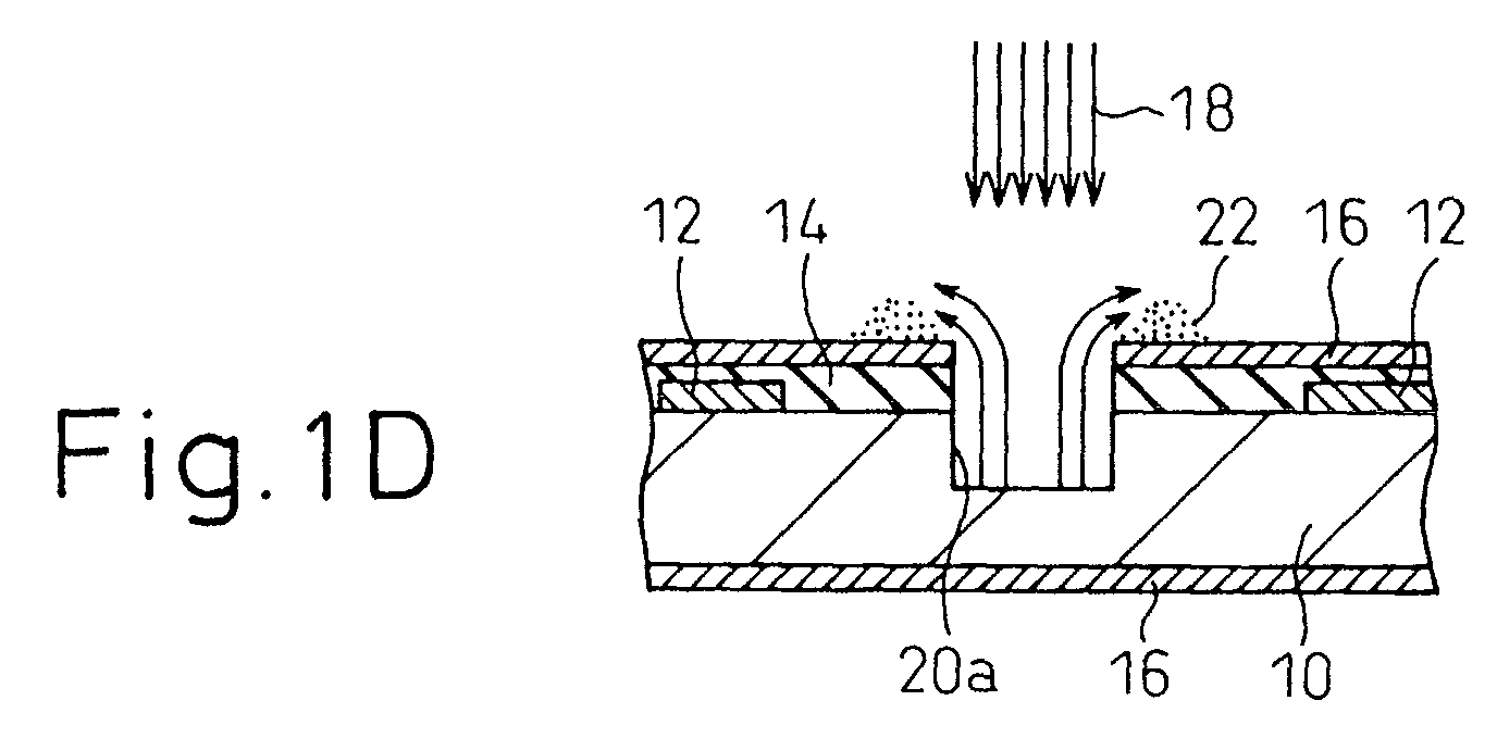
- laser beams 18 are irradiated to predetermined positions of the substrate 10 on its conductor formation side to form recess 20a (Fig. 1D).
- the substrate 10 is held by a vacuum onto a stage (not shown) and irradiation of the laser beam 18 is carried out, as explained previously with reference to Fig. 8.
- a YAG, an excimer, a carbon dioxide laser or the like can be used to generate the laser beam 18.
- the laser beam 18 When the laser beam 18 is thus irradiated to one side of the silicon substrate 10, the Ni plating film 16 and the SiO 2 film 14 at the irradiation portion are removed, and silicon (Si) of the substrate 10 is subsequently scattered by energy of the laser beam 18, thereby forming the recess 20a.
- the laser beam 18 is consecutively irradiated to the bottom of the recess 20a, the bottom of the recess 20a is scooped out and the recess 20a becomes gradually deeper.
- Silicon (Si) at the bottom of the recess 20a so scooped out is scattered away as a debris by the energy of the laser beam 18, is deposited on the portion in the proximity of the open periphery of the recess 20a, and forms a deposit (laser dross) 22.
- the laser dross 22 grows as the recess 20a becomes deeper.
- the recess 20a becomes gradually deeper, and at last the laser beam 18 breaks through the bottom of the recess 20a to thereby create a through-hole 20 (Fig. 1E).
- the laser dross 22 is formed in the proximity of the open periphery of the through-hole 20 on the one side of the substrate 10, and the deposit or debris 22a is deposited on the inner wall of the through-hole 20 as well as the proximity of its open periphery on the other side of the substrate 10.
- Such a debris 22a is formed as energy of the laser beam 18 scatters Si at bottom of the recess 20a to form the debris, and this debris is then deposited on the other side of the substrate 10 and on the inner wall of the through-hole 20.
- the laser dross 22 and the debris 22a are left as such, they peel from the substrate 10 in subsequent process steps, turn into foreign matter and are likely to invite the drop of reliability of the product.
- the Ni plating film 16 covering the entire surface of the substrate 10 inclusive of the top of the SiO 2 film 14 is peeled off, however, the laser dross 22 formed on the one side of the substrate 10 and the debris 22a deposited on the other side of the substrate 10 can be removed together (Fig. 1F).
- the Ni plating film 16 can be peeled by use of an Ni plating film peeling solution that is ordinarily used in the art.
- the debris 22a deposited on the inner wall surface of the through-hole 20 cannot be sufficiently removed even by the peeling solution for the Ni plating film 16. Therefore, the debris 22a is removed by use of a removing solution for the removal of the debris 22a on the other side of the substrate 10, such as a caustic potash (KOH) solution. In consequence, a clean through-hole 20 can be formed (Fig. 1G).
- a removing solution for the removal of the debris 22a on the other side of the substrate 10 such as a caustic potash (KOH) solution.
- KOH caustic potash
- a clean through-hole 20 can be formed (Fig. 1G).
- the conductor pattern 12 is not damaged because the SiO 2 film 14, as the protective film, protects it.
- the SiO 2 film 14 need not be peeled because it can be utilized as an insulating film in subsequent process steps.
- another SiO 2 film 14a thinner than the SiO 2 film 14 is formed on the entire surface of the substrate 10 inclusive of the inner wall surface of the through-hole 20 and the surface of the SiO 2 film 14 by means such as CVD (Fig. 1H). Further, electroless copper plating is applied to the surface of the SiO 2 film 14a to form a thin copper film 32a (Fig. 11).
- a resist pattern 34 is formed on the thin copper film 32a, after which electroplating of copper is carried out by using the resist pattern 34 as a mask and the thin copper film 32a as a power feed layer so as to form a copper layer 32 on the inner wall surface of the through-hole 20 and on both sides of the silicon substrate 10, to thereby form a through-hole-via and a conductor pattern (Fig. 1J).
- the resist pattern 34 is thereafter removed, and the exposed copper film 32a is etched away. There is thus obtained the silicon substrate 50 having the through-hole-via formed therein and the conductor pattern formed thereon (Fig. 1K).
- a plurality of silicon substrates 50a, 50b each having the through-hole-via and the conductor pattern are stacked with one another in such a manner that bumps 34 made of solder or gold are sandwiched between the substrates 50a, 50b and between the lowermost silicon substrate 50a and a mounting substrate 36 to establish electric connections among them, to thereby provide a three-dimensional multi-chip package (MCP), as shown in Fig. 2.
- MCP multi-chip package
- the method described above forms the through-hole-via by means of plating, but the via may be formed by filling an electrically conductive paste into the hole 20.
- the debris 22a is also deposited on the portion in the proximity of the open periphery of the through-hole 20 on the other side of the substrate 10, when the through-hole 20 is formed, as shown in the drawing.
- This phenomenon occurs when the substrate 10 is held by a vacuum on a stage and the laser beam 18 is irradiated onto the substrate 10, as shown in Fig. 8. More specifically, when the laser beam 18 breaks through the bottom of the recess 20a and creates the through-hole 20 opening to the other side of the substrate 10, the debris generated by the irradiation of the laser beam 18 to the bottom of the recess 20a is reflected by the surface of the stage and is deposited on the other side of the substrate 10.
- the debris inside the recess 20a is blown into the space portion 26 of the stage 24 and is prevented from being deposited to the other side of the substrate 10, when the laser beams 18 breaks the bottom of the recess portion 20a.
- a stage having debris reflection-prevention means that is equipped with a driver unit 42 for moving the substrate 10 along the upper surface of the stage 24, and with a controller unit 44 for controlling the driver unit 42 and moving the substrate 10 in such a fashion that the formation position of each of the through-holes 20 in the substrate 10 coincides with the space portion 26 of the stage 24.
- each through-hole 20 in the substrate 10 coincides with the space portion 26 of the stage 24
- small holes 25 formed in the stage 24 are connected to a vacuum so as to suck the substrate 10 to the stage, and the laser beam 18 is then irradiated to form the through-hole 20.
- the debris scattered by the irradiation of the laser beam 18 can enter the through-hole 20 that has already been formed.
- the laser beam 18 can be again irradiated into each of the through-holes 20 to remove the debris entering the through-holes 20, which can make cleaning after the formation of the through-holes 20 easy.
- a plurality of through-holes 20 are serially formed in the same direction (direction indicated by the arrow in Fig. 4A) when the through-holes are formed by the irradiation of the laser beam, heat is built up in some cases inside the substrate 10 even though the substrate 10 is covered with an Ni plating film to improve its heat dissipation property.
- a first through-hole 20(1) is formed in the substrate 10 through the irradiation of the laser beam, as shown in Fig. 4B.
- a second through-hole 20(2) is formed at a position that is not substantially affected by heat built up in the substrate 10 during the formation of the first through-hole 20(1).
- the broken lines in Fig. 4B respectively represent the extents to which the influences of heat due to the formation of the through-holes 20(1) and 20(2) spread. The problem of heat accumulation in the substrate 10 can be prevented when a next through-hole is formed at a position that is substantially free from the influences of heat of the through-holes formed previously.
- the start of the formation of the next through-hole is preferably retarded in time until heat of the through-hole 20 previously formed is dissipated.
- the through-hole 20 is formed by irradiating the laser beam 18 to one side (conductor pattern formation side) of the substrate having the conductor pattern 12 formed thereon. Therefore, the laser dross 22 is formed on the conductor pattern formation side of the substrate 10, and this side is contaminated much more than the other side of the substrate 10 on which the debris 22a is deposited.
- the laser dross 22 formed on the pattern formation side of the substrate 10 is removed when the Ni plating film 16 is peeled, but the portion in the proximity of the open periphery of the through-hole 20 having the laser dross 22 formed thereon is likely to be contaminated much more than the other portions.
- the through-hole can be formed in the substrate 10 without forming the laser dross 22 on the pattern formation side of the substrate 10 by irradiating the laser beam 18 to the other side of the substrate 10 on which the conductor pattern 12 is not formed.
- the laser beams 18 are irradiated in this way to the other side of the substrate 10 not having the pattern 12 formed thereon to form the through-hole, the influence of heat on the pattern 12 formed on the pattern formation side of the substrate can also be mitigated.
- through-holes 30a, 30b for the positioning on a frame member 28 surrounding the portion of the substrate 10 and later separated from it to leave the substrate 10, at the predetermined locations of the side thereof corresponding to the side of the substrate 10 to which the laser beam 18 is to be irradiated, as shown in Fig. 5B.
- the positions at which the through-holes 20 are to be formed can also be set immediately below the laser beam irradiation portion at the other side of the substrate 10.
- the stage 24 having the space portion 26 as the debris reflection-prevention means at position corresponding to the formation position of the through-hole in the substrate 10, as shown in Fig. 3.
- a plurality of through-holes 20 can be efficiently formed by using a debris reflection-prevention means having a driver unit 42 for moving the substrate 10 along the stage 24 and a controller unit 44 for controlling the driver unit 42 and moving the substrate 10 in such a fashion that the formation position of the each of through-holes 20 in the substrate 10 can be brought into conformity with the space portion 26 of the stage 24.
- the laser beam 18 is irradiated to one side of the substrate 10, as shown in Fig. 1D, and the irradiation of the laser beam 18 is stopped at the point at which a recess 20a having a predetermined depth is formed.
- the recess 20a can be formed in the substrate 10, as shown in Fig. 6A.
- the laser dross 22 is formed in the proximity of the open periphery of the recess 20a so formed, and the debris 22a is deposited to the inner wall surface and the bottom of the recess 20a.
- the laser dross 22 formed in the proximity of the open periphery of the recess portion 20a can be removed by immersing the substrate 10 into an Ni plating film peeling solution and peeling the Ni plating film 16 (Fig. 6B).
- the debris 22a deposited to the inner wall surface and the bottom of the recess 20a can be removed by, after the removal of the laser dross 22, immersing the substrate 10 into a removing solution for the laser dross 22, such as a caustic potash (KOH) solution, to provide a clean recess 20a (Fig. 6C).
- KOH caustic potash
- any of the embodiments of the invention described above it is possible to use a silicon nitride film, a diamond-like carbon film or a resin film, such as a polyimide film, in place of the SiO 2 film 14 as the protective film.
- Copper (Cu) or aluminum (Al) can be used as the metal plating film material besides nickel.
- the invention can improve the heat dissipation property of the silicon substrate during processing, can easily clean the deposit at the open periphery of the through-hole formed and the debris on the inner wall of the hole or recess, and can form a clean through-hole or recess.
- the invention can form a clean through-hole or recess in the silicon substrate by use of laser processing that is more economical than plasma processing, and can easily fabricate a three-dimensional MCP by stacking a plurality of semiconductor chips in a direction of thickness, for example.
Landscapes
- Internal Circuitry In Semiconductor Integrated Circuit Devices (AREA)
- Laser Beam Processing (AREA)
Abstract
Description
Claims (10)
- A method of forming a through-hole or a recess in a silicon substrate having a conductor pattern formed on one side thereof, comprising the steps of:forming a protective film for protecting the conductor pattern on the one side of the silicon substrate,forming, on substantially the entire surface of the silicon substrate inclusive of the top of the protective film, a metal plating film adhered to the protective film,irradiating a laser beam to a predetermined position of the silicon substrate covered with the protective film and with the metal plating film, to form a through-hole or a recess in the silicon substrate,peeling the metal plating film and removing debris on the metal plating film around the open periphery of the through-hole or the recess, which has been deposited thereon during the formation of the thorough-hole or the recess by the laser beam irradiation, andremoving a deposit on the inner wall of the thorough-hole or the recess, which has been deposited thereon during the formation of the thorough-hole or the recess by the laser beam irradiation, by use of a removing solution which does not damage the protective film.
- The method of claim 1, wherein the protective film is formed of silicon oxide, silicon nitride, diamond-like carbon, or a resin.
- The method of claim 1 or claim 2, wherein the metal plating film is formed of nickel, copper or aluminum.
- The method of any one of the preceding claims, wherein the deposit on the inner wall of the thorough-hole or the recess is removed by a solution of KOH, NaOH or HF.
- The method of any one of the preceding claims, wherein, in the case of the formation of a plurality of through-holes or recesses in the silicon substrate, following the formation of a previous through-hole or recess, a subsequent through-hole or recess is formed at a location of the substrate, the location being selected so that heat generated by the irradiation of the laser beam to the substrate for the formation of the previous through-hole or recess is not substantially accumulated in the substrate during the formation of the subsequent through-hole or recess.
- The method of any one of the preceding claims, wherein in the case of the formation of a plurality of through-holes or recesses in the silicon substrate, following the formation of a previous through-hole or recess, a subsequent through-hole or recess is formed at a time interval between the formations of the previous and subsequent through-holes or recesses, the time interval being selected so that heat generated by the irradiation of the laser beam to the substrate for the formation of the previous through-hole or recess is not substantially accumulated in the substrate during the formation of the subsequent through-hole or recess.
- The method of any one of the preceding claims, wherein, to prevent the debris from being reflected by the surface of a stage, on which the silicon substrate is positioned for the formation of the through-hole, and from depositing on the silicon substrate, at the time when the laser beam penetrates through the silicon substrate to create the through-hole, a stage having debris reflection-prevention means is used.
- The method of claim 7, wherein the stage has a hole piercing through it at a location thereof at which the through-hole is to be created.
- The method according to any one of the preceding claims, wherein, after the formation of a plurality of through-holes, the deposit within the formed through-holes is removed by irradiating the laser beam into the respective through-holes.
- The method of any one of the preceding claims, wherein, in the case of the formation of the through-hole, the laser beam is irradiated from the other side of the silicon substrate, not having the conductor pattern, to form the through-hole.
Applications Claiming Priority (2)
| Application Number | Priority Date | Filing Date | Title |
|---|---|---|---|
| JP2001316762 | 2001-10-15 | ||
| JP2001316762A JP3875867B2 (en) | 2001-10-15 | 2001-10-15 | Method for forming holes in silicon substrate |
Publications (3)
| Publication Number | Publication Date |
|---|---|
| EP1302979A2 true EP1302979A2 (en) | 2003-04-16 |
| EP1302979A3 EP1302979A3 (en) | 2004-03-24 |
| EP1302979B1 EP1302979B1 (en) | 2007-07-25 |
Family
ID=19134721
Family Applications (1)
| Application Number | Title | Priority Date | Filing Date |
|---|---|---|---|
| EP02256928A Expired - Lifetime EP1302979B1 (en) | 2001-10-15 | 2002-10-07 | Method of forming through-hole or recess in silicon substrate |
Country Status (4)
| Country | Link |
|---|---|
| US (1) | US6670269B2 (en) |
| EP (1) | EP1302979B1 (en) |
| JP (1) | JP3875867B2 (en) |
| CN (1) | CN1265438C (en) |
Cited By (2)
| Publication number | Priority date | Publication date | Assignee | Title |
|---|---|---|---|---|
| CN111485239A (en) * | 2019-01-29 | 2020-08-04 | 江苏三超金刚石工具有限公司 | Chemical deplating liquid for deplating nickel layer on surface of diamond and deplating method thereof |
| CN114464525A (en) * | 2020-11-09 | 2022-05-10 | 华为技术有限公司 | Method for processing diamond film and three-dimensional integrated circuit |
Families Citing this family (43)
| Publication number | Priority date | Publication date | Assignee | Title |
|---|---|---|---|---|
| US6908856B2 (en) * | 2003-04-03 | 2005-06-21 | Interuniversitair Microelektronica Centrum (Imec) | Method for producing electrical through hole interconnects and devices made thereof |
| US7345350B2 (en) * | 2003-09-23 | 2008-03-18 | Micron Technology, Inc. | Process and integration scheme for fabricating conductive components, through-vias and semiconductor components including conductive through-wafer vias |
| US7101792B2 (en) * | 2003-10-09 | 2006-09-05 | Micron Technology, Inc. | Methods of plating via interconnects |
| US7358186B2 (en) * | 2003-12-12 | 2008-04-15 | Lam Research Corporation | Method and apparatus for material deposition in semiconductor fabrication |
| US7316063B2 (en) * | 2004-01-12 | 2008-01-08 | Micron Technology, Inc. | Methods of fabricating substrates including at least one conductive via |
| US6943106B1 (en) * | 2004-02-20 | 2005-09-13 | Micron Technology, Inc. | Methods of fabricating interconnects for semiconductor components including plating solder-wetting material and solder filling |
| US7354863B2 (en) * | 2004-03-19 | 2008-04-08 | Micron Technology, Inc. | Methods of selectively removing silicon |
| JP4528100B2 (en) * | 2004-11-25 | 2010-08-18 | 新光電気工業株式会社 | Semiconductor device and manufacturing method thereof |
| JP4977432B2 (en) * | 2006-10-17 | 2012-07-18 | 株式会社ディスコ | Laser processing method of gallium arsenide wafer |
| WO2008123075A1 (en) * | 2007-03-27 | 2008-10-16 | Advantest Corporation | Through-etching process and method for producing contactor |
| TW200915505A (en) * | 2007-09-29 | 2009-04-01 | Kinik Co | Packaging carrier with high heat-dissipation and method for manufacturing the same |
| DE102008006745B3 (en) * | 2008-01-30 | 2009-10-08 | Siltronic Ag | Method for producing a semiconductor structure |
| JP5147779B2 (en) | 2009-04-16 | 2013-02-20 | 新光電気工業株式会社 | Wiring board manufacturing method and semiconductor package manufacturing method |
| US7994062B2 (en) * | 2009-10-30 | 2011-08-09 | Sachem, Inc. | Selective silicon etch process |
| TWI392069B (en) * | 2009-11-24 | 2013-04-01 | 日月光半導體製造股份有限公司 | Package structure and packaging process |
| US8455349B2 (en) * | 2010-04-28 | 2013-06-04 | Headway Technologies, Inc. | Layered chip package and method of manufacturing same |
| TWI446420B (en) | 2010-08-27 | 2014-07-21 | 日月光半導體製造股份有限公司 | Carrier separation method for semiconductor process |
| TWI445152B (en) | 2010-08-30 | 2014-07-11 | 日月光半導體製造股份有限公司 | Semiconductor structure and manufacturing method thereof |
| US9007273B2 (en) | 2010-09-09 | 2015-04-14 | Advances Semiconductor Engineering, Inc. | Semiconductor package integrated with conformal shield and antenna |
| TWI434387B (en) | 2010-10-11 | 2014-04-11 | 日月光半導體製造股份有限公司 | Semiconductor device having via hole and package structure of semiconductor device having via hole and manufacturing method thereof |
| TWI527174B (en) | 2010-11-19 | 2016-03-21 | 日月光半導體製造股份有限公司 | Package structure with semiconductor components |
| TWI445155B (en) | 2011-01-06 | 2014-07-11 | 日月光半導體製造股份有限公司 | Stacked package structure and manufacturing method thereof |
| US8853819B2 (en) | 2011-01-07 | 2014-10-07 | Advanced Semiconductor Engineering, Inc. | Semiconductor structure with passive element network and manufacturing method thereof |
| WO2013058169A1 (en) * | 2011-10-20 | 2013-04-25 | 旭硝子株式会社 | Method for forming through holes in insulating substrate and method for manufacturing insulating substrate for interposer |
| US8541883B2 (en) | 2011-11-29 | 2013-09-24 | Advanced Semiconductor Engineering, Inc. | Semiconductor device having shielded conductive vias |
| US8975157B2 (en) | 2012-02-08 | 2015-03-10 | Advanced Semiconductor Engineering, Inc. | Carrier bonding and detaching processes for a semiconductor wafer |
| US8963316B2 (en) | 2012-02-15 | 2015-02-24 | Advanced Semiconductor Engineering, Inc. | Semiconductor device and method for manufacturing the same |
| US8786060B2 (en) | 2012-05-04 | 2014-07-22 | Advanced Semiconductor Engineering, Inc. | Semiconductor package integrated with conformal shield and antenna |
| US9153542B2 (en) | 2012-08-01 | 2015-10-06 | Advanced Semiconductor Engineering, Inc. | Semiconductor package having an antenna and manufacturing method thereof |
| US8937387B2 (en) | 2012-11-07 | 2015-01-20 | Advanced Semiconductor Engineering, Inc. | Semiconductor device with conductive vias |
| US8952542B2 (en) | 2012-11-14 | 2015-02-10 | Advanced Semiconductor Engineering, Inc. | Method for dicing a semiconductor wafer having through silicon vias and resultant structures |
| US9406552B2 (en) | 2012-12-20 | 2016-08-02 | Advanced Semiconductor Engineering, Inc. | Semiconductor device having conductive via and manufacturing process |
| US8841751B2 (en) | 2013-01-23 | 2014-09-23 | Advanced Semiconductor Engineering, Inc. | Through silicon vias for semiconductor devices and manufacturing method thereof |
| WO2014130883A2 (en) | 2013-02-22 | 2014-08-28 | Allosource | Cartilage mosaic compositions and methods |
| US9978688B2 (en) | 2013-02-28 | 2018-05-22 | Advanced Semiconductor Engineering, Inc. | Semiconductor package having a waveguide antenna and manufacturing method thereof |
| US9089268B2 (en) | 2013-03-13 | 2015-07-28 | Advanced Semiconductor Engineering, Inc. | Neural sensing device and method for making the same |
| KR102312720B1 (en) | 2013-03-15 | 2021-10-13 | 알로소스 | Cell repopulated collagen matrix for soft tissue repair and regeneration |
| US9173583B2 (en) | 2013-03-15 | 2015-11-03 | Advanced Semiconductor Engineering, Inc. | Neural sensing device and method for making the same |
| US8987734B2 (en) | 2013-03-15 | 2015-03-24 | Advanced Semiconductor Engineering, Inc. | Semiconductor wafer, semiconductor process and semiconductor package |
| WO2015056349A1 (en) * | 2013-10-18 | 2015-04-23 | 三菱電機株式会社 | Machining table jig, manufacturing method of machining table jig, and laser processing method |
| US9545691B2 (en) * | 2013-12-23 | 2017-01-17 | Taiwan Semiconductor Manufacturing Company Limited | Method of removing waste of substrate and waste removing device thereof |
| CN108122820B (en) | 2016-11-29 | 2020-06-02 | 中芯国际集成电路制造(上海)有限公司 | Interconnect structure and method of making the same |
| JP7316730B2 (en) * | 2019-10-21 | 2023-07-28 | 株式会社ディスコ | Workpiece processing method |
Family Cites Families (23)
| Publication number | Priority date | Publication date | Assignee | Title |
|---|---|---|---|---|
| JPS5643611B2 (en) * | 1973-03-22 | 1981-10-14 | ||
| JPS5388568A (en) * | 1977-01-13 | 1978-08-04 | Nec Corp | Laser scribing apparatus |
| JPS5388567A (en) * | 1977-01-13 | 1978-08-04 | Nec Corp | Laser scribing apparatus |
| US4437109A (en) * | 1980-11-07 | 1984-03-13 | General Electric Company | Silicon-on-sapphire body with conductive paths therethrough |
| US4445978A (en) * | 1983-03-09 | 1984-05-01 | Rca Corporation | Method for fabricating via connectors through semiconductor wafers |
| JPS6028991U (en) * | 1983-08-02 | 1985-02-27 | 日本電気株式会社 | Laser processing equipment |
| JPS62101390A (en) * | 1985-10-25 | 1987-05-11 | Olympus Optical Co Ltd | Highly fine laser beam machining material and its processing |
| JPS62142486U (en) * | 1985-11-12 | 1987-09-08 | ||
| US5493096A (en) * | 1994-05-10 | 1996-02-20 | Grumman Aerospace Corporation | Thin substrate micro-via interconnect |
| US5631190A (en) * | 1994-10-07 | 1997-05-20 | Cree Research, Inc. | Method for producing high efficiency light-emitting diodes and resulting diode structures |
| US5646067A (en) * | 1995-06-05 | 1997-07-08 | Harris Corporation | Method of bonding wafers having vias including conductive material |
| JP2871636B2 (en) * | 1996-11-29 | 1999-03-17 | 日本電気株式会社 | LSI module and manufacturing method thereof |
| DE69737262T2 (en) * | 1997-11-26 | 2007-11-08 | Stmicroelectronics S.R.L., Agrate Brianza | A method of manufacturing a front-to-back via in micro-integrated circuits |
| JP3810204B2 (en) * | 1998-03-19 | 2006-08-16 | 三菱電機株式会社 | Semiconductor device manufacturing method and semiconductor device |
| JP2000052074A (en) * | 1998-08-06 | 2000-02-22 | Shinozaki Seisakusho:Kk | Laser processing method, laser processing material, grain selecter, and head part of ink jet printer |
| KR100379350B1 (en) * | 1998-12-16 | 2003-04-08 | 세이코 엡슨 가부시키가이샤 | Semiconductor chip, semiconductor device, circuit board and electronic equipment and production methods for them |
| JP2000246475A (en) * | 1999-02-25 | 2000-09-12 | Seiko Epson Corp | Processing method by laser beam |
| JP2000246474A (en) * | 1999-02-25 | 2000-09-12 | Seiko Epson Corp | Processing method by laser beam |
| JP4547728B2 (en) * | 1999-03-29 | 2010-09-22 | ソニー株式会社 | Semiconductor device and manufacturing method thereof |
| JP3775129B2 (en) * | 1999-09-21 | 2006-05-17 | セイコーエプソン株式会社 | Semiconductor chip connection method |
| JP3750444B2 (en) * | 1999-10-22 | 2006-03-01 | セイコーエプソン株式会社 | Manufacturing method of semiconductor device |
| TW490820B (en) * | 2000-10-04 | 2002-06-11 | Advanced Semiconductor Eng | Heat dissipation enhanced ball grid array package |
| JP3817453B2 (en) * | 2001-09-25 | 2006-09-06 | 新光電気工業株式会社 | Semiconductor device |
-
2001
- 2001-10-15 JP JP2001316762A patent/JP3875867B2/en not_active Expired - Fee Related
-
2002
- 2002-10-07 EP EP02256928A patent/EP1302979B1/en not_active Expired - Lifetime
- 2002-10-08 US US10/266,730 patent/US6670269B2/en not_active Expired - Lifetime
- 2002-10-15 CN CNB02146233XA patent/CN1265438C/en not_active Expired - Fee Related
Cited By (2)
| Publication number | Priority date | Publication date | Assignee | Title |
|---|---|---|---|---|
| CN111485239A (en) * | 2019-01-29 | 2020-08-04 | 江苏三超金刚石工具有限公司 | Chemical deplating liquid for deplating nickel layer on surface of diamond and deplating method thereof |
| CN114464525A (en) * | 2020-11-09 | 2022-05-10 | 华为技术有限公司 | Method for processing diamond film and three-dimensional integrated circuit |
Also Published As
| Publication number | Publication date |
|---|---|
| JP2003124154A (en) | 2003-04-25 |
| EP1302979A3 (en) | 2004-03-24 |
| US6670269B2 (en) | 2003-12-30 |
| EP1302979B1 (en) | 2007-07-25 |
| JP3875867B2 (en) | 2007-01-31 |
| US20030073299A1 (en) | 2003-04-17 |
| CN1265438C (en) | 2006-07-19 |
| CN1412821A (en) | 2003-04-23 |
Similar Documents
| Publication | Publication Date | Title |
|---|---|---|
| EP1302979B1 (en) | Method of forming through-hole or recess in silicon substrate | |
| KR100741864B1 (en) | Method for manufacturing semiconductor device | |
| KR100999907B1 (en) | How to Plug Through Holes in Silicon Substrates | |
| KR100658547B1 (en) | Semiconductor device and manufacturing method thereof | |
| KR100725565B1 (en) | Manufacturing Method of Semiconductor Device | |
| US7211899B2 (en) | Circuit substrate and method for fabricating the same | |
| KR100608184B1 (en) | Semiconductor device and method for manufacturing the same | |
| CN116490971A (en) | Package structure with built-in EMI shielding | |
| CN100383938C (en) | Semiconductor device and method for manufacturing the same | |
| US5138439A (en) | Semiconductor device | |
| KR20060049324A (en) | Semiconductor device and manufacturing method thereof | |
| KR100608186B1 (en) | Method of manufacturing semiconductor device | |
| EP2087516A2 (en) | Wafer-level fabrication of lidded chips with electrodeposited dielectric coating | |
| KR100847933B1 (en) | Protective layer during scribing | |
| KR100689132B1 (en) | Manufacturing Method of Semiconductor Device | |
| KR20110107989A (en) | Method of forming a laminated semiconductor package | |
| JP4181807B2 (en) | Laser processing method | |
| KR100927778B1 (en) | Semiconductor Package Manufacturing Method | |
| US20240347477A1 (en) | Method for forming a shielding layer over a semiconductor package with reduced metal burrs | |
| US7071571B2 (en) | Semiconductor component having a plastic housing and methods for its production | |
| KR100593211B1 (en) | Wafer-Through Electrode Manufacturing Method | |
| KR100785731B1 (en) | A method of forming openings or cavities in a substrate for receiving electronic components | |
| KR20100053828A (en) | Methods of manufacturing a bump with improved the performance of connection between bonding pad metal | |
| KR101091243B1 (en) | Manufacturing method of printed circuit board | |
| JPH0992675A (en) | Semiconductor device and manufacturing method thereof |
Legal Events
| Date | Code | Title | Description |
|---|---|---|---|
| PUAI | Public reference made under article 153(3) epc to a published international application that has entered the european phase |
Free format text: ORIGINAL CODE: 0009012 |
|
| AK | Designated contracting states |
Designated state(s): AT BE BG CH CY CZ DE DK EE ES FI FR GB GR IE IT LI LU MC NL PT SE SK TR |
|
| AX | Request for extension of the european patent |
Extension state: AL LT LV MK RO SI |
|
| PUAL | Search report despatched |
Free format text: ORIGINAL CODE: 0009013 |
|
| RIC1 | Information provided on ipc code assigned before grant |
Ipc: 7H 01L 23/48 B Ipc: 7H 01L 21/3065 A Ipc: 7H 01L 21/768 B |
|
| AK | Designated contracting states |
Kind code of ref document: A3 Designated state(s): AT BE BG CH CY CZ DE DK EE ES FI FR GB GR IE IT LI LU MC NL PT SE SK TR |
|
| AX | Request for extension of the european patent |
Extension state: AL LT LV MK RO SI |
|
| 17P | Request for examination filed |
Effective date: 20040914 |
|
| AKX | Designation fees paid |
Designated state(s): GB |
|
| REG | Reference to a national code |
Ref country code: DE Ref legal event code: 8566 |
|
| GRAP | Despatch of communication of intention to grant a patent |
Free format text: ORIGINAL CODE: EPIDOSNIGR1 |
|
| GRAS | Grant fee paid |
Free format text: ORIGINAL CODE: EPIDOSNIGR3 |
|
| GRAA | (expected) grant |
Free format text: ORIGINAL CODE: 0009210 |
|
| AK | Designated contracting states |
Kind code of ref document: B1 Designated state(s): GB |
|
| REG | Reference to a national code |
Ref country code: GB Ref legal event code: FG4D |
|
| PLBE | No opposition filed within time limit |
Free format text: ORIGINAL CODE: 0009261 |
|
| STAA | Information on the status of an ep patent application or granted ep patent |
Free format text: STATUS: NO OPPOSITION FILED WITHIN TIME LIMIT |
|
| 26N | No opposition filed |
Effective date: 20080428 |
|
| PGFP | Annual fee paid to national office [announced via postgrant information from national office to epo] |
Ref country code: GB Payment date: 20161005 Year of fee payment: 15 |
|
| GBPC | Gb: european patent ceased through non-payment of renewal fee |
Effective date: 20171007 |
|
| PG25 | Lapsed in a contracting state [announced via postgrant information from national office to epo] |
Ref country code: GB Free format text: LAPSE BECAUSE OF NON-PAYMENT OF DUE FEES Effective date: 20171007 |