EP1296145A1 - Conductive contact - Google Patents
Conductive contact Download PDFInfo
- Publication number
- EP1296145A1 EP1296145A1 EP01943857A EP01943857A EP1296145A1 EP 1296145 A1 EP1296145 A1 EP 1296145A1 EP 01943857 A EP01943857 A EP 01943857A EP 01943857 A EP01943857 A EP 01943857A EP 1296145 A1 EP1296145 A1 EP 1296145A1
- Authority
- EP
- European Patent Office
- Prior art keywords
- conductive contact
- contact member
- conductive
- coil spring
- solder
- Prior art date
- Legal status (The legal status is an assumption and is not a legal conclusion. Google has not performed a legal analysis and makes no representation as to the accuracy of the status listed.)
- Granted
Links
Images





Classifications
-
- H—ELECTRICITY
- H01—ELECTRIC ELEMENTS
- H01R—ELECTRICALLY-CONDUCTIVE CONNECTIONS; STRUCTURAL ASSOCIATIONS OF A PLURALITY OF MUTUALLY-INSULATED ELECTRICAL CONNECTING ELEMENTS; COUPLING DEVICES; CURRENT COLLECTORS
- H01R33/00—Coupling devices specially adapted for supporting apparatus and having one part acting as a holder providing support and electrical connection via a counterpart which is structurally associated with the apparatus, e.g. lamp holders; Separate parts thereof
- H01R33/74—Devices having four or more poles, e.g. holders for compact fluorescent lamps
- H01R33/76—Holders with sockets, clips, or analogous contacts adapted for axially-sliding engagement with parallely-arranged pins, blades, or analogous contacts on counterpart, e.g. electronic tube socket
-
- G—PHYSICS
- G01—MEASURING; TESTING
- G01R—MEASURING ELECTRIC VARIABLES; MEASURING MAGNETIC VARIABLES
- G01R1/00—Details of instruments or arrangements of the types included in groups G01R5/00 - G01R13/00 and G01R31/00
- G01R1/02—General constructional details
- G01R1/06—Measuring leads; Measuring probes
- G01R1/067—Measuring probes
- G01R1/06711—Probe needles; Cantilever beams; "Bump" contacts; Replaceable probe pins
- G01R1/06716—Elastic
- G01R1/06722—Spring-loaded
-
- G—PHYSICS
- G01—MEASURING; TESTING
- G01R—MEASURING ELECTRIC VARIABLES; MEASURING MAGNETIC VARIABLES
- G01R1/00—Details of instruments or arrangements of the types included in groups G01R5/00 - G01R13/00 and G01R31/00
- G01R1/02—General constructional details
- G01R1/06—Measuring leads; Measuring probes
- G01R1/067—Measuring probes
- G01R1/06711—Probe needles; Cantilever beams; "Bump" contacts; Replaceable probe pins
- G01R1/06716—Elastic
-
- H—ELECTRICITY
- H01—ELECTRIC ELEMENTS
- H01R—ELECTRICALLY-CONDUCTIVE CONNECTIONS; STRUCTURAL ASSOCIATIONS OF A PLURALITY OF MUTUALLY-INSULATED ELECTRICAL CONNECTING ELEMENTS; COUPLING DEVICES; CURRENT COLLECTORS
- H01R12/00—Structural associations of a plurality of mutually-insulated electrical connecting elements, specially adapted for printed circuits, e.g. printed circuit boards [PCB], flat or ribbon cables, or like generally planar structures, e.g. terminal strips, terminal blocks; Coupling devices specially adapted for printed circuits, flat or ribbon cables, or like generally planar structures; Terminals specially adapted for contact with, or insertion into, printed circuits, flat or ribbon cables, or like generally planar structures
- H01R12/50—Fixed connections
- H01R12/51—Fixed connections for rigid printed circuits or like structures
- H01R12/52—Fixed connections for rigid printed circuits or like structures connecting to other rigid printed circuits or like structures
-
- H—ELECTRICITY
- H05—ELECTRIC TECHNIQUES NOT OTHERWISE PROVIDED FOR
- H05K—PRINTED CIRCUITS; CASINGS OR CONSTRUCTIONAL DETAILS OF ELECTRIC APPARATUS; MANUFACTURE OF ASSEMBLAGES OF ELECTRICAL COMPONENTS
- H05K7/00—Constructional details common to different types of electric apparatus
- H05K7/02—Arrangements of circuit components or wiring on supporting structure
- H05K7/10—Plug-in assemblages of components, e.g. IC sockets
- H05K7/1053—Plug-in assemblages of components, e.g. IC sockets having interior leads
- H05K7/1061—Plug-in assemblages of components, e.g. IC sockets having interior leads co-operating by abutting
- H05K7/1069—Plug-in assemblages of components, e.g. IC sockets having interior leads co-operating by abutting with spring contact pieces
-
- G—PHYSICS
- G01—MEASURING; TESTING
- G01R—MEASURING ELECTRIC VARIABLES; MEASURING MAGNETIC VARIABLES
- G01R1/00—Details of instruments or arrangements of the types included in groups G01R5/00 - G01R13/00 and G01R31/00
- G01R1/02—General constructional details
- G01R1/04—Housings; Supporting members; Arrangements of terminals
- G01R1/0408—Test fixtures or contact fields; Connectors or connecting adaptors; Test clips; Test sockets
- G01R1/0433—Sockets for IC's or transistors
- G01R1/0441—Details
- G01R1/0466—Details concerning contact pieces or mechanical details, e.g. hinges or cams; Shielding
-
- G—PHYSICS
- G01—MEASURING; TESTING
- G01R—MEASURING ELECTRIC VARIABLES; MEASURING MAGNETIC VARIABLES
- G01R1/00—Details of instruments or arrangements of the types included in groups G01R5/00 - G01R13/00 and G01R31/00
- G01R1/02—General constructional details
- G01R1/04—Housings; Supporting members; Arrangements of terminals
- G01R1/0408—Test fixtures or contact fields; Connectors or connecting adaptors; Test clips; Test sockets
- G01R1/0433—Sockets for IC's or transistors
- G01R1/0483—Sockets for unleaded IC's having matrix type contact fields, e.g. BGA or PGA devices; Sockets for unpackaged, naked chips
-
- H—ELECTRICITY
- H01—ELECTRIC ELEMENTS
- H01R—ELECTRICALLY-CONDUCTIVE CONNECTIONS; STRUCTURAL ASSOCIATIONS OF A PLURALITY OF MUTUALLY-INSULATED ELECTRICAL CONNECTING ELEMENTS; COUPLING DEVICES; CURRENT COLLECTORS
- H01R13/00—Details of coupling devices of the kinds covered by groups H01R12/70 or H01R24/00 - H01R33/00
- H01R13/02—Contact members
- H01R13/22—Contacts for co-operating by abutting
- H01R13/24—Contacts for co-operating by abutting resilient; resiliently-mounted
- H01R13/2407—Contacts for co-operating by abutting resilient; resiliently-mounted characterized by the resilient means
- H01R13/2421—Contacts for co-operating by abutting resilient; resiliently-mounted characterized by the resilient means using coil springs
Definitions
- the present invention relates to a conductive contact member suitable for testing and other applications in the field of semiconductor devices.
- a conductive contact member when the contact part of the object to be tested (such as a terminal of a semiconductor device) is made of solder or covered by solder, repeated application of the conductive contact member onto such terminals causes a deposition of solder on the tip of the conductive contact member which may be in the form of a needle member or a coil.
- a conductive contact member is surface processed by gold plating (which is added with 0.3 to 4% of cobalt, for instance) to ensure stable electric properties and a low electric resistance.
- gold plating which is added with 0.3 to 4% of cobalt, for instance
- the electric resistance in the electric path of the conductive contact member deviates from the expected range, and the accuracy of the test may be impaired. Therefore, it was necessary to replace the conductive contact member before the accuracy of the test drops below a prescribed level. As a result, the conductive contact member had to be replaced for cleaning so frequently that the efficiency of the test line was impaired, and the maintenance cost increased.
- a primary object of the present invention is to provide a conductive contact member which is required to be replaced due to solder deposition less frequently than the conventional conductive contact member.
- a second object of the present invention is to provide a conductive contact member which demonstrates a low electric resistance over a prolonged period of time, and thereby provides a longer service life than the conventional conductive contact member.
- a third object of the present invention is to provide a conductive contact member having a contact portion which is resistant to solder deposition.
- a conductive contact member for establishing an electric contact by being applied to an object to be contacted, comprising a layer of highly electrically conductive material resistant to solder deposition formed at least over a conductive contact part of the conductive contact member.
- the layer of highly electrically conductive material may be formed preferably by electroplating, but also by other processes which include, not exclusively, electroless plating, sputtering, PVD, CVD and thermal spraying.
- the highly electrically conductive material preferably consists essentially of gold added with 0.01% to 8% of silver.
- the conductive contact member may be in the form of a coil spring or needle member or rod member which may have either a pointed end or flat end.
- the deposition of solder to the conductive contact part is minimized even when it is repeatedly applied to objects to be contacted, and the frequency of replacing the conductive contact part can be reduced.
- the base material for the conductive contact member may consist of inexpensive material having favorable mechanical properties such as steel, the conductive contact member can continue to demonstrate a low electric resistance even after a large number of test cycles or a long service period in a stable manner.
- FIG. 1 is an enlarged sectional side view of an essential part of a conductive contact member 3 used in a contact probe head for contacting semiconductor devices embodying the present invention.
- an electrically insulating holder 1 is formed by a pair of plastic insulating plate members 1a and 1b placed closely one over the other in an integral manner, and through holes 2 (only one of them is shown in the drawing) are passed across the thickness of the holder 1.
- a conductive contact member 3 in the form of a coil spring is coaxially received in each of the through holes 2.
- the through hole 2 is provided with a straight main section having a constant diameter and a prescribed length at an axially intermediate part thereof, and a pair of tapered sections 2a each having a narrower end opening toward the upper or lower end of the holder 1 as seen in the drawing.
- the narrowed open end of each tapered section 2a communicates with the exterior of the through hole 2 via a small diameter section 2b having a constant small diameter and a prescribed length.
- the conductive contact member 3 in the form of a coil spring is formed by winding a wire made of spring material such as steel into a coil, and comprises a coil spring section 4 wound at a prescribed pitch and received in the straight section formed in the intermediate part of the through hole 2 with a certain radial play, and a pair of electrode pin sections 5a and 5b serving as conductive contact parts.
- Each electrode pin section 5a, 5b consists of a plurality of turns of the coil wire extending from the coil spring section 4 and having the same diameter as the coil spring section 4, and a closely would tapered section extending therefrom to a coil end.
- each electrode pin section 5a, 5b is substantially complementary in shape to the tapered section 2a of the through hole 2, and has an outer end which has a smaller diameter than the inner diameter of the small diameter section 2b so as to be able to project outwardly out of the small diameter section 2b.
- the conductive contact member 3 in the form of a coil spring is received in the through hole 2 with the coil spring section 4 compressed.
- the insulating plate members 1a and 1b are placed one over the other with the electrode pin sections 5a and 5b received in the corresponding parts of the through hole 2 so that the conductive contact member 3 in the form of a coil spring is assembled into the insulating plate 3 with a certain pre-stress applied to the coil spring section 4.
- the outer ends of the electrode pin sections 5a and 5b are each guided by and into the corresponding tapered section 2a of the through hole 2 simply by placing the outer end of the electrode pin section 5a, 5b in the opposing open ends of the through hole 2. Therefore, the assembly work is substantially simplified as compared to the case of a conductive contact member in the form of a needle member which is required to be passed into a support hole without any such guiding action during the assembly process.
- each tapered electrode pin section 5a, 5b causes each tapered electrode pin section 5a, 5b to abut the complementary tapered surface of the corresponding tapered section 2a of the through hole 2 so that the conductive contact member 3 is prevented from being dislodged from the through hole 2 while the variations in the lateral position of the tip of each conductive contact member 3 is minimized.
- each electrode pin section 5a, 5b of each conductive contact member 3 projects out of the corresponding through hole 2 by a prescribed length under a rest condition.
- a conductive contact member 3 can be used, in a contact probe for instance, to contact a terminal of a semiconductor device such as a solder ball 7a of a BGA7.
- the conductive contact member 3 By applying a preload to the conductive contact member 3 in the form of a coil spring, it becomes possible to minimize the variations in the contact load due to the variations in the deflection stroke arising from the variations in the elevation of the object to be contacted (such as the circuit pattern 6a and terminal 7a) to which the conductive contact member 3 is applied.
- Figures 2 to 4 show the mode of forming the conductive contact member 3 in the form of a coil spring according to the present invention.
- gold added with 0.01% to 8% of silver is plated over the surface of a coil wire 3a made of spring material such as steel as mentioned earlier as a surface process of forming a highly electroconductive layer, and a gold plate layer 8a added with silver is thereby formed over the entire outer surface of the coil wire 3a as illustrated in Figure 2.
- the gold-plated coil wire 3a is then subjected to a coiling process, and the coil spring section 4 and electrode pin sections 5a and 5b as illustrated in Figure 1 are formed.
- the coil wire 3a is closely wound in the electrode pin sections 5a and 5b as illustrated in Figure 3, and is additionally given with a pre-stress so that the adjacent turns of the coil wire 3a of the electrode pin sections 5a and 5b are pressed against one another.
- the axially opposing gold plate layers 8a added with silver each abut one another with a certain preload.
- the gold plate layer 8a added with silver was formed on the coil wire 3a before it is coiled.
- the material for the coil wire 3a can be freely selected without regard to its electric conductivity, and may consist of materials such as spring material which have favorably mechanical properties and are inexpensive.
- the mode of operation of the conductive contact member 3 in the form of a coil spring which is manufactured as described above is illustrated in Figure 5.
- the coil spring section 4 is necessary for resiliently applying the conductive contact member 3 onto the object to be contacted.
- the number of turns N of the coil spring is related the electric inductance H thereof according to the equation given below.
- H AN 2 /L where A is a coefficient, and L is the length of the coil spring. Therefore, for minimizing the inductance, it is essential to reduce N as much as possible. To this end, it is desired that the number of turn is 10 or less, but, more preferably, two or less as is the case with the illustrated embodiment.
- each electrode pin section 5a, 5b is closely wound, and generally covered by the second gold plate layer 8b added with silver in axially continuous manner, the electric conductive path in the electrode pin section extends in the axial direction of the coil spring. Therefore, even though the coil wire is turned into a coil, the electric current does not flow along a spiral path, and this contributes to the reduction in the electric resistance and inductance.
- the straight small diameter section 2b is formed between the outer end of the tapered section 2a of the through hole 2 and the exterior of the through hole 2, the tip of the tapered electrode pin section 5a, 5b is prevented from being caught by this part of the through hole 2. Also, because the provision of the straight small diameter section 2b ensures a substantial wall thickness to the peripheral part of the opening, the peripheral part of the open end of the straight small diameter section 2b is prevented from being damaged by an inadvertent contact with a terminal consisting of a solder ball 7a or the like.
- the electrode pin section 5a When testing a semiconductor device such as a BGA 7 by using such a conductive contact member, the electrode pin section 5a is repeatedly brought into contact with a number of BGAs 7 conveyed along a test line one by one as indicated by the arrow A in Figure 5. As a result of such repeated contacts with terminals 7a, a small portion of the solder on each terminal deposits on the electrode pin section 5a, and the amount of deposition increases with the number of contacts.
- the deposition of solder can be substantially reduced as compared with the conventional gold plating added with cobalt (0.3% to 4%).
- the conductive contact member according to the present invention was able to withstand more than 20,000 test cycles.
- the conductive contact member of the present invention was applied to a contact probe head in the foregoing embodiment, the conductive contact member of the present invention can also be used as electric sockets for semiconductor devices. In this case, the possible number of reuse of the socket can be substantially increased, and the durability of the socket can be enhanced.
- the conductive contact member according to the present invention is not limited to the conductive contact member 3 in the form of a coil spring, but may also consist of a conductive needle member 14 for a contact probe head 11. Such a conductive contact member 14 is described in the following.
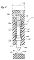
- Figure 6 is a schematic longitudinal sectional view of a contact probe head 11 employing the conductive contact member 14 embodying the present invention.
- the object to be tested typically includes a plurality of points to be contacted that need to be accessed simultaneously, and a large number of such conductive contact members 14 are arranged in parallel to one another. It can be also used as a sole conductive contact member 14 in a contact probe.
- a holder is formed by passing a support hole 13 across the thickness of an insulating plate member 12, and a conductive needle member 14 is coaxially received in the support hole 13.
- a compression coil spring 15 resiliently urges the conductive needle member 14 outwardly out of the support hole 13.
- a relay board 16 serving as signal exchanging means, and an electroconductive path 16a is formed integrally with the relay board 16 to conduct an electric signal across the thickness of the relay board 16.
- a test circuit board 19 is typically placed over the relay board 16 when the conductive contact member 14 is put to an actual use.
- the contact probe head can be readily adapted to different layout patterns of the object to be contacted.
- the conductive needle member 14 comprises a head 14a having a pointed end and adapted to contact an object to be contacted, a large diameter portion 14b provided on the inner end of the head 14a, and a stem portion 14c extending from the inner end of the large diameter portion 14b to the inner most end, all in a coaxial relationship.
- the support hole 13 receives the large diameter portion 14b of the conductive needle member 14 and the compression coil spring 15 coaxially wound around the stem portion 14c.
- the support hole 13 is provided with a small diameter portion 13a at an end facing away from the relay board 16 for axially slidably supporting only the head 14a, and a shoulder defined by the small diameter portion 13a of the support hole 13 engages the large diameter portion 14b to retain the conductive needle member 14 in the support hole 13.
- the projecting end of the head 14a consists of a pointed end so that an accurate contact may be established even when a small pad is required to be contacted.
- the terminal end of the head 14a may also take other forms depending on the shapes of the objects to be contacted, and may be provided with a flat end, instead of a pointed end, to be adapted to contact a solder ball, for instance.
- a gold plating added with 0.5% to 8% of silver is applied to the head 14a of the conductive needle member 14 in a similar manner as the previous embodiment so as to form a gold plate layer 18 added with silver as illustrated in Figure 7.
- the deposition of solder onto the conductive needle member 14 can be substantially reduced when contacting objects to be contacted, and the advantages mentioned above can be gained.
- the compression coil spring 15 wound around the stem portion 14c is assembled in a pre-compressed state between the large diameter portion 14b and relay board 16.
- a slightly enlarged boss portion 14d having a slightly larger outer diameter than the inner diameter of the compression coil spring 15 is formed in the part of the stem portion 14c adjacent to the large diameter portion 14b so that the coil end of the compression coil spring 15 may be resiliently wrapped around the boss portion 14d. Therefore, the compression coil spring 15 can be integrally combined with the conductive needle member 14 prior to placing the conductive needle member 14 in the support hole 13, and this simplifies the assembling process.
- the compression coil spring 15 can be joined with the boss portion 14d by resiliently wrapping around it as is the case with the illustrated embodiment, but may also be soldered to the boss portion to achieve a similar joining action. Also, a simple fitting engagement may be adequate if the required contact pressure can be achieved.
- the compression coil spring 15 is provided with a closely wound section 15a which remains in a closely wound state under the rest condition at an end facing the relay board 16 or the end corresponding to the retracting direction of the conductive needle member 14.
- the closely wound section 15a extends downwardly to a point where it slightly overlaps with the upper end of the stem portion 14c as seen in the drawing in the inoperative state illustrated in Figure 6.
- the compression coil spring 15 disposed in this fashion is provided with a coil end (lower end as seen in the drawing) fixedly attached to a boss portion 14d of the conductive needle member 14 formed adjacent to the large diameter portion 14b and another coil end (upper end as seen in the drawing) corresponding to the closely wound section 15a received in a recess formed in a part of the electric conductive path 16a of the relay board 16 facing the support hole 13 and abutting the bottom surface of the recess.
- the inner diameter of the compression coil spring 15 is slightly larger than the outer diameter of the stem portion 14c.
- the conductive needle member 14 may also be gold plated added with silver or otherwise surface processed (such as rhodium plating) not only at the head 14a but also over the entire surface.
- the conductive needle member 14 may be made of material (such as precious metal alloys and copper alloys) having a favorable electric property so as not to adversely affect the electric signal, and only the head may be subjected to the gold plating added with silver.
- the compression coil spring 15 is typically made of conductive material having a spring property such as steel, but may also be surface processed as mentioned above.
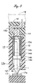
- the holder consisting of the insulating plate member 12 is lowered onto the object to be tested 17, and with the pointed end of each head 14a caused to abut the corresponding pad 17a and the compression coil spring 15 compressed, the conductive needle member 14 is brought into contact with the pad 17a with an adequate loading which enables it to penetrate an oxide film that may be formed on the surface of the pad 17a.
- the head 14a is formed with a gold plate layer mixed with silver which prohibits solder deposition, it is possible to favorably avoid the transfer of solder from the objects to be tested which the head 14a is brought into contact with.
- an electric signal flows from the pad 17a to the electric conductive path 16a via the conductive needle member 14 and the compression coil spring 15 as indicated by the arrow I shown in Figure 8. Because the inner diameter of the compression coil spring 15 is slightly larger than the outer diameter of the stem portion 14c, the compression of the coil spring 15 causes it to meander or curve like a snake within the support hole 13 so that the inner circumference of the closely wound section 15a engages the outer circumferential surface of the stem portion 14c.
- the closely wound section 15a consists of mutually contacting turns of the coil wire
- the electric signal which is transmitted from the conductive needle member 14 to the compression coil spring 15 is allowed to flow along the axial direction of the compression coil spring as shown in Figure 8, instead of flowing along a spiral path defined by the coil wire of coarsely wound turns, so that the electric inductance and resistance are minimized.
- the lower end of the compression coil spring 15 is wrapped around the boss portion 14d, and this provides an alternate or parallel electric path with respect to the electric path defined along the stem portion 14c. This also contributes to a stable and low resistance transmission of signals by the contact probe head.
- the free end of the stem portion 14c slightly overlaps with the closely wound section 15a. It is also possible to have them overlap each other over a greater length, or to do away with such an overlapping.
- the stem portion 14c is brought into contact with the closely wound section 15a so that the closely wound section 15a is brought into contact with the conductive needle member 14 without fail without regard to the variations in the height of the point to be contacted and the variations in the compressive deformation of the compression coil spring 15 for each conductive needle member 14.
- each conductive needle member consisted of a pointed conical end, but may also consist of a flat end as illustrated in Figure 9 if the object to be contacted consists of a solder ball 7a or the like.
- a gold plate layer added with silver 18' is formed over the surface of a cylindrical end portion of the head 14a' of a conductive contact member 14, and the end surface engages the solder ball 7a via the gold layer added with silver 18'.
- the conducive contact member embodying the present invention is not limited to those illustrated above.
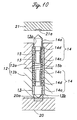
- a third embodiment of the present invention is described in the following with reference to Figure 10.
- the parts corresponding to those of the previous embodiments are denoted with like numerals without repeating the description of such parts.
- the conductive needle members 14 illustrated in Figure 10 are not provided with a part corresponding to the large diameter portion 14b of the previous embodiment, but is otherwise similar to the same.
- An end of a compression coil spring 15 is connected to the conductive needle member 14 by being wrapped around a boss portion 14d of the corresponding conductive needle member 14, and the other coil end is similarly connected to an identical and coaxially disposed conductive needle member 14 so as to form a contact probe head having a pair of moveable ends.
- the heads 14a of these conductive needle members 14 thus face away from each other.
- the holder 12 for defining a support hole 13 to receive the compression coil spring 15 and support the two conductive needle members 14 is formed by placing a pair of plastic plate members 12a and 12b one over the other.
- the upper and lower surfaces of the plate members 12a and 12b as seen in the drawing are each formed with a small diameter hole 13a, 13b which is more reduced in diameter than the remaining part of the support hole 13 but can slidably receive the cylindrical part of the corresponding head 14a.
- each conductive needle member 14 is prevented from coming off from the support hole 13 by the outer peripheral part of the compression coil spring 15 wrapped around the boss portion 14d engaging the shoulder defined between the support hole 13 and the corresponding small diameter hole 13a, 13b.
- a circuit board 20 such as a burn-in board is provided in a lower part as seen in the drawing, and one of the conductive needle members 14 is brought into contact with a circuit pattern 20a which is formed so as to be flush with the remaining surface of the circuit board 20.
- the contact probe head is moved toward the object to be tested 21 shown in an upper part of the drawing, and the other conductive needle member 14 is resiliently brought into contact with a test pad 21a of the object to be tested 21.
- both of the conductive needle members 14 are in a similar state to that of the lower conductive needle member 14 shown in the drawing.
- the electric signal is conducted from the test pad 21a to the upper conductive needle member 14, and is further conducted from the stem portion 14c of the upper conductive needle member 14 to the stem portion 14c of the lower conductive needle member 14 via the closely wound section 15b provided in an intermediate portion of the compression coil spring 15 before the electric signal is finally conducted from the lower conductive needle member 14 to the circuit pattern 20a.
- the conductive path passes through the closely wound section 15b of the compression coil spring 15, and extends linearly along the axial direction of the compression coil spring 15. Therefore, the increase in the electric inductance and resistance due to the high frequency signal flowing through a coarsely wound section along a spiral path can be avoided, and the electric inductance and resistance can be reduced.
- This embodiment allows the overall length of the assembly to be reduced at least by the length of the large diameter portion 14b, and such a simplification of the shape of the conductive needle member 14 contributes to the reduction in the component cost.
- the head 14a of the conductive needle member 14 is subjected to a gold plating added with silver in a similar way as the previous embodiments. Because the head 14a is provided with a gold plate layer added with silver which is resistant to solder deposition, deposition of solder onto the head 14a can be avoided even after a repeated contacts with the objects to be tested.
- a fourth embodiment as illustrated in Figure 11 is also possible.
- the parts corresponding to those of the previous embodiment are denoted with like numerals without repeating the description of such parts.
- only one conductive needle member 14 is used as opposed to the embodiment illustrated in Figure 10 having two moveable ends, and a coil end of a compression coil spring 15 is used as a conductive contact member instead.
- the coil end of the compression coil spring 15 which is not associated with a separate conductive needle member is provided with a closely wound section 15a which includes a straight section adjacent to the coarsely wound section or the main section of the compression coil spring and having about the same diameter as the main section, a tapered section having a larger end connected to the straight section, and a straight small diameter section 15c connected to the smaller end of the tapered section.
- the straight small diameter section 15c is brought into contact with the circuit pattern 20a.
- the compression coil spring 15 is closely wound from a point slightly overlapping with the stem portion 14c of the conductive needle member 14 to the outer end defined by the straight small diameter section 15c.
- the head 14a of the conductive needle member 14 is subjected to a gold plating added with silver in a similar way as the previous embodiments. Because the head 14a is provided with a gold plate layer added with silver which is resistant to solder deposition, deposition of solder onto the head 14a can be avoided even after repeated contacts with the objects to be tested.
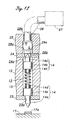
- a fifth embodiment as illustrated in Figure 12 is also possible.
- the parts corresponding to those of the previous embodiment are denoted with like numerals without repeating the description of such parts.
- the contact probe is provided with two moveable ends similarly as the embodiment of Figure 10, but the stem portion 14c is omitted from each conductive needle member 14.
- the holder comprises a main body consisting of a middle plate member 12, and an upper and lower plate member 23 and 24 integrally attached to an upper and lower surface of the middle plate member.
- the middle plate member 12 is formed with a straight hole serving as a main part of the support hole 13.
- the upper and lower plate members 23 and 24 are each provided with small diameter holes 23a and 24a, respective, both coaxially aligned with the main support hole 13.
- a compression coil spring 15 is received in the main support hole 13.
- Each conductive needle member 14 comprises a head 14a projecting out of the corresponding small diameter hole 23a, 24a, a large diameter portion 14b formed at the inner end of the head 14a, and a boss portion 14d extending from a rear end or inner end of the large diameter portion 14b and having a smaller diameter than the large diameter portion 14b.
- the conductive needle members 14 are each retained in the support hole by the annular shoulder defined between the main support hole 13 and the corresponding small diameter hole 23a, 24a engaging the annular shoulder defined on the outer end of the large diameter portion 14b.
- the head 14a of each conductive needle member 14 is slidably supported by the small diameter hole 23a, 23b provided in the corresponding one of the upper and lower plate members 23 and 24.
- a wiring plate 25 is placed over the upper surface of the upper plate member 24 at the top end of the holder as seen in the drawing, and is provided with a through hole 28 aligned coaxially with the holder hole 13.
- the through hole 28 includes a retaining hole 28a having a relatively large diameter and opposing the small diameter hole 24a, and a lead wire guide hole 28b having a relatively small diameter and facing away from the small diameter hole 24a.
- the retaining hole 28a receives a disk-shaped flattened portion 26a formed in an end portion of a lead wire 26 consisting of enameled wire or other single solid wire serving as a signal transmission line.
- This flattened portion 26a is formed by pressing an end portion of the lead wire 26 from a lateral direction or otherwise causing a plastic deformation, and is substantially formed into a disk shape defining a larger diameter than that of the lead wire 26 (the outer diameter of the enameled wire).
- the lead wire 26 is lead outward via the lead wire guide hole 28b having a relatively small diameter and extending through the wiring plate 25 from the retaining hole 28a in a continuous manner, and is connected to an external circuit 27 which may consist of a measuring instrument.
- the lead wire guide hole 28b is dimensioned so as to restrict the passage of the flattened portion 26a but allow the passage of the remaining part of the lead wire 26. Therefore, the flattened portion 26a received in the retaining hole 28a is prevented from being pulled out of the retaining hole 28a by being engaged by the shoulder defined between the retaining hole 28a and lead wire guide hole 28b.
- the axial end surface 26b of the lead wire 26 having the flattened portion 26a retained in the retaining hole 28a is located inside the retaining hole 28a so as to directly face the small diameter hole 24a, and allow the head 14a of the conductive needle member 14 to resiliently engage the end surface 26b of the lead wire 26.
- the head 14a of the conductive needle member 14 is subjected to a gold plating added with silver in a similar way as the previous embodiments. Because the head 14a is provided with a gold plate layer added with silver which is resistant to solder deposition, deposition of solder onto the head 14a can be avoided even after a repeated contacts with the objects to be tested.
- a sixth embodiment as illustrated in Figure 13 is also possible.
- the parts corresponding to those of the previous embodiment are denoted with like numerals without repeating the description of such parts.
- the contact probe head is provided with two moveable ends similarly as the embodiment of Figure 10, and the lower conductive needle member 14 as seen in the drawing is similar to that of Figure 6 while the upper conductive needle member 14 as seen in the drawing does away with the stem portion 14c.
- the holder for retaining the conductive needle members 14 and compression coil spring 15 in this case is formed by placing two plate members 12a and 12b one over the other similarly as the embodiment illustrated in Figure 6, and is provided with a support hole 13 passed across the thickness of the two mutually overlaid plate members 12a and 12b.
- the support hole 13 comprises small diameter holes 13a and 13b formed at the upper and lower surfaces, respectively, and given with a smaller diameter than the support hole 13.
- the two conductive needle members 14 are connected to the two ends of the compression coil spring 15 in a similar manner as those shown in Figure 6, but the upper closely wound section 15a corresponding the upper conductive needle member 14 is longer than the axial length of the boss portion 14b while the lower closely wound section 15b consists of a few turns of the coil wire so as to wrap around the corresponding boss portion 14d.
- the compression coil spring 15 and large diameter portions 14b of the two conductive needle members 14 are received in the support hole 13, and the conductive needle members 14 are each prevented from coming off by the large diameter portion 14b engaged by the shoulder defined between the support hole 13 and small diameter hole 13a, 13b.
- a relay board 16 On the upper surface of the upper plate member 12a as seen in the drawing is placed a relay board 16 forming signal exchanging means for relaying the electric signal similarly as the embodiment illustrated in Figure 6.
- the surface of an electric conductive path 16a formed in the relay board 16 facing the small diameter hole 13a is required to contact the pointed end of the head 14a of the conductive needle member 14, and is therefore formed flush with the lower surface (interface with respect to the base board element 12a) of the relay board 16 as seen in the drawing.
- the head 14a of the conductive needle member 14 is subjected to a gold plating added with silver in a similar way as the previous embodiments. Because the head 14a is provided with a gold plate layer added with silver which is resistant to solder deposition, deposition of solder onto the head 14a can be avoided even after repeated contacts with the objects to be tested.
- the silver content was 0.01% to 8% in the above described embodiments, but is more preferably 2% to 6% in the case of a conductive contact member in the form of a coil spring, and 0.5% to 2% in the case of a conductive contact member in the form of a needle member.
- Gold plating added with silver was performed to the conductive contact member in the foregoing embodiments, but other modes of surface processing are also possible. For instance, a rhodium plating process is also effective in reducing solder deposition onto the conductive contact member, and a similar advantage can be gained.
- the present invention in applications such as fixtures for testing semiconductor devices and circuit boards having solder balls or terminals having solder deposited thereon, and electric sockets for semiconductor device, transfer of solder from the object to be tested onto the conductive contact member can be reduced, and the number of possible contacts that can be effected before the cleaning of the solder deposition becomes necessary can be increased. Therefore, the run time of the test line can be increased, and the maintenance cost can be reduced.
Landscapes
- Physics & Mathematics (AREA)
- General Physics & Mathematics (AREA)
- Engineering & Computer Science (AREA)
- Microelectronics & Electronic Packaging (AREA)
- Measuring Leads Or Probes (AREA)
- Testing Of Individual Semiconductor Devices (AREA)
Abstract
Description
Claims (8)
- A conductive contact member for establishing an electric contact by being applied to an object to be contacted, comprising a layer of highly electrically conductive material resistant to solder deposition formed at least over a conductive contact part of said conductive contact member.
- A conductive contact member according to claim 1, wherein said layer is formed by plating.
- A conductive contact member according to claim 1, wherein said highly electrically conductive material essentially consists of gold added with silver.
- A conductive contact member according to claim 3, wherein silver is added to gold by 0.01% to 8%.
- A conductive contact member according to claim 1, wherein said conductive contact member is in the form of a member of group consisting of a coil, needle member having a pointed end, and rod member having a flat end.
- A conductive contact member according to claim 1, wherein said conductive contact member is made of steel.
- A conductive contact member according to claim 1, wherein said conductive contact member is in the form of a compression coil spring, and said solder resistant layer is formed around a coil wire forming said coil spring.
- A conductive contact member according to claim 1, wherein said conductive contact member is in the form of a compression coil spring having a contact part consisting of closely wound turns of a coil wire, and said solder resistant layer is formed over an outer surface of said closely wound turns of the coil wire.
Applications Claiming Priority (3)
| Application Number | Priority Date | Filing Date | Title |
|---|---|---|---|
| JP2000194511 | 2000-06-28 | ||
| JP2000194511 | 2000-06-28 | ||
| PCT/JP2001/005555 WO2002001232A1 (en) | 2000-06-28 | 2001-06-28 | Conductive contact |
Publications (3)
| Publication Number | Publication Date |
|---|---|
| EP1296145A1 true EP1296145A1 (en) | 2003-03-26 |
| EP1296145A4 EP1296145A4 (en) | 2005-07-20 |
| EP1296145B1 EP1296145B1 (en) | 2007-04-11 |
Family
ID=18693329
Family Applications (1)
| Application Number | Title | Priority Date | Filing Date |
|---|---|---|---|
| EP01943857A Expired - Lifetime EP1296145B1 (en) | 2000-06-28 | 2001-06-28 | Conductive contact |
Country Status (9)
| Country | Link |
|---|---|
| US (1) | US20030006787A1 (en) |
| EP (1) | EP1296145B1 (en) |
| JP (1) | JP4669651B2 (en) |
| KR (1) | KR100600092B1 (en) |
| CN (1) | CN1177227C (en) |
| AU (1) | AU6634901A (en) |
| DE (1) | DE60127837T2 (en) |
| TW (1) | TWI243244B (en) |
| WO (1) | WO2002001232A1 (en) |
Families Citing this family (20)
| Publication number | Priority date | Publication date | Assignee | Title |
|---|---|---|---|---|
| US6844749B2 (en) * | 2002-07-18 | 2005-01-18 | Aries Electronics, Inc. | Integrated circuit test probe |
| KR20040012318A (en) * | 2002-08-02 | 2004-02-11 | (주)티에스이 | Socket apparatus for testing a semiconductor device |
| US6846184B2 (en) * | 2003-01-24 | 2005-01-25 | High Connection Density Inc. | Low inductance electrical contacts and LGA connector system |
| US7201613B2 (en) * | 2003-03-18 | 2007-04-10 | Shin-Etsu Polymer Co., Ltd. | Pressure contact holding-type connector |
| KR100813095B1 (en) * | 2006-07-12 | 2008-03-17 | 주식회사 에이엠아이 씨 | Surface Mount Conductive Contact Terminals |
| WO2008072699A1 (en) * | 2006-12-15 | 2008-06-19 | Nhk Spring Co., Ltd. | Conductive contact holder, conductive contact unit and method for manufacturing conductive contact holder |
| US20100123476A1 (en) * | 2007-04-27 | 2010-05-20 | Nhk Spring Co., Ltd. | Conductive contact |
| JP2009288156A (en) * | 2008-05-30 | 2009-12-10 | Unitechno Inc | Inspection socket |
| JP4900843B2 (en) | 2008-12-26 | 2012-03-21 | 山一電機株式会社 | Electrical connection device for semiconductor device and contact used therefor |
| PH12012502538A1 (en) * | 2010-06-25 | 2013-02-11 | Nhk Spring Co Ltd | Contact probe and probe unit |
| CN104300251B (en) * | 2013-11-20 | 2017-09-22 | 中航光电科技股份有限公司 | Radio frequency connector between a kind of plate |
| EP3118940B1 (en) * | 2015-07-15 | 2018-06-06 | Siemens Aktiengesellschaft | Pin for a subsea connector |
| KR101707546B1 (en) * | 2016-12-15 | 2017-02-27 | 주식회사 에스알테크 | Interface probe pin |
| RU2724301C2 (en) * | 2018-12-17 | 2020-06-22 | Акционерное общество "НПО "Орион" | Method for increasing strength of multi-probe heads probes |
| CN110190430A (en) * | 2019-05-30 | 2019-08-30 | 深圳市力为电气有限公司 | A solderless connector |
| US11539167B2 (en) | 2020-09-17 | 2022-12-27 | Carlisle Interconnect Technologies, Inc. | Adjustable push on connector/adaptor |
| US11502440B2 (en) * | 2020-10-23 | 2022-11-15 | Carlisle Interconnect Technologies, Inc. | Multiport connector interface system |
| EP4080684B1 (en) * | 2021-04-20 | 2025-02-26 | Preci-Dip Sa | Piston assembly and spring-loaded contact |
| JP7182817B1 (en) | 2022-03-14 | 2022-12-05 | ユニコン株式会社 | Probe sheet and manufacturing method thereof |
| TWI899705B (en) * | 2023-11-20 | 2025-10-01 | 泰可廣科技股份有限公司 | Electrical connection components |
Family Cites Families (37)
| Publication number | Priority date | Publication date | Assignee | Title |
|---|---|---|---|---|
| NL126476C (en) * | 1962-08-07 | |||
| US3599326A (en) * | 1969-01-27 | 1971-08-17 | Philco Ford Corp | Method of forming electrical connections with solder resistant surfaces |
| US3864004A (en) * | 1972-11-30 | 1975-02-04 | Du Pont | Circuit board socket |
| US3989331A (en) * | 1974-08-21 | 1976-11-02 | Augat, Inc. | Dual-in-line socket |
| JPH0782028B2 (en) * | 1990-07-30 | 1995-09-06 | 日本発条株式会社 | Conductive contact |
| JPH0674970A (en) * | 1992-08-25 | 1994-03-18 | Takata Kk | Acceleration sensor |
| DE69405435T2 (en) * | 1993-03-16 | 1998-01-22 | Hewlett Packard Co | Method and device for the production of electrically interconnected circuits |
| JP2867209B2 (en) * | 1993-08-27 | 1999-03-08 | 日東電工株式会社 | Method of connecting flexible circuit board to contact object and structure thereof |
| JPH0719984U (en) * | 1993-09-17 | 1995-04-07 | 沖電線株式会社 | IC socket contact |
| US5500605A (en) * | 1993-09-17 | 1996-03-19 | At&T Corp. | Electrical test apparatus and method |
| JP3658029B2 (en) * | 1994-02-21 | 2005-06-08 | 株式会社ルネサステクノロジ | Connection apparatus and manufacturing method thereof |
| JP3246841B2 (en) * | 1994-03-31 | 2002-01-15 | 日東電工株式会社 | Probe structure |
| US5518964A (en) * | 1994-07-07 | 1996-05-21 | Tessera, Inc. | Microelectronic mounting with multiple lead deformation and bonding |
| JP3419110B2 (en) * | 1994-10-14 | 2003-06-23 | 株式会社神戸製鋼所 | Probe card |
| US6229320B1 (en) * | 1994-11-18 | 2001-05-08 | Fujitsu Limited | IC socket, a test method using the same and an IC socket mounting mechanism |
| JP2648120B2 (en) * | 1995-02-08 | 1997-08-27 | 山一電機株式会社 | Surface contact type connector |
| US5720098A (en) * | 1995-05-12 | 1998-02-24 | Probe Technology | Method for making a probe preserving a uniform stress distribution under deflection |
| US5791914A (en) * | 1995-11-21 | 1998-08-11 | Loranger International Corporation | Electrical socket with floating guide plate |
| US5931441A (en) * | 1996-02-29 | 1999-08-03 | Nikon Corporation | Method of isolating vibration in exposure apparatus |
| CN1255686C (en) * | 1996-04-12 | 2006-05-10 | 日本发条株式会社 | Conductive contact unit system |
| CH693478A5 (en) * | 1996-05-10 | 2003-08-15 | E Tec Ag | Contact socket for detachable connection of IC to PCB |
| US5928568A (en) * | 1996-06-24 | 1999-07-27 | Delco Electonics Corporation | Thick film circuit having conductor composition with coated metallic particles |
| JP3414593B2 (en) * | 1996-06-28 | 2003-06-09 | 日本発条株式会社 | Conductive contact |
| JPH09232057A (en) * | 1996-08-07 | 1997-09-05 | Enplas Corp | Ic socket |
| JP3458684B2 (en) * | 1997-11-28 | 2003-10-20 | 三菱マテリアル株式会社 | Contact probe |
| JP4060919B2 (en) * | 1997-11-28 | 2008-03-12 | 富士通株式会社 | Electrical connection device, contact manufacturing method, and semiconductor test method |
| JPH11204590A (en) * | 1998-01-14 | 1999-07-30 | Hitachi Ltd | Electrode plate and electrical inspection device for electronic components using the same |
| JP2000065892A (en) * | 1998-06-12 | 2000-03-03 | Machine Active Contact:Kk | Jig for continuity inspection |
| JP3196176B2 (en) * | 1998-08-24 | 2001-08-06 | 日本電子材料株式会社 | Method for manufacturing dissimilar metal bonded probe |
| JP2000276960A (en) * | 1999-03-29 | 2000-10-06 | Nec Corp | Combination electric contact, and relay and switch using it |
| US6442832B1 (en) * | 1999-04-26 | 2002-09-03 | Agilent Technologies, Inc. | Method for coupling a circuit board to a transmission line that includes a heat sensitive dielectric |
| US6352454B1 (en) * | 1999-10-20 | 2002-03-05 | Xerox Corporation | Wear-resistant spring contacts |
| US6341962B1 (en) * | 1999-10-29 | 2002-01-29 | Aries Electronics, Inc. | Solderless grid array connector |
| JP2002056911A (en) * | 2000-08-10 | 2002-02-22 | Yazaki Corp | Strip conductor connector |
| US6354872B1 (en) * | 2000-09-05 | 2002-03-12 | Avaya Technology Corp. | Cable connectors with modular shielding |
| JP2003133814A (en) * | 2001-10-24 | 2003-05-09 | Kyocera Corp | High frequency wiring board |
| KR20030069258A (en) * | 2002-02-19 | 2003-08-27 | 주식회사 휘라 포토닉스 | Digital signal cross-connection module |
-
2001
- 2001-06-28 JP JP2002506114A patent/JP4669651B2/en not_active Expired - Lifetime
- 2001-06-28 EP EP01943857A patent/EP1296145B1/en not_active Expired - Lifetime
- 2001-06-28 KR KR1020027002514A patent/KR100600092B1/en not_active Expired - Lifetime
- 2001-06-28 TW TW090116076A patent/TWI243244B/en not_active IP Right Cessation
- 2001-06-28 DE DE60127837T patent/DE60127837T2/en not_active Expired - Lifetime
- 2001-06-28 WO PCT/JP2001/005555 patent/WO2002001232A1/en not_active Ceased
- 2001-06-28 CN CNB018022111A patent/CN1177227C/en not_active Expired - Lifetime
- 2001-06-28 US US10/070,290 patent/US20030006787A1/en not_active Abandoned
- 2001-06-28 AU AU66349/01A patent/AU6634901A/en not_active Abandoned
Also Published As
| Publication number | Publication date |
|---|---|
| DE60127837D1 (en) | 2007-05-24 |
| JP4669651B2 (en) | 2011-04-13 |
| CN1386197A (en) | 2002-12-18 |
| AU6634901A (en) | 2002-01-08 |
| EP1296145A4 (en) | 2005-07-20 |
| CN1177227C (en) | 2004-11-24 |
| US20030006787A1 (en) | 2003-01-09 |
| KR20020054316A (en) | 2002-07-06 |
| DE60127837T2 (en) | 2007-09-06 |
| TWI243244B (en) | 2005-11-11 |
| EP1296145B1 (en) | 2007-04-11 |
| WO2002001232A1 (en) | 2002-01-03 |
| KR100600092B1 (en) | 2006-07-13 |
Similar Documents
| Publication | Publication Date | Title |
|---|---|---|
| EP1296145B1 (en) | Conductive contact | |
| US7091734B2 (en) | Electroconductive contact unit | |
| US7081767B2 (en) | Electroconductive contact unit | |
| JP3326095B2 (en) | Conductive contact | |
| US6150616A (en) | Electroconductive contact unit system | |
| US6873168B2 (en) | Conductive coil contact member | |
| KR100745104B1 (en) | Combination of contactor probes, electrical probe units, probe assemblies and insulators for contactor probes and elastic conductive probe assemblies for contactor probes | |
| US6900651B1 (en) | Electroconductive contact unit assembly | |
| JPWO2002001232A1 (en) | Conductive Contact | |
| WO2000031828A2 (en) | Electrical contact system | |
| KR20140013985A (en) | Jig and probe for inspection | |
| JP2012122905A (en) | Contact probe | |
| JP4167202B2 (en) | Conductive contact | |
| KR200182523Y1 (en) | Probing device | |
| KR20250149004A (en) | Testing probe and test socket having the same | |
| JPWO2000003251A1 (en) | Conductive Contact |
Legal Events
| Date | Code | Title | Description |
|---|---|---|---|
| PUAI | Public reference made under article 153(3) epc to a published international application that has entered the european phase |
Free format text: ORIGINAL CODE: 0009012 |
|
| 17P | Request for examination filed |
Effective date: 20020510 |
|
| AK | Designated contracting states |
Kind code of ref document: A1 Designated state(s): AT BE CH CY DE DK ES FI FR GB GR IE IT LI LU MC NL PT SE TR |
|
| AX | Request for extension of the european patent |
Extension state: AL LT LV MK RO SI |
|
| RBV | Designated contracting states (corrected) |
Designated state(s): AT BE CH DE FR IT LI |
|
| A4 | Supplementary search report drawn up and despatched |
Effective date: 20050603 |
|
| GRAP | Despatch of communication of intention to grant a patent |
Free format text: ORIGINAL CODE: EPIDOSNIGR1 |
|
| DAX | Request for extension of the european patent (deleted) | ||
| RBV | Designated contracting states (corrected) |
Designated state(s): DE FR IT |
|
| DAX | Request for extension of the european patent (deleted) | ||
| RBV | Designated contracting states (corrected) |
Designated state(s): DE FR IT |
|
| RBV | Designated contracting states (corrected) |
Designated state(s): DE FR IT |
|
| GRAS | Grant fee paid |
Free format text: ORIGINAL CODE: EPIDOSNIGR3 |
|
| GRAA | (expected) grant |
Free format text: ORIGINAL CODE: 0009210 |
|
| AK | Designated contracting states |
Kind code of ref document: B1 Designated state(s): DE FR IT |
|
| REF | Corresponds to: |
Ref document number: 60127837 Country of ref document: DE Date of ref document: 20070524 Kind code of ref document: P |
|
| ET | Fr: translation filed | ||
| PLBE | No opposition filed within time limit |
Free format text: ORIGINAL CODE: 0009261 |
|
| STAA | Information on the status of an ep patent application or granted ep patent |
Free format text: STATUS: NO OPPOSITION FILED WITHIN TIME LIMIT |
|
| 26N | No opposition filed |
Effective date: 20080114 |
|
| PGFP | Annual fee paid to national office [announced via postgrant information from national office to epo] |
Ref country code: FR Payment date: 20110621 Year of fee payment: 11 |
|
| PGFP | Annual fee paid to national office [announced via postgrant information from national office to epo] |
Ref country code: IT Payment date: 20110623 Year of fee payment: 11 |
|
| PG25 | Lapsed in a contracting state [announced via postgrant information from national office to epo] |
Ref country code: IT Free format text: LAPSE BECAUSE OF NON-PAYMENT OF DUE FEES Effective date: 20120628 |
|
| REG | Reference to a national code |
Ref country code: FR Ref legal event code: ST Effective date: 20130228 |
|
| PG25 | Lapsed in a contracting state [announced via postgrant information from national office to epo] |
Ref country code: FR Free format text: LAPSE BECAUSE OF NON-PAYMENT OF DUE FEES Effective date: 20120702 |
|
| PGFP | Annual fee paid to national office [announced via postgrant information from national office to epo] |
Ref country code: DE Payment date: 20200617 Year of fee payment: 20 |
|
| REG | Reference to a national code |
Ref country code: DE Ref legal event code: R071 Ref document number: 60127837 Country of ref document: DE |