EP1294183A1 - Méthode de fabrication d'une caméra integré et dispositif d'illumination - Google Patents
Méthode de fabrication d'une caméra integré et dispositif d'illumination Download PDFInfo
- Publication number
- EP1294183A1 EP1294183A1 EP02254206A EP02254206A EP1294183A1 EP 1294183 A1 EP1294183 A1 EP 1294183A1 EP 02254206 A EP02254206 A EP 02254206A EP 02254206 A EP02254206 A EP 02254206A EP 1294183 A1 EP1294183 A1 EP 1294183A1
- Authority
- EP
- European Patent Office
- Prior art keywords
- mould
- encapsulant
- cmos sensor
- camera
- lens unit
- Prior art date
- Legal status (The legal status is an assumption and is not a legal conclusion. Google has not performed a legal analysis and makes no representation as to the accuracy of the status listed.)
- Withdrawn
Links
Images


Classifications
-
- H—ELECTRICITY
- H04—ELECTRIC COMMUNICATION TECHNIQUE
- H04N—PICTORIAL COMMUNICATION, e.g. TELEVISION
- H04N23/00—Cameras or camera modules comprising electronic image sensors; Control thereof
- H04N23/50—Constructional details
- H04N23/51—Housings
-
- H—ELECTRICITY
- H04—ELECTRIC COMMUNICATION TECHNIQUE
- H04N—PICTORIAL COMMUNICATION, e.g. TELEVISION
- H04N23/00—Cameras or camera modules comprising electronic image sensors; Control thereof
- H04N23/56—Cameras or camera modules comprising electronic image sensors; Control thereof provided with illuminating means
-
- H—ELECTRICITY
- H04—ELECTRIC COMMUNICATION TECHNIQUE
- H04N—PICTORIAL COMMUNICATION, e.g. TELEVISION
- H04N23/00—Cameras or camera modules comprising electronic image sensors; Control thereof
- H04N23/50—Constructional details
- H04N23/555—Constructional details for picking-up images in sites, inaccessible due to their dimensions or hazardous conditions, e.g. endoscopes or borescopes
Definitions
- the present application relates to a method of manufacture of an integrated camera and lighting device.
- CMOS sensors have a disadvantage in that they are not very resistant to heat. Indeed, there is only a relatively small temperature range in which a CMOS sensor will provide a good signal.
- the present invention provides a method of manufacture of an integrated camera and illumination device comprising:
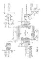
- circuit board 10 upon the back of which is mounted an electronic circuit and on the front of which is mounted a CMOS sensor 12.
- the sensor 12 is first cleaned with a lens tissue and then a neoprene gasket 13 with a central aperture 14 is fixed overlaying the CMOS sensor 12 so that the aperture 14 lines up with the image area on the CMOS sensor 12.
- Figure 1a there can also be seen a metal sleeve 15 which is used to cover the printed circuit board 10. Also, a lens assembly 16 is shown which fixed in place in front of the CMOS sensor 12 and abutting and sealing with the neoprene gasket 13.
- FIG 1a there can further be seen twelve LEDs 17.
- the printed circuit on which the LEDs 17 are mounted is soldered to underlying contacts 11 on the front of the circuit board 10. Also a lens cover 18 is fixed in place at the front of lens assembly 16.
- the assembly 34 shown in Figure 1b results from assembly of the components of Figure 1a.
- the assembly 34 is then inserted in an outer metal case 31 which has slots 32 provided on an inner surface.
- the assembly 34 and the case 31 are then placed together in a mould.
- the mould will be specially constructed with a rubber element at one end shaped to press against the front curved surfaces of the LEDs 17 and also the front cover 18 at the front of the lens assembly 16.
- an encapsulant in a liquid state is introduced into the mould from the rear of the apparatus, i.e. from the back of the circuit board 10.
- the encapsulant compound flows through the mould through the slots 32 provided on the interior surface of the metallic case 31.
- the encapsulant surrounds the printed circuit board 10 and the lens assembly 16, but the sealing of the bottom of the lens assembly 16 on the neoprene washer 13 and the sealing of the lens cover 18 on the rubber surface of the mould prevent ingress of the encapsulant into the lens assembly 16 and therefore prevents the CMOS sensor 12 being covered.
- the encapsulant will flow around the LEDs 17, but because the surrounded ends of LEDs 17 abut against the rubber inner surface at the end of the mould the ends of the LEDs 17 are not covered by the encapsulant. Therefore, after the encapsulant is cured and sets hard the resulting component has LEDs 17 which have exposed ends and also a lens assembly which is not covered by the encapsulant. However, all of the components are secured in position by the solidified encapsulant.
- the encapsulated integrated camera and lighting device 35 is shown in Figure 1c.
- an LED 17 can be seen surrounded by the encapsulant 19. However, it can be seen that the front of the LED 17 is exposed through an aperture 20 defined in the encapsulant. This will be defined by a rubber projection in the mould interior which engages with the front of the LED 17 when the component is assembled into the mould and covers the front of the LED 17 when the encapsulant is introduced.
- the encapsulant used in the preferred embodiment is STYCAST 2850 FT(RTM) .
- This is a two-component epoxy encapsulant. It has excellent electrical grade insulation properties and excellent resistance to chemicals and solvents.
- the encapsulant is chosen because it has unusually high thermal conductivity and low thermal expansion. Thus, the encapsulant provides good electrical insulation and protects the electronic components of the integrated camera and lighting apparatus whilst also being able to transfer heat away from the components to the exterior.
- the encapsulant is supplied in Europe by Emerson & Cuming who have an office at Nijverheidstraat, 7, B2260, Westerlo, Belgium.
- the CMOS sensor 12 will be of a standard type, e.g. supplied by Omnivision (RTM), for instance as used for webcams.
- RTM Omnivision
- FIG. 2a and Figure 2b the encapsulated integrated camera and illumination device can be seen.
- the front elevation view shows the plurality of LEDs 17 visible at the front of the apparatus in a circle surrounding the CMOS sensor 12. Also, the uncovered lens screen 18 can be seen.
- the circuit board 10 has a circuit 11 of electronic components provided on its reverse and a CMOS sensor 12 provided on the front. There is shown the neoprene washer 13 which seals against the lens assembly 16. The electrical contact 20 for an LED 17 is also shown in the Figure. It will be appreciated that all of the electrical components of the circuit board 11 are encapsulated in the manner previously described.
- the device illustrated in Figure 2a and Figure 2b comprises a combination of camera apparatus and illumination apparatus all encapsulated together in an integral unit.
- the device can be used in many applications. In one such application, the device is used at the end of a flexible rod and the rod is used to force the device down a pipe.
- the camera and lighting device 21 is shown attached to a cable 22 by a hose assembly 23.
- the hose assembly comprises a flexible elastomeric tube 24 surrounded by a spring 25 which together form a flexible arrangement whereby the camera can be pushed down curved pipes.
- the camera and lighting device described above is very compact in nature having an overall diameter of 25 mm, as compared with a diameter of 32 mm which was common previously. This enables the device to be used in small diameter pipes.
- the device is very robust and resilient nevertheless, because of the encapsulated nature of the assembly described above.
- CMOS sensors provide ideal camera elements for video inspection systems such as that of the present invention, they are difficult to use because they must be maintained within a specified temperature range. Usually this would require the use of a larger area to dissipate the heat produced in the regulator circuits and hence a larger camera.
- the present invention uses the lighting circuit as a pre-regulator for the camera circuit. This ensures that the heat dissipated in the camera circuit is kept to a minimum.
- Figure 4 shows an arrangement of twelve LED's wired as three strings of four LED's 17. The current through these strings is regulated by the sub-circuit consisting of a bipolar transistor 26, constant-current diode 27, and the resistors 27b, 27c and 27d. This arrangement provides a constant voltage across the resistor 27d due to the constant current through the base-emitter junction of the transistor 26.
- FIG. 5 the figure shows the circuit diagram for the printed circuit board of the sensor.
- the sensor obtains its power from the illumination assembly via the line "Camera Power Return".
- This is the output rail P2 shown in Figure 4.
- the rail P2 supplies a constant current.
- the current is shared between the two active components shown in Figure 5, these being IC1 which is an integrated circuit which acts as a voltage regulator and the integrated circuit IC3, which is the CMOS sensor 12.
- the constant current source is set to 44 milliamps and most of this current is demanded by IC3, the CMOS sensor 12.
- the minimum current demand of this sensor is 25 milliamps. Any excess current is dissipated in the component IC1 which has a maximum value of 14 milliamps with a dissipation value of 70 milliwatts, the device having a maximum rating of 330 milliwatts.
- the 5-volt output shown in the part of the circuit diagram which includes IC1 is used as the 5-volt input for the other parts of the circuit diagram.
- IC4 is an integrated circuit which is used to set the "white balance" for the sensor 12.
- colour temperature For the purposes of sensors such as the sensor 12 colours are referred to by "colour temperature”.
- the circuit IC4 is used to set the colour temperature of white as sensed by the CMOS sensor 12 at 6,500K. This technique is well known and will not be described in detail here.
- the circuit IC4 operates only on power-up of the apparatus and is then dormant afterwards, demanding less than a milliamp of current.
- the output of the CMOS sensor 12 is provided at P7 after amplification by an Operational Amplifier 30 and also a reference signal is provided at P8. These signals are then used to provide a video output in a known manner.
- the apparatus of the present invention provides a very compact integrated camera and illumination device by using LEDs and constructing the circuit driving the LEDs in such a way that the circuit provides a constant current output, this constant current output then being used by the CMOS sensor so that the temperature of the CMOS sensor is always kept in an acceptable range.
- the functioning of the overall device is improved by the encapsulation of the components in an encapsulant which is a good conductor of heat so that all heat generated by the circuits shown in Figures 4 and 5 can be dissipated via the encapsulant to the exterior of the device.
- the resulting device is also very robust and the circuitry well protected.
- zone zero environment Whilst the embodiment described above is suitable for the majority of applications, there is defined for video inspection apparatus a zone zero environment and video inspection apparatus must be able to meet the guidelines laid down for zone zero operation if it is to be used in such environments.
- An example would be a recently-emptied fuel tank which would usually be full of fuel vapour. A very low power spark could ignite the vapour and cause an explosion. Therefore, any camera and illumination device used must be very low power in order to avoid the possibility of the power passing through the equipment being sufficient to generate a spark.
- a second embodiment of camera and illumination device which can operate in zone zero conditions will now be described. It is identical to the first embodiment save for modified circuitry.
- the modified circuitry is shown in Figures 6 and 7. Contrasting Figure 6 with Figure 4 the significant difference is that there are four strings of three LEDs 17 rather than three strings of four LEDs 17. The reason for this is that the voltage across the LEDs 17 can be reduced. Apart from this difference, the circuitry and its functioning remains the same.
- the circuit is designed so that there can be two concurrent component failures (open or closed circuit) without increasing the current output on the rail P2 above 55 milliamps. As before, the current supplied via all four strings of LEDs 17 is used to power the circuit of the CMOS sensor 12.
- Circuitry of the CMOS sensor 12 is shown in Figure 7. In the main this is identical to the circuitry shown in Figure 5. A significant difference is that the output of the CMOS sensor 12 is not amplified. The output of the CMOS sensor 12 is not amplified within the integrated camera and illumination apparatus itself, but instead is relayed on unamplified to the output of the apparatus for amplification later on (outside of the dangerous environment). A second significant difference is that the capacitance values of many of the capacitors (eg C14, C12, C13, C1, C7, C5) have been reduced by more than an order of magnitude. This is required so that in the event of a fault such as the connecting cables being severed then the camera apparatus does not become a voltage source due to electrical energy stored within the internal capacitance.
- the capacitance values of many of the capacitors eg C14, C12, C13, C1, C7, C5
- the assembly shown is inherently safe.
- the worst-case fault mode foresees that all capacitors and the internal capacitance of the integrated circuits is put in parallel and joined across the supply and output rails.
- the voltage supplied to the camera circuit is 21 volts.
- the capacitance allowed by the relevant British Standard BS EN 50020 is 188 nF.
- All the discrete capacitors are rated at a worst-case of 10% tolerance.
- the total capacitance of the circuit is 169.882 nF. With the 10% tolerance, the total is 186.9 nF.
- the capacitance of the two integrated circuits are somewhere between 2 pF and 2.5 pF at 5 volts up to 3.2 pF at 2.25 volts.
- the CMOS sensor is a 48-pin device and assuming the worst case where one pin is connected to the negative rail and the remaining 47 are connected to the positive rail, there will be a parallel capacitance of 150.4 pF.
- the same calculation can be made with the integrated circuit IC4 with one leg grounded and the other seven connected to the positive rail giving a total of 22.4 pF.
- the overall capacitance of the circuit is therefore a maximum of 187.07 nanofarads and this is within the required range.
- the supply voltage of the apparatus and hence the internal capacitance may change but the configuration will remain the same.
- any resin or resin mixture would be suitable, e.g. epoxy resin, polyester resin or other thermosetting polymers, provided that the resin does not need to be cured at a temperature elevated to such a degree that the electronic arrangements would be damaged.
- the resin would be introduced in liquid state into the mould and then cured. It is also possible to use thermoplastics, introducing them into the mould at an elevated temperature in a liquid state and then allowing them to cool and solidify.
Applications Claiming Priority (2)
| Application Number | Priority Date | Filing Date | Title |
|---|---|---|---|
| GB0119360 | 2001-08-08 | ||
| GB0119360A GB2378522B (en) | 2001-08-08 | 2001-08-08 | Integrated camera and lighting device and a method of manufacture thereof |
Publications (1)
| Publication Number | Publication Date |
|---|---|
| EP1294183A1 true EP1294183A1 (fr) | 2003-03-19 |
Family
ID=9920040
Family Applications (2)
| Application Number | Title | Priority Date | Filing Date |
|---|---|---|---|
| EP02254204A Expired - Lifetime EP1292127B1 (fr) | 2001-08-08 | 2002-06-17 | Caméra integrée et dispositif d'illumination |
| EP02254206A Withdrawn EP1294183A1 (fr) | 2001-08-08 | 2002-06-17 | Méthode de fabrication d'une caméra integré et dispositif d'illumination |
Family Applications Before (1)
| Application Number | Title | Priority Date | Filing Date |
|---|---|---|---|
| EP02254204A Expired - Lifetime EP1292127B1 (fr) | 2001-08-08 | 2002-06-17 | Caméra integrée et dispositif d'illumination |
Country Status (5)
| Country | Link |
|---|---|
| US (1) | US6752951B2 (fr) |
| EP (2) | EP1292127B1 (fr) |
| AT (1) | ATE500689T1 (fr) |
| DE (1) | DE60239313D1 (fr) |
| GB (2) | GB2378522B (fr) |
Cited By (1)
| Publication number | Priority date | Publication date | Assignee | Title |
|---|---|---|---|---|
| WO2010103426A1 (fr) * | 2009-03-12 | 2010-09-16 | T. & A. S.A. - Tecnologie E Ambiente | Dispositif d'inspection vidéo pour des zones à atmosphères potentiellement explosives |
Families Citing this family (9)
| Publication number | Priority date | Publication date | Assignee | Title |
|---|---|---|---|---|
| US6831679B1 (en) * | 2000-02-17 | 2004-12-14 | Deepsea Power & Light Company | Video camera head with thermal feedback lighting control |
| WO2005065526A1 (fr) * | 2004-01-07 | 2005-07-21 | Olympus Corporation | Dispositif medical de type capsule, enceinte de capsule medicale et procede pour les produire |
| JP4598498B2 (ja) * | 2004-11-29 | 2010-12-15 | オリンパス株式会社 | 被検体内導入装置 |
| DE102005020138B4 (de) * | 2005-04-29 | 2007-03-08 | Siemens Ag | Optisches Modul mit integrierter Lichtquelle |
| GB2433877A (en) * | 2005-12-20 | 2007-07-11 | Glyn Howard | Remote inspection camera |
| US20090027497A1 (en) | 2007-07-26 | 2009-01-29 | Stephen Thomas Peacock | Camera light |
| KR101271730B1 (ko) | 2007-08-29 | 2013-06-04 | 삼성테크윈 주식회사 | 감시카메라 |
| US8200074B1 (en) * | 2010-02-05 | 2012-06-12 | Paige Melancon | Apparatus for murky water camera inspection of under-water construction features |
| JP6324159B2 (ja) * | 2014-03-28 | 2018-05-16 | オリンパス株式会社 | カプセル内視鏡 |
Citations (3)
| Publication number | Priority date | Publication date | Assignee | Title |
|---|---|---|---|---|
| US5089895A (en) * | 1990-05-07 | 1992-02-18 | Cues, Inc. | Encapsulated television camera and method and apparatus for fabricating same |
| FR2775151A1 (fr) * | 1998-02-17 | 1999-08-20 | Renault | Dispositif de visualisation par camera a tete flexible |
| EP0941691A1 (fr) * | 1998-03-11 | 1999-09-15 | Welch Allyn, Inc. | Système d'imagerie vidéo de construction compacte |
Family Cites Families (12)
| Publication number | Priority date | Publication date | Assignee | Title |
|---|---|---|---|---|
| US4651558A (en) * | 1985-09-13 | 1987-03-24 | Cues, Inc. | Method and apparatus for inspecting lateral lines |
| FR2625010B1 (fr) * | 1987-12-18 | 1990-04-27 | Sodern | Illuminateur de forte puissance pour camera |
| US4923908A (en) * | 1988-10-14 | 1990-05-08 | Zenith Electronics Corporation | Epoxy compositions, and method of making same |
| US4882600A (en) * | 1989-04-07 | 1989-11-21 | Eastman Kodak Company | Underwater disposable single-use camera |
| US5239412A (en) * | 1990-02-05 | 1993-08-24 | Sharp Kabushiki Kaisha | Solid image pickup device having microlenses |
| US5287133A (en) * | 1991-11-27 | 1994-02-15 | Bohley's Diving Service, Inc. | Self-orienting pipe inspection apparatus and method |
| JP2791216B2 (ja) * | 1992-07-17 | 1998-08-27 | ヴィエルティー コーポレーション | 電気部品用パッケージ、電力損発生部品の取付方法、及び導体端子ピンと回路基板との接続方法 |
| US5691766A (en) * | 1992-09-04 | 1997-11-25 | Canon Kabushiki Kaisha | Video camera with vented light |
| JP2000111808A (ja) * | 1998-10-02 | 2000-04-21 | Kubota Corp | 管内検査装置 |
| US6734893B1 (en) * | 1998-12-04 | 2004-05-11 | Olympus Winter & Ibe Gmbh | Endoscopy illumination system for stroboscopy |
| JP4477168B2 (ja) * | 1999-09-06 | 2010-06-09 | オリンパス株式会社 | 電子内視鏡 |
| US6545716B2 (en) * | 2001-09-13 | 2003-04-08 | Tracey Gardiner | Camera body for protecting components |
-
2001
- 2001-08-08 GB GB0119360A patent/GB2378522B/en not_active Expired - Fee Related
-
2002
- 2002-02-11 GB GB0203187A patent/GB2378523B/en not_active Expired - Fee Related
- 2002-06-17 AT AT02254204T patent/ATE500689T1/de not_active IP Right Cessation
- 2002-06-17 DE DE60239313T patent/DE60239313D1/de not_active Expired - Lifetime
- 2002-06-17 EP EP02254204A patent/EP1292127B1/fr not_active Expired - Lifetime
- 2002-06-17 EP EP02254206A patent/EP1294183A1/fr not_active Withdrawn
- 2002-08-07 US US10/212,791 patent/US6752951B2/en not_active Expired - Fee Related
Patent Citations (3)
| Publication number | Priority date | Publication date | Assignee | Title |
|---|---|---|---|---|
| US5089895A (en) * | 1990-05-07 | 1992-02-18 | Cues, Inc. | Encapsulated television camera and method and apparatus for fabricating same |
| FR2775151A1 (fr) * | 1998-02-17 | 1999-08-20 | Renault | Dispositif de visualisation par camera a tete flexible |
| EP0941691A1 (fr) * | 1998-03-11 | 1999-09-15 | Welch Allyn, Inc. | Système d'imagerie vidéo de construction compacte |
Cited By (1)
| Publication number | Priority date | Publication date | Assignee | Title |
|---|---|---|---|---|
| WO2010103426A1 (fr) * | 2009-03-12 | 2010-09-16 | T. & A. S.A. - Tecnologie E Ambiente | Dispositif d'inspection vidéo pour des zones à atmosphères potentiellement explosives |
Also Published As
| Publication number | Publication date |
|---|---|
| GB2378523A (en) | 2003-02-12 |
| EP1292127A1 (fr) | 2003-03-12 |
| US6752951B2 (en) | 2004-06-22 |
| GB0203187D0 (en) | 2002-03-27 |
| US20030030180A1 (en) | 2003-02-13 |
| DE60239313D1 (de) | 2011-04-14 |
| ATE500689T1 (de) | 2011-03-15 |
| EP1292127B1 (fr) | 2011-03-02 |
| GB0119360D0 (en) | 2001-10-03 |
| GB2378523B (en) | 2003-07-16 |
| GB2378522B (en) | 2003-08-13 |
| GB2378522A (en) | 2003-02-12 |
Similar Documents
| Publication | Publication Date | Title |
|---|---|---|
| US6741286B2 (en) | Integrated camera and illumination device having a regulated current | |
| US6752951B2 (en) | Method of manufacture of an integrated camera and lighting device | |
| US7665861B2 (en) | Led module for illumination systems | |
| US9052092B2 (en) | Sealed pixel assemblies, kits and methods | |
| US5554049A (en) | Inline indicating interconnect | |
| US8075152B2 (en) | Hermetic light-emitting device | |
| US20090021497A1 (en) | Flexible pixel element and signal distribution means | |
| US8743207B2 (en) | Infrared camera architecture systems and methods | |
| FR2822326B1 (fr) | Camera electronique a faible cout en technologie des circuits integres | |
| US20180187878A1 (en) | Lighting Device, LED Module for a Lighting Device, and Method for Assembling a Lighting Device | |
| CN103890653B (zh) | 冷却的航空相机 | |
| US20100013922A1 (en) | Surveillance camera | |
| KR20130012861A (ko) | 카메라 모듈의 케이블 연결구조 | |
| US7834564B2 (en) | Actuating device for motor vehicle components | |
| JP5602107B2 (ja) | 撮像装置 | |
| KR200398252Y1 (ko) | Cctv용 카메라 | |
| KR102337971B1 (ko) | 투명필름 엘이디 디스플레이에서 커넥터 빠짐에 의한 에러를 방지하는 보조장치 | |
| US20190377244A1 (en) | Dashboard camera | |
| JP2003230031A5 (fr) | ||
| CN212411304U (zh) | 基于全波段光谱的快速扫码装置 | |
| CN113219293B (zh) | 光学附件检测电路及照明设备 | |
| US10465891B2 (en) | Circuit board and lighting apparatus | |
| JPH02213165A (ja) | 固体撮像装置 | |
| JP7481801B2 (ja) | 信号発生器のデジタル入力信号を受信するためのデジタル入力回路 | |
| JP2002345167A (ja) | 非常用照明装置 |
Legal Events
| Date | Code | Title | Description |
|---|---|---|---|
| PUAI | Public reference made under article 153(3) epc to a published international application that has entered the european phase |
Free format text: ORIGINAL CODE: 0009012 |
|
| AK | Designated contracting states |
Kind code of ref document: A1 Designated state(s): AT BE CH CY DE DK ES FI FR GB GR IE IT LI LU MC NL PT SE TR Designated state(s): AT BE CH CY DE DK ES FI FR GB GR IE IT LI LU MC NL PT SE TR |
|
| AX | Request for extension of the european patent |
Extension state: AL LT LV MK RO SI |
|
| 17P | Request for examination filed |
Effective date: 20030918 |
|
| AKX | Designation fees paid |
Designated state(s): AT BE CH CY DE DK ES FI FR GB GR IE IT LI LU MC NL PT SE TR |
|
| RAP1 | Party data changed (applicant data changed or rights of an application transferred) |
Owner name: RADIODETECTION LIMITED |
|
| STAA | Information on the status of an ep patent application or granted ep patent |
Free format text: STATUS: THE APPLICATION HAS BEEN WITHDRAWN |
|
| 18W | Application withdrawn |
Effective date: 20050525 |