EP1290735B1 - Halbleiterbauelement - Google Patents
Halbleiterbauelement Download PDFInfo
- Publication number
- EP1290735B1 EP1290735B1 EP01938146A EP01938146A EP1290735B1 EP 1290735 B1 EP1290735 B1 EP 1290735B1 EP 01938146 A EP01938146 A EP 01938146A EP 01938146 A EP01938146 A EP 01938146A EP 1290735 B1 EP1290735 B1 EP 1290735B1
- Authority
- EP
- European Patent Office
- Prior art keywords
- region
- trench
- drain
- source
- semiconductor device
- Prior art date
- Legal status (The legal status is an assumption and is not a legal conclusion. Google has not performed a legal analysis and makes no representation as to the accuracy of the status listed.)
- Expired - Lifetime
Links
Images



Classifications
-
- H—ELECTRICITY
- H10—SEMICONDUCTOR DEVICES; ELECTRIC SOLID-STATE DEVICES NOT OTHERWISE PROVIDED FOR
- H10D—INORGANIC ELECTRIC SEMICONDUCTOR DEVICES
- H10D30/00—Field-effect transistors [FET]
- H10D30/60—Insulated-gate field-effect transistors [IGFET]
- H10D30/601—Insulated-gate field-effect transistors [IGFET] having lightly-doped drain or source extensions, e.g. LDD IGFETs or DDD IGFETs
- H10D30/603—Insulated-gate field-effect transistors [IGFET] having lightly-doped drain or source extensions, e.g. LDD IGFETs or DDD IGFETs having asymmetry in the channel direction, e.g. lateral high-voltage MISFETs having drain offset region or extended drain IGFETs [EDMOS]
-
- H—ELECTRICITY
- H10—SEMICONDUCTOR DEVICES; ELECTRIC SOLID-STATE DEVICES NOT OTHERWISE PROVIDED FOR
- H10D—INORGANIC ELECTRIC SEMICONDUCTOR DEVICES
- H10D30/00—Field-effect transistors [FET]
- H10D30/60—Insulated-gate field-effect transistors [IGFET]
- H10D30/601—Insulated-gate field-effect transistors [IGFET] having lightly-doped drain or source extensions, e.g. LDD IGFETs or DDD IGFETs
- H10D30/608—Insulated-gate field-effect transistors [IGFET] having lightly-doped drain or source extensions, e.g. LDD IGFETs or DDD IGFETs having non-planar bodies, e.g. having recessed gate electrodes
-
- H—ELECTRICITY
- H10—SEMICONDUCTOR DEVICES; ELECTRIC SOLID-STATE DEVICES NOT OTHERWISE PROVIDED FOR
- H10D—INORGANIC ELECTRIC SEMICONDUCTOR DEVICES
- H10D64/00—Electrodes of devices having potential barriers
- H10D64/20—Electrodes characterised by their shapes, relative sizes or dispositions
- H10D64/27—Electrodes not carrying the current to be rectified, amplified, oscillated or switched, e.g. gates
- H10D64/311—Gate electrodes for field-effect devices
- H10D64/411—Gate electrodes for field-effect devices for FETs
- H10D64/511—Gate electrodes for field-effect devices for FETs for IGFETs
- H10D64/512—Disposition of the gate electrodes, e.g. buried gates
- H10D64/513—Disposition of the gate electrodes, e.g. buried gates within recesses in the substrate, e.g. trench gates, groove gates or buried gates
-
- H—ELECTRICITY
- H10—SEMICONDUCTOR DEVICES; ELECTRIC SOLID-STATE DEVICES NOT OTHERWISE PROVIDED FOR
- H10D—INORGANIC ELECTRIC SEMICONDUCTOR DEVICES
- H10D12/00—Bipolar devices controlled by the field effect, e.g. insulated-gate bipolar transistors [IGBT]
- H10D12/411—Insulated-gate bipolar transistors [IGBT]
- H10D12/441—Vertical IGBTs
- H10D12/461—Vertical IGBTs having non-planar surfaces, e.g. having trenches, recesses or pillars in the surfaces of the emitter, base or collector regions
- H10D12/481—Vertical IGBTs having non-planar surfaces, e.g. having trenches, recesses or pillars in the surfaces of the emitter, base or collector regions having gate structures on slanted surfaces, on vertical surfaces, or in grooves, e.g. trench gate IGBTs
-
- H—ELECTRICITY
- H10—SEMICONDUCTOR DEVICES; ELECTRIC SOLID-STATE DEVICES NOT OTHERWISE PROVIDED FOR
- H10D—INORGANIC ELECTRIC SEMICONDUCTOR DEVICES
- H10D30/00—Field-effect transistors [FET]
- H10D30/80—FETs having rectifying junction gate electrodes
- H10D30/87—FETs having Schottky gate electrodes, e.g. metal-semiconductor FETs [MESFET]
- H10D30/877—FETs having Schottky gate electrodes, e.g. metal-semiconductor FETs [MESFET] having recessed gate electrodes
-
- H—ELECTRICITY
- H10—SEMICONDUCTOR DEVICES; ELECTRIC SOLID-STATE DEVICES NOT OTHERWISE PROVIDED FOR
- H10D—INORGANIC ELECTRIC SEMICONDUCTOR DEVICES
- H10D62/00—Semiconductor bodies, or regions thereof, of devices having potential barriers
- H10D62/10—Shapes, relative sizes or dispositions of the regions of the semiconductor bodies; Shapes of the semiconductor bodies
- H10D62/124—Shapes, relative sizes or dispositions of the regions of semiconductor bodies or of junctions between the regions
- H10D62/126—Top-view geometrical layouts of the regions or the junctions
- H10D62/127—Top-view geometrical layouts of the regions or the junctions of cellular field-effect devices, e.g. multicellular DMOS transistors or IGBTs
-
- H—ELECTRICITY
- H10—SEMICONDUCTOR DEVICES; ELECTRIC SOLID-STATE DEVICES NOT OTHERWISE PROVIDED FOR
- H10D—INORGANIC ELECTRIC SEMICONDUCTOR DEVICES
- H10D64/00—Electrodes of devices having potential barriers
- H10D64/20—Electrodes characterised by their shapes, relative sizes or dispositions
- H10D64/27—Electrodes not carrying the current to be rectified, amplified, oscillated or switched, e.g. gates
- H10D64/311—Gate electrodes for field-effect devices
- H10D64/411—Gate electrodes for field-effect devices for FETs
- H10D64/511—Gate electrodes for field-effect devices for FETs for IGFETs
-
- H—ELECTRICITY
- H10—SEMICONDUCTOR DEVICES; ELECTRIC SOLID-STATE DEVICES NOT OTHERWISE PROVIDED FOR
- H10D—INORGANIC ELECTRIC SEMICONDUCTOR DEVICES
- H10D64/00—Electrodes of devices having potential barriers
- H10D64/20—Electrodes characterised by their shapes, relative sizes or dispositions
- H10D64/27—Electrodes not carrying the current to be rectified, amplified, oscillated or switched, e.g. gates
- H10D64/311—Gate electrodes for field-effect devices
- H10D64/411—Gate electrodes for field-effect devices for FETs
- H10D64/511—Gate electrodes for field-effect devices for FETs for IGFETs
- H10D64/514—Gate electrodes for field-effect devices for FETs for IGFETs characterised by the insulating layers
- H10D64/516—Gate electrodes for field-effect devices for FETs for IGFETs characterised by the insulating layers the thicknesses being non-uniform
-
- H—ELECTRICITY
- H10—SEMICONDUCTOR DEVICES; ELECTRIC SOLID-STATE DEVICES NOT OTHERWISE PROVIDED FOR
- H10D—INORGANIC ELECTRIC SEMICONDUCTOR DEVICES
- H10D64/00—Electrodes of devices having potential barriers
- H10D64/20—Electrodes characterised by their shapes, relative sizes or dispositions
- H10D64/27—Electrodes not carrying the current to be rectified, amplified, oscillated or switched, e.g. gates
- H10D64/311—Gate electrodes for field-effect devices
- H10D64/411—Gate electrodes for field-effect devices for FETs
- H10D64/511—Gate electrodes for field-effect devices for FETs for IGFETs
- H10D64/517—Gate electrodes for field-effect devices for FETs for IGFETs characterised by the conducting layers
- H10D64/519—Gate electrodes for field-effect devices for FETs for IGFETs characterised by the conducting layers characterised by their top-view geometrical layouts
Definitions
- this invention relates to a semiconductor device comprising a semiconductor body comprising a field effect device wherein the semiconductor body has source and drain regions spaced apart by a body region and both meeting a surface of the semiconductor body, the field effect device having a gate structure provided within a trench for controlling a conduction channel in a conduction channel accommodation portion of the body region extending along at least the sidewalks of the trench and between the source and drain regions.
- US Patent No. US-A-4835584 describes such a trench transistor in which the source, grate and drain are formed within a trench in a semiconductor substate
- the gate width (where, as is understood in the are, the gate width is the dimension perpendicular to the flow of majority charge carriers through a conduction channel in the conduction channel accommodation portion and the gate length is the dimension parade) to the flow of majority charge carriers through the conduction channel) is determined by the depth of the trench and can be increased substantially without increasing the surface area occupied by the transistor, thereby enabling the device to have a good conduction channel width to length ratio and so a low on-resistance (Rdson) and good current handling capabilities or gain, without occupying an overly large area of semiconductor.
- the trench transistor proposed in US Patent No. US-A-4835584 is not capable of withstanding high voltages between the source and drain regions when the device is non-conducting.
- US 5,723,891 describes a top drain trench based RESURF DMOS (reduced surface field double diffused MOS) transistor structure,
- the transistor ⁇ ncludes a gate, a source and drain.
- the trench may include a nonuniform dielectric lining.
- a drain drift region partially surrounds the trench.
- EP 0 735 589 describes a semiconductor device that has trenches formed on the surface of a semiconductor.
- the device passes a main current through a channel formed between the trenches and controls the main current with the use of gate electrodes buried in the trenches.
- the main current directly controlled by the gate electrodes flows in parallel with the surface of the semiconductor and is distributed vertically to the surface of the semiconductor.
- a lateral field effect semiconductor device having a gate structure for controlling a conduction channel between source, and drain regions.
- the gate structure extends in a trench which is elongate in the direction between the source and drain regions so that a conduction channel accommodation portion is defined in a body region at least adjacent the elongate sidewalks of the trench.
- the gate structure comprises an insulated gate structure, and the trench extends beyond the body region into a drain drift region and towards the drain region with a dielectric layer on the walls of the portion of the trench in the drain drift region being thicker than the gate dielectric layer and the gate conductive region being formed integrally with a field plate extending within the trench over the thicker dielectric layer towards the drain region.
- a. plurality of such insulated gate structures can be provided.
- the field effect device can be asymmetrical about then drain regions
- a semiconductor device embodying the invention can enable a lateral trench field effect device to be provided that has good current carrying capabilities and low on-resistance whilst also enabling relatively high voltages between the source and drain region to be withstood when the field effect device is non-conducting.
- FIG. 1 A first embodiment of a semiconductor device in accordance with the present invention is illustrated in Figures 1 to 5 .
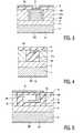
- Figure 1 shows a top plan view (with metallisation removed) while Figures 2 , 3, 4 and 5 show cross-sectional views taken along lines V-V, VI-VI, VII-VII, VIII-VIII respectively.
- the metallisation is omitted in Figure 1 to show the underlying structure.
- the semiconductor device 1 shown in Figures 1 to 5 comprises a field effect device FD.
- the semiconductor device comprises a semiconductor body 10 which, in this example, comprises a silicon substrate 2 relatively highly doped with p conductivity type impurities and a silicon epitaxial layer 3 relatively lowly doped with p- conductivity type impurities, typically boron.
- the dopant concentration of the epitaxial layer 3 may be in the range 1 x 10 16 to 2 x 10 17 cm -3 and the layer may have a thickness in the range 10 to 100 micrometres.
- the semiconductor body 10 has n conductivity type source and drain regions 4 and 5 separated by a p conductivity type body region 6 and both meeting a surface 3a of the semiconductor body.
- the source and drain regions 4 and 5 will have dopant concentrations in the range of from 1 x 10 19 cm -3 to 1 x 10 21 cm -3 and a depth of, for example, 2 to 4 micrometres.
- the body region 6 will have a dopant concentration of from 1 x 10 16 to 2 x 10 17 cm -3 and a depth of the same order as but greater than that of the source region 4.
- the field effect device FD has a gate structure 70 provided within a trench 80 for controlling a conduction channel in a conduction channel accommodation portion 60 of the body region 6.
- the body region 6 is separated from the drain region 5 by a drain drift region 50 which is relatively lowly doped with n conductivity type impurities.
- the field effect device has a central drain region 5 spaced apart by body regions from source regions 4 provided on either side of the drain region 5.
- a plurality of gate structures 70 extending parallel to one another in respective trenches 80 are provided between each source region 4 and the drain region 5.
- three gate structures 70 extend between each source region 4 and the central drain region 5. It will, however, be appreciated that there may be one, two, three or many more gate structures 70 extending parallel to one another between each source region 4 and the central drain region 5.
- Each gate structure 70 comprises an insulated gate structure having a gate conductive region 70b separated from the trench 80 by a gate dielectric layer 70a.
- Channel accommodation portions 60 of the body region 6 extend at least along side walls 80a of the trenches 8.
- each gate structure 70 is associated with a field plate 71 extending from the gate structure towards the drain region 5 over the drain drift region 50.
- Each field plate 71 is formed by an extension of the gate conductive region 70b extending over a relatively thick dielectric layer 71a through the relatively lowly doped drain drift region 50. This is achieved by forming each trench 80 so that it extends through the drain drift region 50 as well as through the body portion 6 and by controlling the thickness of the dielectric layer so that a relatively thin gate dielectric layer 70a is formed on the portion of the side walls 80a of the trench 80 adjoining a conduction channel accommodation portion 60 of the body region 6 and a relatively thick dielectric layer 71a is formed on the portions of the side walls 80a of the trench 8 extending through the drain drift region 50.
- the thickness of the dielectric on the bottom wall 80b of a trench in the drain drift region 50 may be increased in a manner similar to the thickness of the dielectric on the side walls 80a of the trench.
- the dopant concentration in the area 50a of the drain drift region beneath the trench will be equal to or lower than in the main part of the drain drift region between the insulated gate structures.
- the thickness of the dielectric layer on the bottom wall 80b of the trenches may be the same as the thickness of the gate dielectric layer 70a.
- source, drain and gate electrodes S, D and G are formed on the surface 3a in respective windows in a dielectric layer 9 so that each electrode substantially covers and makes ohmic contact with the exposed portion of the corresponding source drain or gate conductive region 4, 5 or 70b.
- the metallisation forming the gate electrode G extends over the dielectric layer 9 so that the three gate structures on one side of the drain region 5 are connected in series and the three gate structures on the other side of the drain region 5 in Figure 1 are connected in series.
- the field effect device FD is provided with edge termination which, in this example, consists of a further field plate 90 deposited onto a thick dielectric layer 91.
- the further field plate 90 is covered by a passivating layer 92 made of, for example, an insulating material such as silicon dioxide or of polycrystalline silicon.
- the further gate field plate 90 is ohmically coupled via a window in the overlying dielectric layer 9 to the gate electrode G.
- the drain drift region 50 may have a dopant concentration of 1 x 10 19 to 1 x 10 21 cm -3 and a thickness of 2 to 100 micrometres.
- the trenches 80 may have a depth of from approximately 2 micrometres to approximately 100 micrometres, dependent on the thickness of the layer in which the trenches are formed.
- the device shown in Figures 1 to 5 may be manufactured by introduction of dopants using an appropriate mask and anisotropic etching of the trenches for the gate structures or by the use of selective epitaxial deposition into a trench formed in the epitaxial layer 3 and then, if necessary, subsequent anisotropic etching of the trenches for the gate structures.
- the different thicknesses of dielectric layers in the trenches may be formed by, for example, growing a thermal oxide to the thickness required for the dielectric layers 71a, then masking the areas where dielectric of that thickness is required and anisotropically etching the exposed areas of the dielectric layer to etch the dielectric away and then growing or depositing gate oxide to the thickness required for the gate dielectric layer 70a.
- Doped polycrystalline silicon is then be deposited to form the gate conductive regions 70b and field plates 71, the dielectric layer 9 is then deposited and patterned followed by deposition and patterning of the metallisation to form the source, gate and drain electrodes S, G and D.
- a back gate electrode BG may be provided on the surface 2a of the substrate 2.
- the field effect device is provided on a silicon substrate. This need, however, not necessarily be the case and, for example, the field effect device may be provided on an insulating layer to provide a silicon on insulator type device.
- the field effect device has a stripe-like geometry with the source and drain regions being elongate and rectangular when viewed in plan and the gate structures also being elongate and rectangular when viewed in plan.
- the device shown in Figure 1 may be modified by omitting either the left hand or right hand half of the device so that only a single source and a single drain region are provided. Furthermore, the structure shown in Figure 1 may represent a unit cell that is repeated one or more times on the same semiconductor body.
- Geometries other than elongate and rectangular when viewed in plan may be adopted.
- Figure 6 shows a plan view, similar to Figure 1 (that is with top metallisation omitted), of a second embodiment of a device 1' in accordance with the present invention.
- the device 1' shown in Figure 6 differs from the device shown in plan view in Figure 1 in that a circular or elliptical geometry is adopted rather than the rectangular geometry shown in Figure 1 .
- a central circular or elliptical source region 4' is surrounded by an annular body region 6' which is itself surrounded by an annular drain drift region 50' itself surrounded by an annular drain region 5'.
- Gate structures 70' radiate outwardly from the source region 4' towards the drain region 5' so as to be equi-angularly spaced around the periphery of the source region 4'.
- Each of the insulated gate structures 70' has the same general configuration as the insulated gate structures 70 described above, that is each insulated gate structure 70' is provided in a trench 80' in which the thickness of the dielectric layer is controlled so as to provide a relatively thin gate dielectric layer 70'a on the portion of side walls of the trench 80'a adjoining a conduction channel accommodation portion 50' of the body region and a relatively thick dielectric layer 71'a on portions of the side walls 80'a of the trench 8' extending through the drain drift region 50', so that an extension of the gate conductive region 70'b provides a field plate 71'.
- the radial arrangement of the insulated gate structures 70' means that the width W of the drift region 50' between neighbouring field plates 71' increases in a radial direction towards the drain region 5'.
- a reverse blocking mode that is when voltages are applied to the source and drain electrodes but a voltage of zero volts (OV) is applied to the gate electrode to render the device conducting
- the extent of the spread of the depletion region within the drain drift region will be controlled by the dopant concentration within the drain drift region and the angle ⁇ subtended between adjacent trenches 80'.
- Figure 6 shows a line A which follows the shape of the pn junction between the source and body regions.
- the line A is a circular arc.
- a dotted line B forming a radius of a circular arc A bisects the angle ⁇ and cuts a unit cell along an axis of symmetry.
- the integral dopant concentration along the line A increases in a direction away from the centre of the device, that is towards the drain region 5', so that, when the device is in a reverse blocking mode, the amount by which the depletion region extends through the drain drift region in a direction away from the source region 4' is controlled not only by the dopant concentration within the drain drift region but also by the angle ⁇ .
- the area of drift region that has to be depleted increases with distance from the centre of the device so effectively providing a three dimensional doping gradient increasing in the direction towards the drain region.
- the angle ⁇ will be made smaller while if a device having a relatively low breakdown voltage is required, then the angle ⁇ will be increased and the radial extent of the drain drift region made smaller.
- the number of unit cells (that is the number of insulated gate structures) will depend upon the required device conductance characteristics and required reverse breakdown voltage as discussed above.
- Figure 7 shows a plan view similar to Figure 6 of a third embodiment of a device 1" in accordance with the present invention.
- the device shown in Figure 7 differs from that shown in Figure 6 in that the trenches 80" are trapezoidal rather than rectangular, that is the width (that is the dimension perpendicular to a direction radiating outwardly from the source region 4') of the trenches 8" increases in a direction towards the drain region 5'.
- the width of the gate conductive region 70"b also increases towards the drain region 5'.
- the relatively thick oxide or dielectric layer 71 "a is defined so that the field plate 71" is rectangular, that is the thickness of the relatively thick dielectric layer 71 "a, at least on the side walls 80"a of the trenches 80", increases towards the drain region 5' so that the influence of the field plate decreases towards the drain region 5'.
- Figure 8 shows a plan view similar to Figures 6 and 7 of a further embodiment of a device 1a in accordance with the invention.
- this device 1a consists of four unit cells defined by four insulated gate structures 700.
- the trenches 8" in which the insulated gate structures are formed are trapezoidal increasing in width towards the drain region 5'.
- the field plate dielectric layer 71"b is of uniform thickness so that the field plate 710 also has a width which increases towards the drain region 5'.
- Figure 9 shows a cross-sectional view taken along line X-X of Figure 8 through an insulated gate structure 700.
- this cross-sectional view differs from that shown in Figure 2 in that the thickness of the dielectric layer beneath the field plate 710 is the same as the thickness of the dielectric layer beneath the conductive gate region 71"b.
- the dopant concentration within the drift portion 50'a of the drain drift region beneath the field plate 710 is equal to or lower than the dopant concentration within the active area of the drain drift region.
- the structure shown in Figure 9 could be modified so as to provide a thicker dielectric layer beneath the field plate as in the example shown in Figure 2 .
- the insulated gate structures shown in Figures 6 and 7 will have a similar cross-section to that shown in Figure 9 .
- Figure 10 shows a top plan view similar to Figures 6 to 8 of another embodiment of a device 1b in accordance with the invention.
- the device 1b has a square geometry with a central source region 400 surrounded by a body region 600 having a generally rectangular (or diamond shape) outer perimeter itself surrounded by a drain drift region 501 again having a generally rectangular or diamond-shaped outer periphery.
- the drain drift region 501 is itself surrounded by a drain region 500 having a, in this example, circular outer periphery.
- the insulated gate structures 700 have, in this example, the same structure as shown in Figure 8 . It will, however, be appreciated that the insulated gate configuration shown in Figure 6 or 7 could also be adopted with this generally square geometry.
- any geometry which is configured such that the separation of the insulated gate structures and thus the width of the drain drift region increases in a direction from the source region to the drain region will provide the advantages discussed above with reference to Figure 6 with the angular separation ⁇ of the insulated gate structures and the drain drift region dopant concentration controlling the spread of the depletion region within the drain drift region and thus the reverse breakdown characteristics of the device.
- the device geometry shown in Figure 1 may also be modified so that the trenches are trapezoidal decreasing in width towards the drain region 5 so as to provide a drain drift region 50 whose width, and therefore effective dopant concentrations, increases towards the drain region 5.
- the conduction channel accommodation portions 60 are provided along side walls of the trenches.
- the conduction channel accommodation portions may also be provided beneath the bottom of the trenches.
- Each insulated gate structure of course extends slightly into the source region so that the conduction channel accommodation portions 60 can provide a conductive path for majority charge carriers between the source and drain drift regions. As shown, the trenches meet and slightly extend into the drain region so that the field plates extend as far as the drain region.
- edge termination described above may be omitted.
- the field effect transistor described above is a normally off or enhancement mode device.
- the present invention may be applied to normally on or depletion mode devices, in which case at least the part of the body region defining the channel accommodation portion will be of the same conductivity type as the source and drain regions 4 and 5.
- the present invention may also be applicable to MESFETs as well as to insulated gate field effect devices.
- the field effect device may be, for example, an insulated gate bipolar transistor where the drain region is of the opposite conductivity type to the source region.
- the invention may also be applied to Schottky source devices.
- the gate structure extends from one end of the trench to the other. This need not be the case.
- Figure 1 illustrates a uniform thickness for the gate dielectric layer 7a where it extends from the channel area to the source region 4.
- a greater thickness for the gate dielectric layer 7a (and/or even a different dielectric material) may be used where the gate structure 7a and 7b is bounded by the source region 4.
- the gate trench 80 extends into the drain region 5
- a greater dielectric thickness and/or even a different dielectric material may be used.
- the gate conductive region 7b substantially fills the trench providing the advantage of providing a planar surface.
- the conductive gate region need not substantially fill the trench but could be a relatively thin layer following the trench contour as described in US-A-4,835,584 .
Landscapes
- Insulated Gate Type Field-Effect Transistor (AREA)
- Electrodes Of Semiconductors (AREA)
- Die Bonding (AREA)
- Bipolar Transistors (AREA)
- Noodles (AREA)
- Thin Film Transistor (AREA)
Claims (13)
- Halbleiterbauelement aufweisend einen Halbleiterkörper und aufweisend ein Feldeffektelement
wobei der Halbleiterkörper Source- und Draingebiete (4, 5; 4', 5') aufweist,
wobei die Source- und Draingebiete beide an die gleiche Oberfläche (3a) des Halbleiterköpers reichen und
von einem Körpergebiet (6; 6') und einem Driftgebiet (50; 50') getrennt werden,
wobei das Feldeffektelement eine isolierte Gatestruktur (70; 70'; 700) aufweist, um einen Leitungskanal für Hauptladungsträger zwischen Source- und Draingebieten zu steuern, wobei die isolierte Gatestruktur mit einem sich im Halbleiterkörper erstreckenden Graben (80; 80', 80") versehen ist und ein von dem Graben durch eine Dielektrizitätsschicht getrenntes Gateleitungsgebiet (70b; 70'b; 70"b) hat, so dass ein Leitungskanalaufnahmeteil (60; 60') des Körpergebietes sich wenigstens entlang von Seitenwänden (80a; 80'a; 80"a) des Grabens und zwischen den Source- (4; 4') und Draindriftgebieten (50; 50') erstreckt,
dadurch gekennzeichnet, dass
der Graben sich von dem Sourcegebiet durch das Körpergebiet und das Draindriftgebiet (50; 50') hindurch zu dem Draingebiet erstreckt; und
die Dielektrizitätsschicht wenigstens an jenen Seitenwänden (80a; 80'a; 80"a) des Grabens, die sich von dem Sourcegebiet (4, 4') zu dem Draingebiet (5, 5') erstrecken, eine größere Dicke in dem sich in die Draindriftregion (50; 50') erstreckenden Teil als in dem verbleibenden Teil des Grabens hat, so dass eine sich in dem Graben durch das Draindriftgebiet hindurch in Richtung des Draingebiets (5; 5') erstreckende Verlängerung (71; 71'; 71"; 710) des Gateleitungsgebietes eine Feldplatte bildet. - Halbleiterbauelement nach Anspruch 1
aufweisend einer Vielzahl von isolierten Gatestrukturen (70; 70'; 700),
wobei jede mit einem jeweiligen Graben (80; 80'; 80") versehen ist und
wobei jede ein von dem Graben durch eine Dielektrizitätsschicht (70a; 70'a) getrenntes Gateleitungsgebiet (70b; 70'b; 70"b) hat, so dass ein Leitungskanalaufnahmeteil (60; 60') des Körpergebiets (6; 6') sich wenigstens entlang von Seitenwänden (80a; 80'a; 80"a) jedes Grabens erstreckt;
wobei jeder Graben sich von dem Sourcegebiet (4, 4') durch das Körpergebiet (6; 6') und das Draindriftgebiet (50; 50') hindurch zu dem Draingebiet (5, 5') erstreckt,
wobei die Dielektrizitätsschicht in jedem Graben wenigstens an jenen Seitenwänden des Grabens, die sich von dem Sourcegebiet (4, 4') zu dem Draingebiet (5, 5') erstrecken, eine größere Dicke in dem sich in die Draindriftregion erstreckenden Teil des Grabens haben, so dass eine Verlängerung (71; 71'; 71"; 710) des Gateleitungsgebiets (70b; 70'b; 70"b) eine sich in dem Draindriftgebiet (5; 5') in Richtung des Draingebiets (5; 5') erstreckende Feldplatte bildet. - Halbleiterbauelement nach Anspruch 2,
wobei sich die isolierten Gatestrukturen parallel zueinander und in einer Richtung senkrecht zur Hauptladungsträgerbewegungsrichtung durch die Leitungskanalaufnahmeteile (60) hindurch angeordnet sind. - Halbleiterbauelement nach Anspruch 2,
wobei das Sourcegebiet (4') von dem Körper- (6'), Draindrift- (50') und Draingebiet (5') umgeben ist
und die isolierten Gatestrukturen (70'; 700) so um den Umfang des Sourcegebietes (4') angeordnet sind, dass sie sich von dem Sourcegebiet (4') in Richtung des Draingebietes (5') erstrecken,
wodurch der Abstand zwischen zwei benachbarten isolierten Gatestrukturen (70'; 700) mit dem Abstand von dem Sourcegebiet zu dem Draingebiet zunimmt. - Halbleiterbauelement nach Anspruch 4,
wobei das Feldeffektbauelement eine zirkulare Geometrie hat und sich die isolierten Gatestrukturen (70'; 700) von dem Sourcegebiet (4') radial nach außen in Richtung des Draingebietes (5') erstrecken. - Halbleiterbauelement nach einem der voranstehenden Ansprüche,
wobei der oder jeder Graben (80; 80'; 80") ein rechteckiger Graben ist. - Halbleiterbauelement nach einem der Ansprüche 1 bis 5,
wobei der oder jeder Graben (80', 80") eine Breite hat, welche sich in einer Richtung von dem Sourcegebiet (4') zu dem Draingebiet (5') vergrößert. - Halbleiterbauelement nach Anspruch 7,
wobei die Dicke der Dielektrizitätsschicht in dem sich durch das Draindriftgebiet (50; 50') erstreckenden Teil jedes Grabens (80; 80'; 80") in Richtung des Draingebiets (5; 5') konstant ist. - Halbleiterbauelement nach Anspruch 7,
wobei die Dicke der Dielektrizitätsschicht (71"a) in dem sich in dem Draindriftgebiet (50') erstreckenden Teil jedes Grabens (80") und wenigstens an Seitenwänden (80"a) des Grabens (80") in Richtung des Draingebietes (5') zunimmt. - Halbleiterbauelement nach Anspruch 2,
wobei das Feldeffektbauelement eine rechteckige Geometrie mit länglichen Source- und Draingebieten hat (4 und 5) und
wobei die isolierten Gatestrukturen (70) senkrecht zu einer Richtung länglich sind, in welcher die Source- und Draingebiete länglich sind. - Halbleiterbauelement nach einem der Ansprüche 1 bis 9,
wobei der oder jeder Graben (80; 80'; 80") in einer Richtung entlang der Oberfläche zu dem Draingebiet (5; 5') hin länglich ist. - Halbleiterbauelement nach einem der voranstehenden Ansprüche,
wobei der oder jeder Graben (80; 80'; 80") erste und zweiten Enden hat und
wobei das erste Ende wenigstens teilweise von dem Sourcegebiet (4; 4') umgeben ist. - Halbleiterbauelement nach einem der Ansprüche 1 bis 11,
wobei der oder jeder Graben (80; 80'; 80") länglich ist und ein erstes und ein zweite Ende hat, wobei das erste Ende wenigstens teilweise von dem Sourcegebiet (4; 4') umgeben ist, und wobei das zweite Ende an das Draingebiet (5; 5') reicht.
Applications Claiming Priority (3)
| Application Number | Priority Date | Filing Date | Title |
|---|---|---|---|
| GB0012138 | 2000-05-20 | ||
| GBGB0012138.4A GB0012138D0 (en) | 2000-05-20 | 2000-05-20 | A semiconductor device |
| PCT/EP2001/004932 WO2001091190A1 (en) | 2000-05-20 | 2001-05-01 | A semiconductor device |
Publications (2)
| Publication Number | Publication Date |
|---|---|
| EP1290735A1 EP1290735A1 (de) | 2003-03-12 |
| EP1290735B1 true EP1290735B1 (de) | 2011-11-16 |
Family
ID=9891934
Family Applications (1)
| Application Number | Title | Priority Date | Filing Date |
|---|---|---|---|
| EP01938146A Expired - Lifetime EP1290735B1 (de) | 2000-05-20 | 2001-05-01 | Halbleiterbauelement |
Country Status (6)
| Country | Link |
|---|---|
| US (1) | US6534823B2 (de) |
| EP (1) | EP1290735B1 (de) |
| JP (1) | JP2003534666A (de) |
| AT (1) | ATE534145T1 (de) |
| GB (1) | GB0012138D0 (de) |
| WO (1) | WO2001091190A1 (de) |
Cited By (1)
| Publication number | Priority date | Publication date | Assignee | Title |
|---|---|---|---|---|
| EP2203933A2 (de) * | 2007-10-19 | 2010-07-07 | Nxp B.V. | Hochspannungshalbleiterbauelement |
Families Citing this family (27)
| Publication number | Priority date | Publication date | Assignee | Title |
|---|---|---|---|---|
| US6555873B2 (en) * | 2001-09-07 | 2003-04-29 | Power Integrations, Inc. | High-voltage lateral transistor with a multi-layered extended drain structure |
| DE10262418B3 (de) * | 2002-02-21 | 2015-10-08 | Infineon Technologies Ag | MOS-Transistoreinrichtung |
| DE10324754B4 (de) | 2003-05-30 | 2018-11-08 | Infineon Technologies Ag | Halbleiterbauelement |
| GB0314392D0 (en) * | 2003-06-20 | 2003-07-23 | Koninkl Philips Electronics Nv | Trench mos structure |
| EP1706899A4 (de) * | 2003-12-19 | 2008-11-26 | Third Dimension 3D Sc Inc | Planarisierungsverfahren zur herstellung eines superjunction-bauelements |
| DE102004064308B3 (de) | 2004-08-25 | 2018-10-31 | Infineon Technologies Austria Ag | Laterale Halbleiterdiode mit einer Feldelektrode und einer Eckstruktur |
| DE102004041198B4 (de) * | 2004-08-25 | 2016-06-09 | Infineon Technologies Austria Ag | Laterales Halbleiterbauelement mit einer Feldelektrode und einer Entladestruktur |
| DE102004047772B4 (de) * | 2004-09-30 | 2018-12-13 | Infineon Technologies Ag | Lateraler Halbleitertransistor |
| US7473966B1 (en) * | 2004-11-09 | 2009-01-06 | Blanchard Richard A | Oxide-bypassed lateral high voltage structures and methods |
| US7560359B2 (en) * | 2004-11-26 | 2009-07-14 | Samsung Electronics Co., Ltd. | Methods of forming asymmetric recesses and gate structures that fill such recesses and related methods of forming semiconductor devices that include such recesses and gate structures |
| US8183113B2 (en) * | 2005-08-24 | 2012-05-22 | Samsung Electronics Co., Ltd. | Methods of forming recessed gate structures including blocking members, and methods of forming semiconductor devices having the recessed gate structures |
| US7804150B2 (en) * | 2006-06-29 | 2010-09-28 | Fairchild Semiconductor Corporation | Lateral trench gate FET with direct source-drain current path |
| JP5280056B2 (ja) * | 2008-01-10 | 2013-09-04 | シャープ株式会社 | Mos電界効果トランジスタ |
| US8004051B2 (en) * | 2009-02-06 | 2011-08-23 | Texas Instruments Incorporated | Lateral trench MOSFET having a field plate |
| JP5656608B2 (ja) * | 2010-12-17 | 2015-01-21 | 三菱電機株式会社 | 半導体装置 |
| JP6084357B2 (ja) * | 2011-11-02 | 2017-02-22 | ルネサスエレクトロニクス株式会社 | 半導体装置 |
| US9799762B2 (en) | 2012-12-03 | 2017-10-24 | Infineon Technologies Ag | Semiconductor device and method of manufacturing a semiconductor device |
| CN105556647B (zh) | 2013-07-19 | 2017-06-13 | 日产自动车株式会社 | 半导体装置及其制造方法 |
| US9287404B2 (en) | 2013-10-02 | 2016-03-15 | Infineon Technologies Austria Ag | Semiconductor device and method of manufacturing a semiconductor device with lateral FET cells and field plates |
| US9306058B2 (en) * | 2013-10-02 | 2016-04-05 | Infineon Technologies Ag | Integrated circuit and method of manufacturing an integrated circuit |
| US9401399B2 (en) | 2013-10-15 | 2016-07-26 | Infineon Technologies Ag | Semiconductor device |
| US9496339B2 (en) * | 2014-06-02 | 2016-11-15 | Infineon Technologies Austria Ag | Semiconductor device comprising trench structures |
| DE102015105632B4 (de) * | 2015-04-14 | 2016-09-01 | Infineon Technologies Ag | Halbleitervorrichtung mit einem transistor |
| DE102016113393B4 (de) | 2016-07-20 | 2024-11-21 | Infineon Technologies Ag | Halbleitervorrichtung, die ein transistor-array und ein abschlussgebiet enthält, halbleitervorrichtung mit einem leistungstransistor in einem halbleitersubstrat und verfahren zum herstellen solch einer halbleitervorrichtung |
| TWI777225B (zh) * | 2019-08-29 | 2022-09-11 | 台灣積體電路製造股份有限公司 | 積體晶片及其形成方法 |
| CN111244160B (zh) * | 2020-01-17 | 2022-11-01 | 中国科学院微电子研究所 | 一种具有环形沟道区的mos器件及其制备方法 |
| CN117276329A (zh) * | 2023-11-20 | 2023-12-22 | 深圳天狼芯半导体有限公司 | 一种具有沟槽栅的ldmos及制备方法 |
Citations (1)
| Publication number | Priority date | Publication date | Assignee | Title |
|---|---|---|---|---|
| US5229633A (en) * | 1987-06-08 | 1993-07-20 | U.S. Philips Corporation | High voltage lateral enhancement IGFET |
Family Cites Families (9)
| Publication number | Priority date | Publication date | Assignee | Title |
|---|---|---|---|---|
| US4243997A (en) * | 1976-03-25 | 1981-01-06 | Tokyo Shibaura Electric Co., Ltd. | Semiconductor device |
| JPS61226966A (ja) * | 1985-03-30 | 1986-10-08 | Toshiba Corp | 半導体装置 |
| US4835584A (en) | 1986-11-27 | 1989-05-30 | American Telephone And Telegraph Company, At&T Bell Laboratories | Trench transistor |
| US5040034A (en) * | 1989-01-18 | 1991-08-13 | Nissan Motor Co., Ltd. | Semiconductor device |
| US5640034A (en) | 1992-05-18 | 1997-06-17 | Texas Instruments Incorporated | Top-drain trench based resurf DMOS transistor structure |
| US5434435A (en) * | 1994-05-04 | 1995-07-18 | North Carolina State University | Trench gate lateral MOSFET |
| WO1999043029A1 (de) * | 1998-02-20 | 1999-08-26 | Infineon Technologies Ag | Graben-gate-mos-transistor, dessen verwendung in einer eeprom-anordnung und verfahren zu dessen herstellung |
| JP3641547B2 (ja) * | 1998-03-25 | 2005-04-20 | 株式会社豊田中央研究所 | 横型mos素子を含む半導体装置 |
| GB9906247D0 (en) * | 1999-03-18 | 1999-05-12 | Koninkl Philips Electronics Nv | An electronic device comprising a trench gate field effect device |
-
2000
- 2000-05-20 GB GBGB0012138.4A patent/GB0012138D0/en not_active Ceased
-
2001
- 2001-05-01 AT AT01938146T patent/ATE534145T1/de active
- 2001-05-01 EP EP01938146A patent/EP1290735B1/de not_active Expired - Lifetime
- 2001-05-01 JP JP2001587486A patent/JP2003534666A/ja not_active Withdrawn
- 2001-05-01 WO PCT/EP2001/004932 patent/WO2001091190A1/en not_active Ceased
- 2001-05-18 US US09/860,358 patent/US6534823B2/en not_active Expired - Fee Related
Patent Citations (1)
| Publication number | Priority date | Publication date | Assignee | Title |
|---|---|---|---|---|
| US5229633A (en) * | 1987-06-08 | 1993-07-20 | U.S. Philips Corporation | High voltage lateral enhancement IGFET |
Cited By (1)
| Publication number | Priority date | Publication date | Assignee | Title |
|---|---|---|---|---|
| EP2203933A2 (de) * | 2007-10-19 | 2010-07-07 | Nxp B.V. | Hochspannungshalbleiterbauelement |
Also Published As
| Publication number | Publication date |
|---|---|
| GB0012138D0 (en) | 2000-07-12 |
| US20010045599A1 (en) | 2001-11-29 |
| US6534823B2 (en) | 2003-03-18 |
| JP2003534666A (ja) | 2003-11-18 |
| WO2001091190A1 (en) | 2001-11-29 |
| ATE534145T1 (de) | 2011-12-15 |
| EP1290735A1 (de) | 2003-03-12 |
Similar Documents
| Publication | Publication Date | Title |
|---|---|---|
| US6534823B2 (en) | Semiconductor device | |
| US6600194B2 (en) | Field-effect semiconductor devices | |
| EP0763259B1 (de) | Durchgriff-feldeffekttransistor | |
| EP1145326B1 (de) | Graben-gate-feldeffekttransistoren mit einer zellenstruktur | |
| US6462377B2 (en) | Insulated gate field effect device | |
| EP0948818B1 (de) | Hochdichte-graben-dmos-transistor mit grabenbodemimplantierung | |
| EP1340263B1 (de) | Graben-gate-feldeffekttransistoren und ihre herstellung | |
| EP1208600B1 (de) | Hochspannungs-halbleiteranordnung mit einer feldplattenstruktur | |
| US7489011B2 (en) | Semiconductor device containing dielectrically isolated PN junction for enhanced breakdown characteristics | |
| EP1033759B1 (de) | MOS-Anordnung mit einer vergrabenen Gate und Verfahren zur Herstellung | |
| EP1415334B1 (de) | Herstellung von halbleiteranordnungen mit schottky sperrschichten | |
| US6835993B2 (en) | Bidirectional shallow trench superjunction device with resurf region | |
| US6787872B2 (en) | Lateral conduction superjunction semiconductor device | |
| US6400003B1 (en) | High voltage MOSFET with geometrical depletion layer enhancement | |
| JP2005501408A (ja) | トレンチショットキー整流器が組み込まれたトレンチ二重拡散金属酸化膜半導体トランジスタ | |
| WO2001059846A1 (en) | Semiconductor device with voltage divider for increased reverse blocking voltage | |
| EP1295342B1 (de) | Feldeffektbauelement |
Legal Events
| Date | Code | Title | Description |
|---|---|---|---|
| PUAI | Public reference made under article 153(3) epc to a published international application that has entered the european phase |
Free format text: ORIGINAL CODE: 0009012 |
|
| 17P | Request for examination filed |
Effective date: 20021220 |
|
| AK | Designated contracting states |
Kind code of ref document: A1 Designated state(s): AT BE CH CY DE DK ES FI FR GB GR IE IT LI LU MC NL PT SE TR |
|
| RAP1 | Party data changed (applicant data changed or rights of an application transferred) |
Owner name: NXP B.V. |
|
| 17Q | First examination report despatched |
Effective date: 20081015 |
|
| RTI1 | Title (correction) |
Free format text: SEMICONDUCTOR DEVICE |
|
| GRAP | Despatch of communication of intention to grant a patent |
Free format text: ORIGINAL CODE: EPIDOSNIGR1 |
|
| GRAC | Information related to communication of intention to grant a patent modified |
Free format text: ORIGINAL CODE: EPIDOSCIGR1 |
|
| GRAS | Grant fee paid |
Free format text: ORIGINAL CODE: EPIDOSNIGR3 |
|
| GRAA | (expected) grant |
Free format text: ORIGINAL CODE: 0009210 |
|
| AK | Designated contracting states |
Kind code of ref document: B1 Designated state(s): AT BE CH CY DE DK ES FI FR GB GR IE IT LI LU MC NL PT SE TR |
|
| REG | Reference to a national code |
Ref country code: GB Ref legal event code: FG4D |
|
| REG | Reference to a national code |
Ref country code: CH Ref legal event code: EP |
|
| REG | Reference to a national code |
Ref country code: IE Ref legal event code: FG4D |
|
| REG | Reference to a national code |
Ref country code: DE Ref legal event code: R096 Ref document number: 60145674 Country of ref document: DE Effective date: 20120126 |
|
| REG | Reference to a national code |
Ref country code: NL Ref legal event code: VDEP Effective date: 20111116 |
|
| PG25 | Lapsed in a contracting state [announced via postgrant information from national office to epo] |
Ref country code: SE Free format text: LAPSE BECAUSE OF FAILURE TO SUBMIT A TRANSLATION OF THE DESCRIPTION OR TO PAY THE FEE WITHIN THE PRESCRIBED TIME-LIMIT Effective date: 20111116 Ref country code: BE Free format text: LAPSE BECAUSE OF FAILURE TO SUBMIT A TRANSLATION OF THE DESCRIPTION OR TO PAY THE FEE WITHIN THE PRESCRIBED TIME-LIMIT Effective date: 20111116 Ref country code: NL Free format text: LAPSE BECAUSE OF FAILURE TO SUBMIT A TRANSLATION OF THE DESCRIPTION OR TO PAY THE FEE WITHIN THE PRESCRIBED TIME-LIMIT Effective date: 20111116 Ref country code: GR Free format text: LAPSE BECAUSE OF FAILURE TO SUBMIT A TRANSLATION OF THE DESCRIPTION OR TO PAY THE FEE WITHIN THE PRESCRIBED TIME-LIMIT Effective date: 20120217 Ref country code: PT Free format text: LAPSE BECAUSE OF FAILURE TO SUBMIT A TRANSLATION OF THE DESCRIPTION OR TO PAY THE FEE WITHIN THE PRESCRIBED TIME-LIMIT Effective date: 20120316 |
|
| PG25 | Lapsed in a contracting state [announced via postgrant information from national office to epo] |
Ref country code: CY Free format text: LAPSE BECAUSE OF FAILURE TO SUBMIT A TRANSLATION OF THE DESCRIPTION OR TO PAY THE FEE WITHIN THE PRESCRIBED TIME-LIMIT Effective date: 20111116 |
|
| PG25 | Lapsed in a contracting state [announced via postgrant information from national office to epo] |
Ref country code: DK Free format text: LAPSE BECAUSE OF FAILURE TO SUBMIT A TRANSLATION OF THE DESCRIPTION OR TO PAY THE FEE WITHIN THE PRESCRIBED TIME-LIMIT Effective date: 20111116 |
|
| PGFP | Annual fee paid to national office [announced via postgrant information from national office to epo] |
Ref country code: DE Payment date: 20120531 Year of fee payment: 12 |
|
| PG25 | Lapsed in a contracting state [announced via postgrant information from national office to epo] |
Ref country code: IT Free format text: LAPSE BECAUSE OF FAILURE TO SUBMIT A TRANSLATION OF THE DESCRIPTION OR TO PAY THE FEE WITHIN THE PRESCRIBED TIME-LIMIT Effective date: 20111116 |
|
| REG | Reference to a national code |
Ref country code: AT Ref legal event code: MK05 Ref document number: 534145 Country of ref document: AT Kind code of ref document: T Effective date: 20111116 |
|
| PLBE | No opposition filed within time limit |
Free format text: ORIGINAL CODE: 0009261 |
|
| STAA | Information on the status of an ep patent application or granted ep patent |
Free format text: STATUS: NO OPPOSITION FILED WITHIN TIME LIMIT |
|
| 26N | No opposition filed |
Effective date: 20120817 |
|
| REG | Reference to a national code |
Ref country code: DE Ref legal event code: R097 Ref document number: 60145674 Country of ref document: DE Effective date: 20120817 |
|
| PG25 | Lapsed in a contracting state [announced via postgrant information from national office to epo] |
Ref country code: MC Free format text: LAPSE BECAUSE OF NON-PAYMENT OF DUE FEES Effective date: 20120531 |
|
| REG | Reference to a national code |
Ref country code: CH Ref legal event code: PL |
|
| PG25 | Lapsed in a contracting state [announced via postgrant information from national office to epo] |
Ref country code: AT Free format text: LAPSE BECAUSE OF FAILURE TO SUBMIT A TRANSLATION OF THE DESCRIPTION OR TO PAY THE FEE WITHIN THE PRESCRIBED TIME-LIMIT Effective date: 20111116 Ref country code: LI Free format text: LAPSE BECAUSE OF NON-PAYMENT OF DUE FEES Effective date: 20120531 Ref country code: CH Free format text: LAPSE BECAUSE OF NON-PAYMENT OF DUE FEES Effective date: 20120531 |
|
| REG | Reference to a national code |
Ref country code: IE Ref legal event code: MM4A |
|
| PG25 | Lapsed in a contracting state [announced via postgrant information from national office to epo] |
Ref country code: ES Free format text: LAPSE BECAUSE OF FAILURE TO SUBMIT A TRANSLATION OF THE DESCRIPTION OR TO PAY THE FEE WITHIN THE PRESCRIBED TIME-LIMIT Effective date: 20120227 Ref country code: IE Free format text: LAPSE BECAUSE OF NON-PAYMENT OF DUE FEES Effective date: 20120501 |
|
| PG25 | Lapsed in a contracting state [announced via postgrant information from national office to epo] |
Ref country code: FI Free format text: LAPSE BECAUSE OF FAILURE TO SUBMIT A TRANSLATION OF THE DESCRIPTION OR TO PAY THE FEE WITHIN THE PRESCRIBED TIME-LIMIT Effective date: 20111116 |
|
| PG25 | Lapsed in a contracting state [announced via postgrant information from national office to epo] |
Ref country code: DE Free format text: LAPSE BECAUSE OF NON-PAYMENT OF DUE FEES Effective date: 20131203 |
|
| REG | Reference to a national code |
Ref country code: DE Ref legal event code: R119 Ref document number: 60145674 Country of ref document: DE Effective date: 20131203 |
|
| PG25 | Lapsed in a contracting state [announced via postgrant information from national office to epo] |
Ref country code: TR Free format text: LAPSE BECAUSE OF FAILURE TO SUBMIT A TRANSLATION OF THE DESCRIPTION OR TO PAY THE FEE WITHIN THE PRESCRIBED TIME-LIMIT Effective date: 20111116 |
|
| PG25 | Lapsed in a contracting state [announced via postgrant information from national office to epo] |
Ref country code: LU Free format text: LAPSE BECAUSE OF NON-PAYMENT OF DUE FEES Effective date: 20120501 |
|
| PGFP | Annual fee paid to national office [announced via postgrant information from national office to epo] |
Ref country code: GB Payment date: 20140425 Year of fee payment: 14 |
|
| PGFP | Annual fee paid to national office [announced via postgrant information from national office to epo] |
Ref country code: FR Payment date: 20140424 Year of fee payment: 14 |
|
| GBPC | Gb: european patent ceased through non-payment of renewal fee |
Effective date: 20150501 |
|
| REG | Reference to a national code |
Ref country code: FR Ref legal event code: ST Effective date: 20160129 |
|
| PG25 | Lapsed in a contracting state [announced via postgrant information from national office to epo] |
Ref country code: GB Free format text: LAPSE BECAUSE OF NON-PAYMENT OF DUE FEES Effective date: 20150501 |
|
| PG25 | Lapsed in a contracting state [announced via postgrant information from national office to epo] |
Ref country code: FR Free format text: LAPSE BECAUSE OF NON-PAYMENT OF DUE FEES Effective date: 20150601 |