EP1289281A1 - Image pickup device, and image pickup device assembling method - Google Patents
Image pickup device, and image pickup device assembling method Download PDFInfo
- Publication number
- EP1289281A1 EP1289281A1 EP01906306A EP01906306A EP1289281A1 EP 1289281 A1 EP1289281 A1 EP 1289281A1 EP 01906306 A EP01906306 A EP 01906306A EP 01906306 A EP01906306 A EP 01906306A EP 1289281 A1 EP1289281 A1 EP 1289281A1
- Authority
- EP
- European Patent Office
- Prior art keywords
- circuit board
- barrel
- leg
- imaging apparatus
- joining
- Prior art date
- Legal status (The legal status is an assumption and is not a legal conclusion. Google has not performed a legal analysis and makes no representation as to the accuracy of the status listed.)
- Withdrawn
Links
Images



Classifications
-
- H—ELECTRICITY
- H04—ELECTRIC COMMUNICATION TECHNIQUE
- H04N—PICTORIAL COMMUNICATION, e.g. TELEVISION
- H04N23/00—Cameras or camera modules comprising electronic image sensors; Control thereof
- H04N23/50—Constructional details
- H04N23/55—Optical parts specially adapted for electronic image sensors; Mounting thereof
-
- H—ELECTRICITY
- H04—ELECTRIC COMMUNICATION TECHNIQUE
- H04N—PICTORIAL COMMUNICATION, e.g. TELEVISION
- H04N23/00—Cameras or camera modules comprising electronic image sensors; Control thereof
- H04N23/50—Constructional details
- H04N23/54—Mounting of pick-up tubes, electronic image sensors, deviation or focusing coils
-
- H—ELECTRICITY
- H10—SEMICONDUCTOR DEVICES; ELECTRIC SOLID-STATE DEVICES NOT OTHERWISE PROVIDED FOR
- H10F—INORGANIC SEMICONDUCTOR DEVICES SENSITIVE TO INFRARED RADIATION, LIGHT, ELECTROMAGNETIC RADIATION OF SHORTER WAVELENGTH OR CORPUSCULAR RADIATION
- H10F39/00—Integrated devices, or assemblies of multiple devices, comprising at least one element covered by group H10F30/00, e.g. radiation detectors comprising photodiode arrays
- H10F39/011—Manufacture or treatment of image sensors covered by group H10F39/12
- H10F39/024—Manufacture or treatment of image sensors covered by group H10F39/12 of coatings or optical elements
-
- H—ELECTRICITY
- H10—SEMICONDUCTOR DEVICES; ELECTRIC SOLID-STATE DEVICES NOT OTHERWISE PROVIDED FOR
- H10F—INORGANIC SEMICONDUCTOR DEVICES SENSITIVE TO INFRARED RADIATION, LIGHT, ELECTROMAGNETIC RADIATION OF SHORTER WAVELENGTH OR CORPUSCULAR RADIATION
- H10F39/00—Integrated devices, or assemblies of multiple devices, comprising at least one element covered by group H10F30/00, e.g. radiation detectors comprising photodiode arrays
- H10F39/80—Constructional details of image sensors
- H10F39/804—Containers or encapsulations
-
- H—ELECTRICITY
- H10—SEMICONDUCTOR DEVICES; ELECTRIC SOLID-STATE DEVICES NOT OTHERWISE PROVIDED FOR
- H10F—INORGANIC SEMICONDUCTOR DEVICES SENSITIVE TO INFRARED RADIATION, LIGHT, ELECTROMAGNETIC RADIATION OF SHORTER WAVELENGTH OR CORPUSCULAR RADIATION
- H10F39/00—Integrated devices, or assemblies of multiple devices, comprising at least one element covered by group H10F30/00, e.g. radiation detectors comprising photodiode arrays
- H10F39/80—Constructional details of image sensors
- H10F39/806—Optical elements or arrangements associated with the image sensors
-
- H—ELECTRICITY
- H10—SEMICONDUCTOR DEVICES; ELECTRIC SOLID-STATE DEVICES NOT OTHERWISE PROVIDED FOR
- H10F—INORGANIC SEMICONDUCTOR DEVICES SENSITIVE TO INFRARED RADIATION, LIGHT, ELECTROMAGNETIC RADIATION OF SHORTER WAVELENGTH OR CORPUSCULAR RADIATION
- H10F77/00—Constructional details of devices covered by this subclass
- H10F77/40—Optical elements or arrangements
- H10F77/407—Optical elements or arrangements indirectly associated with the devices
-
- H—ELECTRICITY
- H10—SEMICONDUCTOR DEVICES; ELECTRIC SOLID-STATE DEVICES NOT OTHERWISE PROVIDED FOR
- H10F—INORGANIC SEMICONDUCTOR DEVICES SENSITIVE TO INFRARED RADIATION, LIGHT, ELECTROMAGNETIC RADIATION OF SHORTER WAVELENGTH OR CORPUSCULAR RADIATION
- H10F77/00—Constructional details of devices covered by this subclass
- H10F77/50—Encapsulations or containers
Definitions
- the present invention relates to imaging apparatus such as a monitoring camera, a camera for medical use and a vehicle-mounted camera downsized using a semiconductor-imaging device.
- the imaging apparatus that uses a conventional semiconductor device has combined components such as a lens, a semiconductor-imaging device and an LSI into case or a structure respectively.
- the printed circuit board of the apparatus has a form of a plane on which components necessary for driving the semiconductor-imaging device are mounted.
- the present invention solves the above problems and provides imaging apparatus that allows further downsizing and assembling using an automatic machine and its assembling method.
- Imaging apparatus of the invention has a semiconductor imaging device on the surface and comprises a three-dimensional printed circuit board above the semiconductor imaging device. With this configuration, all the components necessary for the imaging apparatus can be integrated on a three-dimensional printed circuit board for downsizing.
- Imaging apparatus of the invention comprises a three-dimensional circuit board having a leg and a cylindrical barrel provided on the leg, a semiconductor imaging device attached on the back of the leg and a lens, supported inside the barrel, to impinge a light onto the semiconductor imaging device. With this configuration, dislocation on the optical axis between the semiconductor device and the lens is reduced.
- Imaging apparatus of the invention is characterized in that the three-dimensional circuit board includes a barrel of a bottomed cylinder shape supporting the lens, a leg connected to the barrel, inside of which is formed the wiring pattern and an opening formed at the boundary between the barrel and the leg, that the optical filter is arranged above the opening of the three-dimensional circuit board, and that the semiconductor imaging device and the on-chip components are arranged below the opening.
- the three-dimensional circuit board includes a barrel of a bottomed cylinder shape supporting the lens, a leg connected to the barrel, inside of which is formed the wiring pattern and an opening formed at the boundary between the barrel and the leg, that the optical filter is arranged above the opening of the three-dimensional circuit board, and that the semiconductor imaging device and the on-chip components are arranged below the opening.
- Imaging apparatus of the invention is characterized in that the three-dimensional circuit board comprises a recessed shoulder where a wiring pattern is formed inside of the leg and that on the recessed shoulder is arranged a printed circuit board with an LSI and on-chip components joined on one surface or both surfaces. With this configuration, it is possible to add further features to the imaging apparatus.
- Imaging apparatus of the invention is characterized in that the three-dimensional circuit board has a wiring pattern for directly providing an electric connection between the three-dimensional circuit board and another printed circuit board on the bottom of the leg.
- the three-dimensional circuit board has a wiring pattern for directly providing an electric connection between the three-dimensional circuit board and another printed circuit board on the bottom of the leg.
- Imaging apparatus of the invention is characterized in that the three-dimensional circuit board comprises a plurality of adhesive injection grooves for injecting an adhesive on the upper area of the inner circumference of the barrel.
- Imaging apparatus of the invention is characterized in that the inner circumference of the barrel of the three-dimensional circuit board is formed while tapering downward adjacent to the adhesive injection grooves. With this configuration, it is possible to uniformly permeate an adhesive onto the periphery of the lens on the inner circumference of the barrel to assure precise bonding. It is also possible to provide a structure whereby a lens is easily inserted into a three-dimensional circuit board by using an automatic machine from above or when a three-dimensional circuit board is elevated from beneath to attach the three-dimensional circuit board to the lens in fixed position.
- Imaging apparatus of the invention is characterized in that the adhesive is black.
- the adhesive is black.
- Imaging apparatus of the invention is characterized in that in the lower area of the barrel of the three-dimensional circuit board is provided an adhesive reservoir.
- Imaging apparatus of the invention is characterized in that the sections other than the effective section of the lens on the front of the lens are masked. With this configuration, it is possible to prevent an incident light from a section other than the effective section of the lens thus preventing distortion of a picture or degrading of picture quality caused by irregular reflection.
- Imaging apparatus of the invention is characterized in that the an optical filter is omitted from the foregoing configuration.
- imaging apparatus fit for a specific purpose of use, that is, imaging apparatus that is sensitive enough to detect in the nighttime the basic signal Y of a picture alone, or a sensor that can extract a video signal in the infrared region.
- a imaging apparatus assembling method of the invention is characterized in that, with respect to a three-dimensional circuit board having a barrel of a bottomed cylinder shape, a leg connected to the barrel, inside of which is formed a wiring pattern and an opening formed at the boundary between the barrel and the leg, the method comprises a step of joining a lens with the inner circumference of the barrel, a step of joining a semiconductor imaging device with the wiring pattern so as to block the opening from the back of the leg, and a step of joining on-chip components with the wiring pattern.
- a imaging apparatus assembling method of the invention is characterized in that, with respect to a three-dimensional circuit board having a barrel of a bottomed cylinder shape, a leg connected to the barrel, inside of which is formed a wiring pattern and an opening formed at the boundary between the barrel and the leg, the method comprises a step of joining a lens with the inner circumference of the barrel, a step of joining a semiconductor imaging device with the wiring pattern so as to block the opening from the back of the leg, a step of joining on-chip components with the wiring pattern, and a step of joining with the recessed shoulder a printed circuit board with an LSI and on-chip components joined in advance on one surface or both surfaces.
- a imaging apparatus assembling method of the invention is characterized in that, with respect to a three-dimensional circuit board having a barrel of a bottomed cylinder shape, a leg connected to the barrel, inside of which is formed a wiring pattern and an opening formed at the boundary between the barrel and the leg, the method comprises a step of joining an optical filter so as to block the opening from the barrel side, a step of joining a lens with the inner circumference of the barrel, a step of joining a semiconductor imaging device with the wiring pattern so as to block the opening from the back of the leg, and a step of joining on-chip components with the wiring pattern.
- a imaging apparatus assembling method of the invention is characterized in that, with respect to a three-dimensional circuit board having a barrel of a bottomed cylinder shape, a leg connected to the barrel, inside of which is formed a wiring pattern and an opening formed at the boundary between the barrel and the leg, the method comprises a step of joining an optical filter so as to block the opening from the barrel side, a step of joining a lens with the inner circumference of the barrel, a step of joining a semiconductor imaging device with the wiring pattern so as to block the opening from the back of the leg, a step of joining on-chip components with the wiring pattern, and a step of joining with the recessed shoulder a printed circuit board with an LSI and on-chip components joined in advance on one surface or both surfaces.
- a imaging apparatus assembling method of the invention is characterized in that the method comprises a step of joining an assembled three-dimensional circuit board to another printed circuit board via a wiring pattern formed on the bottom of its leg.
- the method comprises a step of joining an assembled three-dimensional circuit board to another printed circuit board via a wiring pattern formed on the bottom of its leg.
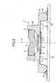
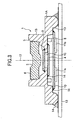
- a numeral 1 represents a three-dimensional circuit board, 1A a leg, 1B a barrel, 1C an opening, 1D a recessed shoulder, 2 a lens, 3 an optical filter, 4 a semiconductor imaging device, 5 bonding points (adhesive injection grooves), 6 a lens mask, 7 an adhesive reservoir, 8 on-chip components, 9 an adhesive, 10 a printed circuit board, 11a an LSI, 11b on-chip components, 12 a dropping pipet, 13 a printed circuit board, 14 solder, 15 a taper, 16 incident lights, 17 an optical axis, 18 a bottom of a three-dimensional circuit board, 19 a side of a three-dimensional circuit board, 22 a pattern, and 23 a video amplifier circuit.
- Fig. 1 is a perspective view showing the first embodiment of imaging apparatus according to the invention.
- Fig. 2 is a sectional view thereof.
- a three-dimensional circuit board 1 is composed of a leg 1A having rectangular frustum shape and a barrel 1B thereon having the shape of a bottomed cylinder, and an opening 1C is formed at the boundary between the leg 1A and the barrel 1B and a wiring pattern 22 is formed on the back side of the leg 1A.
- a lens 2 Onto the inner circumference of the barrel 1B of the three-dimensional circuit board 1 is fit a lens 2, about whose optical axis 17 is arranged an optical filter 3 above the opening 1C, below which are arranged a semiconductor imaging device 4 and on-chip components 8.
- a three-dimensional circuit board 1 Beneath the three-dimensional circuit board is arranged a printed circuit board 13 as a main circuit board of a portable telephone set, a PC or various sensors to which the three-dimensional circuit board 1 is attached.
- An optical filter 3 is fixed to the three-dimensional circuit board 1 from above, a lens 2 equipped with a lens mask 6 in advance on the surface is attached, then the lens 2 is fixed by injecting an adhesive from bonding points (adhesive injection grooves) 5 formed on the inner periphery of the barrel 1. An excess volume of the injected adhesive is stored in the adhesive reservoir 7 below the injection point 5.
- a semiconductor imaging device 4 an LSI or on-chip components 8 such as a resistor and a capacitor are electrically connected to a pattern 22 by way of soldering 14, a conductive adhesive, or ultrasound joint, etc. and a leg 1A is electrically connected to the pattern of a printed circuit board 13 via the pattern 22 by way of soldering, a conductive adhesive, or ultrasound joint, etc.
- Embodiment 1 of the invention it is possible to provide a compact, lightweight and rigid structure by arranging the lens 2 on the three-dimensional circuit board 1 and arranging the optical filter 3 and the semiconductor imaging device 4 on the optical axis 17 of the lens 2, and by integrally fixing the on-chip components 8 to the pattern 22 of the three-dimensional printed circuit board 1.
- This approach allows assembly by an automatic machine and is fit for mass production.
- the on-chip components 8 on the three-dimensional printed circuit board 1 to perform driving of the semiconductor imaging device 4 and de-coupling of circuits, it is possible to do without a lead wire of a length corresponding to wiring to the drive circuit for the semiconductor imaging device 4 and components mounted on the circuit board thus providing a simple structure, thereby reducing a round waveform of a clock signal flowing in the lead wire as well as reducing unwanted radiation by way of de-coupling of circuits.
- Fig. 3 is a sectional view of imaging apparatus in Embodiment 2 of the invention. For simplicity, similar members to those in Embodiment 1 are assigned the similar signs.
- a three-dimensional printed circuit board 1 is composed of a leg 1A having a rectangular frustum shape and a barrel 1B thereon having the shape of a bottomed cylinder, and an opening 1C is formed at the boundary between the leg 1A and the barrel 1B and a recessed shoulder 1D is formed inside the leg 1A.
- a wiring pattern 22 On the back-side of the leg 1A including the recessed shoulder 1D is formed a wiring pattern 22.
- a lens 2 Onto the inner circumference of the barrel 1B of the three-dimensional circuit board 1 is fit a lens 2, about whose optical axis 17 is arranged an optical filter above the opening 1C, below which are arranged a semiconductor imaging device 4 and on-chip components 8.
- a printed circuit board 10 On the recessed shoulder 1D beneath is arranged a printed circuit board 10 mounting an LSI 11a and on-chip components 11b on one surface or both surfaces, and finally a printed circuit board of a portable telephone set, etc. is arranged.
- An optical filter 3 is fixed to the three-dimensional circuit board 1 from above, a lens 2 equipped with a lens mask 6 in advance on the surface is attached, then the lens 2 is fixed by injecting an adhesive from bonding points 5 formed on the inner periphery of the barrel 1B. An excess volume of the injected adhesive is stored in the adhesive reservoir 7 below the injection point 5.
- a semiconductor imaging device 4 an LSI or on-chip components 8 such as a resistor and a capacitor are electrically connected to a pattern 22 by way of soldering 14, a conductive adhesive, or ultrasound joint, etc.
- a printed circuit board 10 is electrically connected to the pattern 22 of the recessed shoulder 1D by way of soldering 14, and finally a leg 1A is electrically connected to the pattern of a printed circuit board 13 via the pattern 22 by way of soldering, a conductive adhesive, or ultrasound joint, etc.
- Embodiment 2 of the invention it is possible to add further features to the imaging apparatus on top of the advantages of Embodiment 1 by arranging the lens 2 on the three-dimensional circuit board 1 and arranging the optical filter 3 and the semiconductor imaging device 4 on the optical axis 17 of the lens 2, and by integrally fixing the printed circuit board 10 mounting the LSI 11a and on-chip components 8 to the pattern 22 of the three-dimensional circuit board 1.
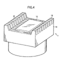
- Fig. 4 shows the bottom of the three-dimensional circuit board 1.
- the pattern 22 where the semiconductor imaging device 4 the printed circuit board 10 are electrically connected is formed by way of printing or bonding along a bottom 18 of the three-dimensional circuit board 1 and so as to reach a side 19 of the three-dimensional circuit board.
- the bottom 18 of the three-dimensional circuit board is arranged on the printed circuit board 13 for the application and electrically joined with the printed circuit board 13 by way of soldering 14, a conductive adhesive, or ultrasound joint, etc., and a video signal converted to an electric signal by the semiconductor imaging device is output to the main body of the application.
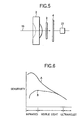
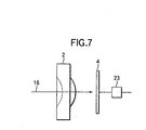
- Fig. 5 shows an optical system in the aforementioned embodiments.
- Incident lights 16 are condensed d by a lens 2, passes through an optical filter 3 that suppresses the sensitivity in the infrared spectrum, and impinges on the semiconductor imaging device 4.
- a CCD as a representative semiconductor imaging device 4 shows a flat sensitivity characteristic in the visible light region as the characteristic B obtained by passing through the optical filter 3, amplified by a video amplifier circuit 23 and corresponds to a color picture as a video signal of a flat characteristic.
- the characteristic A without the optical filter 3 shows an extremely high sensitivity in the infrared region so that the imaging apparatus can be used for imaging pictures in a dark place or as an infrared sensor by utilizing the sensitivity in the infrared region when imaging an object in a dark place.
- the imaging apparatus By removing the filter 3 for suppressing the sensitivity in the infrared region and configuring the imaging apparatus by the lens 2 and the semiconductor imaging device 4, it is possible to use the imaging apparatus as high-sensitivity imaging apparatus or an infrared sensor thus enhancing the application range of the imaging apparatus.
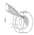
- Fig. 8 shows a method for fixing by bonding a lens 2 with a three-dimensional circuit board 1 in the embodiments.
- the structure shown comprises four bonding points (adhesive injection grooves) 5 inside the location where the lens 2 of the three-dimensional circuit board 1 is inserted thus facilitating the bonding work.
- the number of bonding points 5 is increased/decreased depending on the viscosity of the adhesive 9.
- the adhesive 9 is less viscous, the number of bonding points 5 is decreased and the adhesive 9 is injected in the form of instillation 9a, which forms adhesive spread 9b to bond the lens 2 with the three-dimensional circuit board 1.
- an appropriate volume of the adhesive 9 is injected in the form of instillation 9a from a plurality of bonding points 5.
- This structure is fit for effectively performing the instillation 9a from the dropping pipet 12 when imaging apparatus is successively produced using an automatic machine.
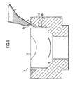
- Fig. 9 shows a structure where the inner periphery of the three-dimensional circuit board 1 is a taper 15 so that the adhesive 9 may permeate into the boundary between the lens 2 and the three-dimensional circuit board 1 when the lens 2 is bonded with the three-dimensional circuit board 1.
- the instillation 9a injected from bonding points 5 in successive production of imaging apparatus flows along the taper 15 to form the adhesive spread 9b and is applied uniformly in the peripheral of the lens 2.
- the taper 15 can be used to give a margin to the insertion of an automatic machine when the lens 2 is attached in place from above, in successive production of imaging apparatus. In other words, it is possible to insert the lens 2 from above with good margin while following the taper.
- Fig. 10 shows a structure where the adverse effects on a picture caused by irregular reflection are minimized.
- incident lights 16 are impinged and condensed by the lens 2 and focused on the semiconductor imaging device 4
- an irregularly reflected light 16a caused by dust on the surface of the lens 2 or irregularity of lights inside the lens 2 impinges on a lens side 2a and reflects thereon, which may interfere with the incident lights 16 or reach the semiconductor imaging device 4 thus causing distortion or disturbances in a picture.
- a dark (black) colored adhesive 9 is used for bonding on the outer surface of the lens 2 thus suppressing reflection of light on the lens side 2a. This allows an optical signal to suppress reflection of irregularly reflected light 16a to be output from the lens side 2a to the semiconductor imaging device 4.
- Fig. 11 shows a structure that prevents seeping of an excess volume of the adhesive 9 through the inside of the three-dimensional circuit board.
- the adhesive 9a drops inside the three-dimensional circuit board 1 thus forming seeping 9c from the lens contact surface 1a thus contaminating the inside.
- an adhesive reservoir 7 is provided in the lower area of the inner periphery of the barrel of the three-dimensional circuit board 1.
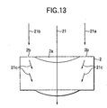
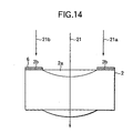
- Fig. 12 is a structure where the adverse effects on a picture caused by lights impinging on the sections other than the effective lens section are minimized.
- the lens 2 is more lightweight than a glass lens and is often manufactured by way of resin molding in order to adjust the refractive index as an aspheric lens.
- a resin-molded lens as shown in Fig. 13, when incident lights 21a, 21b impinge on a plane 2b separate from the effective lens section, the lights that impinged enter the lens due to irregular reflection on the lens surface, such as an irregularly reflected light 21c, thus interfering with the incident lights 21 or reaching the semiconductor imaging device 4, which may distort the picture or degrade the picture quality otherwise.
- the structure is equipped with a lens mask 6 by way of a black system coating or metal material onto the plane 2b, so that lights may not impinge from the plane 2b separate from the effective lens section 2a of the lens 2.
- the invention has a structure where a three-dimensional circuit board is provided having a wiring pattern for connecting a semiconductor imaging device and on-chip components, and a lens, as well as an optical filter and the semiconductor imaging device arranged on the optical axis of the lens are integrally incorporated on the three-dimensional circuit board. It is possible to provide a compact, lightweight and rigid imaging apparatus where all the components necessary for imaging apparatus are integrated on the three-dimensional circuit board, as well as implement an assembling method that allows automatic mounting of components and excellent in terms of mass production.
Landscapes
- Engineering & Computer Science (AREA)
- Multimedia (AREA)
- Signal Processing (AREA)
- Transforming Light Signals Into Electric Signals (AREA)
- Studio Devices (AREA)
- Solid State Image Pick-Up Elements (AREA)
- Lens Barrels (AREA)
Abstract
Description
Claims (16)
- Imaging apparatus comprising:a semiconductor imaging device on a surface of the imaging apparatus; anda three-dimensional circuit board above said semiconductor imaging device.
- Imaging apparatus comprising:a three-dimensional circuit board having a leg and a cylindrical barrel provided on the leg;a semiconductor imaging device attached on back of said leg; anda lens, supported inside said barrel, to impinge a light onto said semiconductor imaging device.
- Imaging apparatus according to claim 1 or 2, characterized in that said three-dimensional circuit board includes:a barrel of a bottomed cylinder shape supporting said lens;a leg connected to said barrel, inside of which is formed said wiring pattern; andan opening formed at the boundary between said barrel and the leg,
that said optical filter is arranged above said opening of said three-dimensional circuit board, and that said semiconductor imaging device and said on-chip components are arranged below said opening. - Imaging apparatus according to claim 1 or 2, characterized in that said three-dimensional circuit board comprises a recessed shoulder where a wiring pattern is formed inside said leg and that on said recessed shoulder is arranged a printed circuit board with an LSI and on-chip components joined on one surface or both surfaces.
- Imaging apparatus according to claim 3, characterized in that said three-dimensional circuit board has a wiring pattern for directly providing an electric connection between said three-dimensional circuit board and another printed circuit board on the bottom of said leg.
- Imaging apparatus according to claim 5, characterized in that said three-dimensional circuit board has a plurality of adhesive injection grooves for injecting an adhesive on the upper area of the inner circumference of said barrel.
- Imaging apparatus according to claim 6, characterized in that the inner circumference of said barrel of said three-dimensional circuit board is formed while tapering downward adjacent to said adhesive injection grooves.
- Imaging apparatus according to claim 6 or 7, characterized in that said adhesive is black.
- Imaging apparatus according to any one of the claims 6 through 8, characterized in that in the lower area of said barrel of said three-dimensional circuit board is provided an adhesive reservoir.
- Imaging apparatus according to any one of the claims 1 through 9, characterized in that the sections other than the effective section of the lens on the front of the lens are masked.
- Imaging apparatus according to any one of the claims 1 through 10, characterized in that the said optical filter is omitted.
- A imaging apparatus assembling method characterized in that, with respect to a three-dimensional circuit board having a barrel of a bottomed cylinder shape, a leg connected to said barrel inside of which is formed a wiring pattern and an opening formed at the boundary between said barrel and the leg, said method comprises a step of joining a lens with the inner circumference of said barrel, a step of joining a semiconductor imaging device with said wiring pattern so as to block said opening from the back of said leg, and a step of joining on-chip components with said wiring pattern.
- A imaging apparatus assembling method characterized in that, with respect to a three-dimensional circuit board having a barrel of a bottomed cylinder shape, a leg connected to said barrel, inside of which is formed a wiring pattern and an opening formed at the boundary between said barrel and the leg, said method comprises a step of joining a lens with the inner circumference of said barrel, a step of joining a semiconductor imaging device with said wiring pattern so as to block said opening from the back of said leg, a step of joining on-chip components with said wiring pattern, and a step of joining with said recessed shoulder a printed circuit board with an LSI and on-chip components joined in advance on one surface or both surfaces.
- A imaging apparatus assembling method characterized in that, with respect to a three-dimensional circuit board having a barrel of a bottomed cylinder shape, a leg connected to said barrel, inside of which is formed a wiring pattern and an opening formed at the boundary between said barrel and the leg, said method comprises a step of joining an optical filter so as to block said opening from said barrel side, a step of joining a lens with the inner circumference of said barrel, a step of joining a semiconductor imaging device with said wiring pattern so as to block said opening from the back of said leg, and a step of joining on-chip components with said wiring pattern.
- A imaging apparatus assembling method characterized in that, with respect to a three-dimensional circuit board having a barrel of a bottomed cylinder shape, a leg connected to said barrel, inside of which is formed a wiring pattern and an opening formed at the boundary between said barrel and the leg, said method comprises a step of joining an optical filter so as to block said opening from said barrel side, a step of joining a lens with the inner circumference of said barrel, a step of joining a semiconductor imaging device with said wiring pattern so as to block said opening from the back of said leg, a step of joining on-chip components with said wiring pattern, and a step of joining with said recessed shoulder a printed circuit board with an LSI and on-chip components joined in advance on one surface or both surfaces.
- A imaging apparatus assembling method according to any one of the claims 12 through 15 characterized in that said method comprises a step of joining an assembled three-dimensional circuit board to another printed circuit board via a wiring pattern formed on the bottom of its leg.
Applications Claiming Priority (3)
| Application Number | Priority Date | Filing Date | Title |
|---|---|---|---|
| JP2000053400A JP4004705B2 (en) | 2000-02-29 | 2000-02-29 | Imaging device and imaging device assembling method |
| JP2000053400 | 2000-02-29 | ||
| PCT/JP2001/001415 WO2001065836A1 (en) | 2000-02-29 | 2001-02-26 | Image pickup device, and image pickup device assembling method |
Publications (2)
| Publication Number | Publication Date |
|---|---|
| EP1289281A1 true EP1289281A1 (en) | 2003-03-05 |
| EP1289281A4 EP1289281A4 (en) | 2006-06-14 |
Family
ID=18574792
Family Applications (1)
| Application Number | Title | Priority Date | Filing Date |
|---|---|---|---|
| EP01906306A Withdrawn EP1289281A4 (en) | 2000-02-29 | 2001-02-26 | IMAGE TAKING DEVICE AND IMAGE TAKING DEVICE ASSEMBLY METHOD |
Country Status (5)
| Country | Link |
|---|---|
| US (1) | US7333147B2 (en) |
| EP (1) | EP1289281A4 (en) |
| JP (1) | JP4004705B2 (en) |
| CN (1) | CN1281050C (en) |
| WO (1) | WO2001065836A1 (en) |
Cited By (14)
| Publication number | Priority date | Publication date | Assignee | Title |
|---|---|---|---|---|
| US6774447B2 (en) | 2002-05-07 | 2004-08-10 | Mitsui Chemicals, Inc. | Package having an opening in a surface thereof for mounting a solid state image sensor |
| US7122787B2 (en) | 2003-05-09 | 2006-10-17 | Matsushita Electric Industrial Co., Ltd. | Imaging apparatus with three dimensional circuit board |
| US7141884B2 (en) | 2003-07-03 | 2006-11-28 | Matsushita Electric Industrial Co., Ltd. | Module with a built-in semiconductor and method for producing the same |
| EP1351316A3 (en) * | 2002-03-22 | 2007-07-25 | Konica Corporation | Image pickup device and producing method thereof |
| EP1670238A4 (en) * | 2003-09-30 | 2009-04-01 | Fujitsu Microelectronics Ltd | CAMERA MODULE |
| US7534059B2 (en) | 2003-05-30 | 2009-05-19 | Panasonic Corporation | Imaging apparatus and method for manufacturing the same |
| EP2094000A2 (en) * | 2008-02-22 | 2009-08-26 | Silicon Micro Sensors GmbH | Imaging device of a camera |
| EP1986420A3 (en) * | 2007-04-26 | 2011-04-27 | Olympus Medical Systems Corp. | Image pickup unit and manufacturing method of image pickup unit |
| EP3166146A1 (en) * | 2015-11-06 | 2017-05-10 | ams AG | Optical package and method of producing an optical package |
| EP1862141B1 (en) * | 2006-05-30 | 2018-08-22 | Nichia Corporation | Light emitting apparatus |
| EP1862140B1 (en) * | 2006-05-30 | 2018-08-22 | Nippon Electric Glass Co., Ltd | Optical component |
| US20190280130A1 (en) * | 2018-03-08 | 2019-09-12 | Stmicroelectronics (Grenoble 2) Sas | Encapsulating cover for an electronic package and fabricating process |
| EP3693780A4 (en) * | 2017-11-10 | 2020-11-18 | Huawei Technologies Co., Ltd. | LENS ARRANGEMENT, CAMERA ARRANGEMENT AND TERMINAL DEVICE |
| EP4071533B1 (en) * | 2021-04-09 | 2024-08-14 | Aptiv Technologies AG | Method of assembling an optical device and optical device assembled according to the same |
Families Citing this family (87)
| Publication number | Priority date | Publication date | Assignee | Title |
|---|---|---|---|---|
| US6949808B2 (en) | 2001-11-30 | 2005-09-27 | Matsushita Electric Industrial Co., Ltd. | Solid-state imaging apparatus and manufacturing method thereof |
| JP3773177B2 (en) | 2001-11-30 | 2006-05-10 | 松下電器産業株式会社 | Solid-state imaging device and manufacturing method thereof |
| JP3787765B2 (en) * | 2001-11-30 | 2006-06-21 | 松下電器産業株式会社 | Solid-state imaging device and manufacturing method thereof |
| US6825540B2 (en) | 2001-12-05 | 2004-11-30 | Matsushita Electric Industrial Co., Ltd. | Miniaturized, resin-sealed solid state imaging apparatus |
| CN1647595A (en) * | 2002-04-11 | 2005-07-27 | 皇家飞利浦电子股份有限公司 | Electrical Insulators and Electronic Devices |
| US20060061008A1 (en) | 2004-09-14 | 2006-03-23 | Lee Karner | Mounting assembly for vehicle interior mirror |
| WO2004016055A1 (en) * | 2002-08-05 | 2004-02-19 | Koninklijke Philips Electronics N.V. | An electronic product, a body and a method of manufacturing |
| JP4398863B2 (en) * | 2002-09-30 | 2010-01-13 | 統寶光電股▲分▼有限公司 | How to assemble the camera module |
| JP3813944B2 (en) | 2003-04-28 | 2006-08-23 | 松下電器産業株式会社 | Imaging device |
| JP4510403B2 (en) * | 2003-05-08 | 2010-07-21 | 富士フイルム株式会社 | Camera module and method for manufacturing camera module |
| JP4525000B2 (en) * | 2003-05-09 | 2010-08-18 | ソニー株式会社 | Optical device, lens barrel and imaging device |
| KR100568223B1 (en) * | 2003-06-18 | 2006-04-07 | 삼성전자주식회사 | Solid State Imaging Semiconductor Device |
| JP4347674B2 (en) * | 2003-12-01 | 2009-10-21 | 株式会社ミツトヨ | Lens holding structure, objective lens, optical microscope and assembly method |
| KR20050067081A (en) | 2003-12-26 | 2005-06-30 | 교세라 가부시키가이샤 | Camera module and portable terminal equipped with the camera module |
| JP3906844B2 (en) * | 2004-01-13 | 2007-04-18 | ソニー株式会社 | Imaging device |
| JP2005208351A (en) * | 2004-01-22 | 2005-08-04 | Seiko Precision Inc | Solid state imaging device, and portable electronic equipment equipped with the same |
| JP2005266586A (en) * | 2004-03-19 | 2005-09-29 | Olympus Corp | Imaging device and its manufacturing method |
| JP2005286888A (en) * | 2004-03-30 | 2005-10-13 | Fuji Photo Film Co Ltd | Solid-state imaging apparatus |
| JP2005351948A (en) * | 2004-06-08 | 2005-12-22 | Konica Minolta Opto Inc | Imaging device and portable terminal equipped with the imaging device |
| JP4699714B2 (en) * | 2004-06-15 | 2011-06-15 | 富士フイルム株式会社 | Eccentricity measuring apparatus and eccentricity measuring method |
| JP4578168B2 (en) * | 2004-07-23 | 2010-11-10 | パナソニック株式会社 | Method for manufacturing solid-state imaging device |
| DE102004056946A1 (en) | 2004-11-23 | 2006-05-24 | Karl Storz Gmbh & Co. Kg | Image pick-up module and method of assembling an image pick-up module |
| JP4677534B2 (en) * | 2005-01-25 | 2011-04-27 | シコー株式会社 | Lens drive device |
| JP2006227378A (en) * | 2005-02-18 | 2006-08-31 | Sony Corp | Lens barrel and imaging device |
| JP2006245246A (en) * | 2005-03-02 | 2006-09-14 | Sharp Corp | Solid-state imaging device |
| US8698894B2 (en) | 2006-02-07 | 2014-04-15 | Magna Electronics Inc. | Camera mounted at rear of vehicle |
| CN101405872B (en) * | 2006-03-22 | 2011-04-20 | 株式会社村田制作所 | Infrared sensor and method for manufacturing infrared sensor |
| US7990727B1 (en) * | 2006-04-03 | 2011-08-02 | Aprolase Development Co., Llc | Ball grid array stack |
| JP4657974B2 (en) | 2006-05-09 | 2011-03-23 | パナソニック株式会社 | Card type MEMS microphone |
| JP2008011144A (en) * | 2006-06-29 | 2008-01-17 | Matsushita Electric Ind Co Ltd | Imaging device |
| JP5066734B2 (en) * | 2006-06-30 | 2012-11-07 | シコー株式会社 | Lens driving device, camera and camera-equipped mobile phone |
| JP4942187B2 (en) * | 2006-06-30 | 2012-05-30 | シコー株式会社 | Lens driving device, camera and camera-equipped mobile phone |
| JP2008092532A (en) * | 2006-10-05 | 2008-04-17 | Matsushita Electric Ind Co Ltd | IMAGING DEVICE, MANUFACTURING METHOD THEREOF, AND MOBILE TELEPHONE DEVICE |
| JP2008124923A (en) * | 2006-11-14 | 2008-05-29 | Matsushita Electric Works Ltd | The camera module |
| JP2008148222A (en) * | 2006-12-13 | 2008-06-26 | Matsushita Electric Ind Co Ltd | Solid-state imaging device and manufacturing method thereof |
| JP4663667B2 (en) * | 2007-03-08 | 2011-04-06 | パナソニック株式会社 | Imaging device, manufacturing method thereof, and portable terminal device |
| US20100045846A1 (en) * | 2007-02-02 | 2010-02-25 | Hiroshi Nishizawa | Image pickup device, method of manufacturing the same, and mobile terminal device |
| JP4712737B2 (en) * | 2007-02-02 | 2011-06-29 | パナソニック株式会社 | Imaging device, manufacturing method thereof, and portable terminal device |
| JP4663666B2 (en) * | 2007-03-08 | 2011-04-06 | パナソニック株式会社 | Imaging device, manufacturing method thereof, and portable terminal device |
| WO2008096584A1 (en) * | 2007-02-07 | 2008-08-14 | Konica Minolta Opto, Inc. | Imaging device manufacturing method, imaging device and portable terminal |
| JP4850086B2 (en) * | 2007-02-14 | 2012-01-11 | パナソニック株式会社 | MEMS microphone device |
| JP2008292776A (en) * | 2007-05-25 | 2008-12-04 | Nidec Sankyo Corp | Lens drive device |
| KR100860308B1 (en) * | 2007-06-05 | 2008-09-25 | 삼성전기주식회사 | Camera module package and its manufacturing method |
| CN101349792B (en) * | 2007-07-18 | 2011-11-09 | 鸿富锦精密工业(深圳)有限公司 | Lens mount and lens mount components used thereby |
| CN100576555C (en) * | 2007-08-09 | 2009-12-30 | 佛山普立华科技有限公司 | video device |
| CN101436603B (en) * | 2007-11-14 | 2010-11-10 | 鸿富锦精密工业(深圳)有限公司 | Imaging die set |
| US9350976B2 (en) | 2007-11-26 | 2016-05-24 | First Sensor Mobility Gmbh | Imaging unit of a camera for recording the surroundings with optics uncoupled from a circuit board |
| DE102007057172B4 (en) * | 2007-11-26 | 2009-07-02 | Silicon Micro Sensors Gmbh | Stereo camera for environmental detection |
| JP2009145598A (en) * | 2007-12-13 | 2009-07-02 | Sharp Corp | Solid-state imaging device and electronic apparatus including the same |
| KR101567067B1 (en) * | 2008-12-02 | 2015-11-06 | 엘지이노텍 주식회사 | Camera module |
| JP5047220B2 (en) * | 2009-04-30 | 2012-10-10 | パナソニック株式会社 | Camera device and method of manufacturing camera device |
| KR101626132B1 (en) * | 2009-09-28 | 2016-05-31 | 엘지이노텍 주식회사 | unified Camera module |
| EP2506302B1 (en) * | 2009-11-26 | 2021-08-11 | Kyocera Corporation | Wiring substrate, imaging device and imaging device module |
| JP2011128556A (en) * | 2009-12-21 | 2011-06-30 | Panasonic Electric Works Co Ltd | Camera module and method for manufacturing the same |
| KR20120120419A (en) | 2010-03-16 | 2012-11-01 | 코니카 미놀타 어드밴스드 레이어즈 인코포레이티드 | Imaging device and portable terminal |
| KR20130120981A (en) * | 2010-06-28 | 2013-11-05 | 쿄세라 코포레이션 | Wiring substrate, image pickup device, and image-pickup device module |
| US9264672B2 (en) | 2010-12-22 | 2016-02-16 | Magna Mirrors Of America, Inc. | Vision display system for vehicle |
| JP2013057764A (en) * | 2011-09-07 | 2013-03-28 | Olympus Imaging Corp | Holding frame, optical element holding unit, lens barrel unit and imaging apparatus |
| TWI505704B (en) * | 2011-09-14 | 2015-10-21 | Hon Hai Prec Ind Co Ltd | Method for manufacturing camera module and camera module |
| CN102998765B (en) * | 2011-09-16 | 2016-01-20 | 鸿富锦精密工业(深圳)有限公司 | Camera module group assembling method and camera module |
| WO2013071519A1 (en) | 2011-11-18 | 2013-05-23 | Honeywell International Inc. | Fabrication of three-dimensional printed circuit board structures |
| WO2014007734A1 (en) * | 2012-07-06 | 2014-01-09 | Pricer Ab | Electronic shelf label with an optical arrangement |
| US9571707B2 (en) * | 2013-07-17 | 2017-02-14 | Canon Kabushiki Kaisha | Image pickup apparatus having decreased thickness in the vertical direction |
| JP6051399B2 (en) * | 2014-07-17 | 2016-12-27 | 関根 弘一 | Solid-state imaging device and manufacturing method thereof |
| US9955054B2 (en) | 2015-02-05 | 2018-04-24 | Robert Bosch Gmbh | Camera and method for assembling with fixed final alignment |
| JP2016148812A (en) * | 2015-02-13 | 2016-08-18 | アルプス電気株式会社 | Lens drive device |
| JP2016202830A (en) * | 2015-04-28 | 2016-12-08 | オリンパス株式会社 | Endoscope tip and endoscope |
| CN106793930B (en) * | 2015-06-16 | 2018-08-07 | 奥林巴斯株式会社 | The manufacturing method of photographing module, endoscopic system and photographing module |
| CN105445888B (en) | 2015-12-21 | 2020-04-03 | 宁波舜宇光电信息有限公司 | Adjustable optical lens and camera module and calibration method thereof |
| KR102563860B1 (en) * | 2015-12-02 | 2023-08-03 | 마이크로 모듈 테크놀로지 가부시키가이샤 | Optical devices and methods for manufacturing optical devices |
| WO2017141369A1 (en) * | 2016-02-17 | 2017-08-24 | オリンパス株式会社 | Optical transmission module, and endoscope |
| CN114137672A (en) * | 2016-04-15 | 2022-03-04 | 赫普塔冈微光有限公司 | Optoelectronic module with alignment spacers and method for assembling the optoelectronic module |
| US10827103B2 (en) | 2016-06-23 | 2020-11-03 | Ningbo Sunny Opotech Co., Ltd. | Fixed-focus camera module and manufacturing method therefor |
| JP2018045212A (en) | 2016-09-16 | 2018-03-22 | 株式会社フジクラ | Imaging module and manufacturing method thereof |
| WO2018061295A1 (en) * | 2016-09-28 | 2018-04-05 | シャープ株式会社 | Optical apparatus and camera module |
| KR102402614B1 (en) | 2017-03-08 | 2022-05-27 | 엘지이노텍 주식회사 | Camera module including liquid lens, optical device including the same |
| FR3073980A1 (en) | 2017-11-23 | 2019-05-24 | Stmicroelectronics (Grenoble 2) Sas | ENCAPSULATION COVER FOR ELECTRONIC HOUSING AND METHOD OF MANUFACTURE |
| FR3075465B1 (en) | 2017-12-15 | 2020-03-27 | Stmicroelectronics (Grenoble 2) Sas | ELECTRONIC CIRCUIT BOX COVER |
| FR3075466B1 (en) * | 2017-12-15 | 2020-05-29 | Stmicroelectronics (Grenoble 2) Sas | ELECTRONIC CIRCUIT BOX COVER |
| JP6641415B2 (en) * | 2018-05-01 | 2020-02-05 | アルプスアルパイン株式会社 | Lens drive |
| US11903142B2 (en) | 2018-05-29 | 2024-02-13 | Lg Innotek Co., Ltd. | Lens driving device, camera device, and optical apparatus including same |
| KR102500654B1 (en) * | 2018-05-29 | 2023-02-16 | 엘지이노텍 주식회사 | A camera apparatus and optical instrument including the same |
| CN109156079B (en) * | 2018-08-17 | 2022-01-28 | 深圳市汇顶科技股份有限公司 | Optical sensing module and manufacturing method thereof |
| JP7191373B2 (en) * | 2018-11-16 | 2022-12-19 | マイクロモジュールテクノロジー株式会社 | OPTICAL DEVICE, SPECTRAL SENSOR MODULE, IMAGING MODULE, AND OPTICAL DEVICE MANUFACTURING METHOD |
| WO2020235041A1 (en) * | 2019-05-22 | 2020-11-26 | 日本電信電話株式会社 | Waveguide connection structure, waveguide chip, connector, method for manufacturing waveguide connection component, and method for connecting wavegude |
| US20220280027A1 (en) * | 2021-03-02 | 2022-09-08 | Olympus Corporation | Image capturing module, endoscope with image capturing module, and method of manufacturing same |
| WO2025121198A1 (en) * | 2023-12-06 | 2025-06-12 | ソニーグループ株式会社 | Optical device and medical observation device |
Family Cites Families (31)
| Publication number | Priority date | Publication date | Assignee | Title |
|---|---|---|---|---|
| JPS6132017A (en) * | 1984-07-23 | 1986-02-14 | Olympus Optical Co Ltd | Lens holding device |
| JPS6343353A (en) * | 1986-08-08 | 1988-02-24 | Olympus Optical Co Ltd | Solid-state image sensing device |
| JP2765925B2 (en) | 1989-03-17 | 1998-06-18 | 株式会社日立製作所 | Video camera unit |
| JPH0698121B2 (en) | 1989-06-09 | 1994-12-07 | 富士写真光機株式会社 | Solid-state image sensor assembly for electronic endoscope |
| JPH05176208A (en) | 1991-10-14 | 1993-07-13 | Sony Corp | Video camera |
| JPH07272302A (en) * | 1994-03-31 | 1995-10-20 | Matsushita Electric Ind Co Ltd | Objective lens device |
| US6122009A (en) * | 1995-05-31 | 2000-09-19 | Sony Corporation | Image pickup apparatus fabrication method thereof image pickup adaptor apparatus signal processing apparatus signal processing method thereof information processing apparatus and information processing method |
| JPH1010394A (en) | 1996-04-26 | 1998-01-16 | Chiyuugai Oputoronikusu Kk | Electronic image pickup device |
| US6795120B2 (en) * | 1996-05-17 | 2004-09-21 | Sony Corporation | Solid-state imaging apparatus and camera using the same |
| JPH1114878A (en) | 1997-06-25 | 1999-01-22 | Matsushita Electron Corp | Image pickup device |
| JP3836235B2 (en) * | 1997-12-25 | 2006-10-25 | 松下電器産業株式会社 | Solid-state imaging device and manufacturing method thereof |
| JP3582634B2 (en) | 1998-04-10 | 2004-10-27 | 松下電器産業株式会社 | Solid-state imaging device |
| JPH11341365A (en) | 1998-05-22 | 1999-12-10 | Sony Corp | Image pickup device package structure and structure for mounting image pickup device to lens barrel using the package structure |
| JPH11341366A (en) * | 1998-05-26 | 1999-12-10 | Sony Corp | Image pickup device package structure and structure for mounting image pickup device to lens barrel using the package structure |
| JP4372241B2 (en) * | 1998-08-05 | 2009-11-25 | パナソニック株式会社 | Method for manufacturing solid-state imaging device |
| US6762796B1 (en) * | 1998-08-10 | 2004-07-13 | Olympus Optical Co., Ltd. | Image pickup module having integrated lens and semiconductor chip |
| JP3201381B2 (en) | 1999-04-12 | 2001-08-20 | セイコーエプソン株式会社 | Semiconductor thin film manufacturing method |
| JP2001203913A (en) * | 2000-01-21 | 2001-07-27 | Sony Corp | Imaging device, camera module and camera system |
| JP3887162B2 (en) * | 2000-10-19 | 2007-02-28 | 富士通株式会社 | Imaging semiconductor device |
| JP2002252797A (en) * | 2001-02-26 | 2002-09-06 | Sony Corp | Solid-state imaging device |
| JP3646933B2 (en) * | 2001-11-22 | 2005-05-11 | 松下電器産業株式会社 | Solid-state imaging device and manufacturing method thereof |
| JP2004103860A (en) * | 2002-09-10 | 2004-04-02 | Fujitsu Ltd | Semiconductor device, camera module and method of manufacturing the same |
| TW558064U (en) * | 2002-09-23 | 2003-10-11 | Ist Internat Semiconductor Tec | Thin type camera module |
| US20040150740A1 (en) * | 2003-01-30 | 2004-08-05 | Hsin Chung Hsien | Miniaturized image sensor module |
| US7122787B2 (en) * | 2003-05-09 | 2006-10-17 | Matsushita Electric Industrial Co., Ltd. | Imaging apparatus with three dimensional circuit board |
| US6953891B2 (en) * | 2003-09-16 | 2005-10-11 | Micron Technology, Inc. | Moisture-resistant electronic device package and methods of assembly |
| JP2005176208A (en) | 2003-12-15 | 2005-06-30 | Kyocera Corp | Mobile communication terminal |
| US7253388B2 (en) * | 2004-04-23 | 2007-08-07 | Hymite A/S | Assembly with self-alignment features to position a cover on a substrate that supports a micro component |
| JP2005345571A (en) * | 2004-05-31 | 2005-12-15 | Canon Inc | Imaging apparatus and electronic apparatus |
| US7262405B2 (en) * | 2004-06-14 | 2007-08-28 | Micron Technology, Inc. | Prefabricated housings for microelectronic imagers |
| US20060016973A1 (en) * | 2004-07-21 | 2006-01-26 | Advanced Semiconductor Engineering, Inc. | Multi-chip image sensor package module |
-
2000
- 2000-02-29 JP JP2000053400A patent/JP4004705B2/en not_active Expired - Lifetime
-
2001
- 2001-02-26 US US10/169,359 patent/US7333147B2/en not_active Expired - Lifetime
- 2001-02-26 EP EP01906306A patent/EP1289281A4/en not_active Withdrawn
- 2001-02-26 WO PCT/JP2001/001415 patent/WO2001065836A1/en not_active Ceased
- 2001-02-26 CN CNB018056903A patent/CN1281050C/en not_active Expired - Lifetime
Cited By (19)
| Publication number | Priority date | Publication date | Assignee | Title |
|---|---|---|---|---|
| EP1351316A3 (en) * | 2002-03-22 | 2007-07-25 | Konica Corporation | Image pickup device and producing method thereof |
| US6774447B2 (en) | 2002-05-07 | 2004-08-10 | Mitsui Chemicals, Inc. | Package having an opening in a surface thereof for mounting a solid state image sensor |
| US7122787B2 (en) | 2003-05-09 | 2006-10-17 | Matsushita Electric Industrial Co., Ltd. | Imaging apparatus with three dimensional circuit board |
| US7534059B2 (en) | 2003-05-30 | 2009-05-19 | Panasonic Corporation | Imaging apparatus and method for manufacturing the same |
| US7141884B2 (en) | 2003-07-03 | 2006-11-28 | Matsushita Electric Industrial Co., Ltd. | Module with a built-in semiconductor and method for producing the same |
| US7659937B2 (en) | 2003-09-30 | 2010-02-09 | Fujitsu Microelectronics Limited | Camera module equipped with an optical filter having an edge not in contact with a fixing portion |
| EP1670238A4 (en) * | 2003-09-30 | 2009-04-01 | Fujitsu Microelectronics Ltd | CAMERA MODULE |
| EP1862140B1 (en) * | 2006-05-30 | 2018-08-22 | Nippon Electric Glass Co., Ltd | Optical component |
| EP1862141B1 (en) * | 2006-05-30 | 2018-08-22 | Nichia Corporation | Light emitting apparatus |
| EP1986420A3 (en) * | 2007-04-26 | 2011-04-27 | Olympus Medical Systems Corp. | Image pickup unit and manufacturing method of image pickup unit |
| US8587718B2 (en) | 2007-04-26 | 2013-11-19 | Olympus Medical Systems Corp. | Image pickup unit and manufacturing method of image pickup unit |
| EP2094000A2 (en) * | 2008-02-22 | 2009-08-26 | Silicon Micro Sensors GmbH | Imaging device of a camera |
| EP3166146A1 (en) * | 2015-11-06 | 2017-05-10 | ams AG | Optical package and method of producing an optical package |
| US10847664B2 (en) | 2015-11-06 | 2020-11-24 | Ams Ag | Optical package and method of producing an optical package |
| EP3693780A4 (en) * | 2017-11-10 | 2020-11-18 | Huawei Technologies Co., Ltd. | LENS ARRANGEMENT, CAMERA ARRANGEMENT AND TERMINAL DEVICE |
| US11467473B2 (en) | 2017-11-10 | 2022-10-11 | Huawei Technologies Co., Ltd. | Lens assembly, camera module, and terminal |
| US20190280130A1 (en) * | 2018-03-08 | 2019-09-12 | Stmicroelectronics (Grenoble 2) Sas | Encapsulating cover for an electronic package and fabricating process |
| FR3078855A1 (en) * | 2018-03-08 | 2019-09-13 | St Microelectronics Grenoble 2 Sas | ENCAPSULATION COVER FOR ELECTRONIC HOUSING AND METHOD OF MANUFACTURE |
| EP4071533B1 (en) * | 2021-04-09 | 2024-08-14 | Aptiv Technologies AG | Method of assembling an optical device and optical device assembled according to the same |
Also Published As
| Publication number | Publication date |
|---|---|
| US20050270403A1 (en) | 2005-12-08 |
| CN1281050C (en) | 2006-10-18 |
| CN1406432A (en) | 2003-03-26 |
| JP2001245186A (en) | 2001-09-07 |
| JP4004705B2 (en) | 2007-11-07 |
| WO2001065836A1 (en) | 2001-09-07 |
| EP1289281A4 (en) | 2006-06-14 |
| US7333147B2 (en) | 2008-02-19 |
Similar Documents
| Publication | Publication Date | Title |
|---|---|---|
| US7333147B2 (en) | Image pickup device with a three-dimensional circuit board and device assembly method | |
| CA2571345C (en) | System and method for mounting an image capture device on a flexible substrate | |
| CN108401094B (en) | Array camera module, molding photosensitive assembly and manufacturing method thereof and electronic equipment with array camera module | |
| US20210377427A1 (en) | Array camera module having height difference, circuit board assembly and manufacturing method therefor, and electronic device | |
| KR100843300B1 (en) | Camera module and its manufacturing method | |
| CN109581785B (en) | Camera module and photosensitive assembly for reducing stray light | |
| TWM565451U (en) | Array camera module and its molded photosensitive element and electronic device | |
| KR20080015973A (en) | Camera module | |
| KR101181122B1 (en) | Camera module unified lens housing | |
| CA2654422A1 (en) | Camera module with premolded lens housing and method of manufacture | |
| WO2001065839A1 (en) | Small-sized image pickup module | |
| JPH09102896A (en) | Image pickup element assembly for electronic endoscope | |
| CN210075400U (en) | Camera module and electronic equipment | |
| EP1603166A1 (en) | Image pickup device and camera module | |
| US20040256687A1 (en) | Optical module, method of manufacturing the same, and electronic instrument | |
| KR20080093679A (en) | Camera module and its manufacturing method | |
| JP2002204400A (en) | Image sensor module with lens | |
| KR20020013856A (en) | Color separation prisms having solid-state imagers mounted thereon | |
| US20210021739A1 (en) | Lens module | |
| US20060290801A1 (en) | Digital camera module with improved image quality | |
| JP2014017716A (en) | Semiconductor device, manufacturing method of the same, and electronic information device | |
| KR20080081726A (en) | Image sensor module and camera module having same | |
| JPH10227962A (en) | Optical device for electronic camera with built-in solid-state image sensor | |
| CN211557354U (en) | Camera module | |
| CN220935269U (en) | Image sensor, lens module and terminal device |
Legal Events
| Date | Code | Title | Description |
|---|---|---|---|
| PUAI | Public reference made under article 153(3) epc to a published international application that has entered the european phase |
Free format text: ORIGINAL CODE: 0009012 |
|
| 17P | Request for examination filed |
Effective date: 20020725 |
|
| AK | Designated contracting states |
Kind code of ref document: A1 Designated state(s): AT BE CH CY DE DK ES FI FR GB GR IE IT LI LU MC NL PT SE TR Designated state(s): AT BE CH CY DE DK ES FI FR GB GR IE IT LI LU MC NL PT SE TR |
|
| AX | Request for extension of the european patent |
Extension state: AL LT LV MK RO SI |
|
| RBV | Designated contracting states (corrected) |
Designated state(s): AT BE DE GB |
|
| A4 | Supplementary search report drawn up and despatched |
Effective date: 20060515 |
|
| 17Q | First examination report despatched |
Effective date: 20060808 |
|
| 17Q | First examination report despatched |
Effective date: 20060808 |
|
| STAA | Information on the status of an ep patent application or granted ep patent |
Free format text: STATUS: THE APPLICATION HAS BEEN WITHDRAWN |
|
| 18W | Application withdrawn |
Effective date: 20080110 |