EP1289048A2 - Verfahren und Gerät zur Verbindung von Hohlleitern - Google Patents
Verfahren und Gerät zur Verbindung von Hohlleitern Download PDFInfo
- Publication number
- EP1289048A2 EP1289048A2 EP02017605A EP02017605A EP1289048A2 EP 1289048 A2 EP1289048 A2 EP 1289048A2 EP 02017605 A EP02017605 A EP 02017605A EP 02017605 A EP02017605 A EP 02017605A EP 1289048 A2 EP1289048 A2 EP 1289048A2
- Authority
- EP
- European Patent Office
- Prior art keywords
- waveguide
- connector
- elliptical
- receiving portion
- stepped transformer
- Prior art date
- Legal status (The legal status is an assumption and is not a legal conclusion. Google has not performed a legal analysis and makes no representation as to the accuracy of the status listed.)
- Withdrawn
Links
Images

Classifications
-
- H—ELECTRICITY
- H01—ELECTRIC ELEMENTS
- H01P—WAVEGUIDES; RESONATORS, LINES, OR OTHER DEVICES OF THE WAVEGUIDE TYPE
- H01P5/00—Coupling devices of the waveguide type
- H01P5/08—Coupling devices of the waveguide type for linking dissimilar lines or devices
- H01P5/082—Transitions between hollow waveguides of different shape, e.g. between a rectangular and a circular waveguide
Definitions
- the present invention relates generally to waveguide connectors, and more particularly, but not by way of limitation, to a method of and apparatus for connecting waveguides of differing cross-sectional shapes one to the other.
- waveguides are commonplace for transmitting electromagnetic waves from one point to another.
- One of the more extensive commercial uses is the transmission of electromagnetic signals from transmitting or receiving equipment. This transmission may occur, for example, between an equipment shelter and an antennae, often mounted on a tall tower.
- the waveguide consists of a hollow metallic tube of defined cross-section, uniform in extent in the direction of propagation. Within the hollow tube, the electric and magnetic fields are confined, and, since the tubes are normally filled with air, dielectric losses are minimal.
- Commercially available waveguides have a variety of cross-sectional shapes, including, for example, rectangular, circular and elliptical. Such waveguide shapes are, for example, disclosed in U.S. Patent Nos. 3,822,411 to Merle and 4,047,133 to Merle.
- waveguides must be coupled at some point. Both the design of the waveguide, as well as coupling systems for use therewith, are critical to the efficiency of the overall system and thus certain design parameters must be applied. For example, commonly-used rectangular waveguides may have an aspect ratio of approximately 0.5. This aspect ratio is well known to preclude the generation of field variations with height and their attendant unwanted modes. It is similarly well-known to securely mount a waveguide within a waveguide connector in order to prevent reflection losses and impendence mismatches. Reliable and secure mountings are not, however, always easy to accomplish. It is thus critical to provide the appropriate coupling mechanism and methods of assembly for use therewith when linking waveguides one to the other. This design concern is particularly relevant when joining waveguides of differing cross-sectional shape.
- Waveguide connectors that are exemplary of prior designs are disclosed in U.S. Patent No. 3,818,383 to Willis (the '383 Patent) and U.S. Patent No. 3,784,939 to Maeda, et al. (the '939 Patent).
- the '383 Patent discloses an elliptical-to-rectangular waveguide transition that employs concave top and bottom walls of generally elliptical form and side walls of no concavity. Non-linear tapering of cross-sectional dimensions are employed to minimize reflections at the ends of the transition.
- the '939 Patent discloses a waveguide connector that is connected to a waveguide flared at its end by positioning a pressure member loosely encompassing the waveguide that is used to press the flared end of the waveguide against the connector so that paths of the waveguide and the connector are precisely aligned.
- Each of these connectors requires a flange and/or flaring of the waveguide(s) in order to achieve connection therebetween.
- the coupling of waveguides of differing shapes one to the other involves a myriad of design issues.
- FIG. 1 Another example of a connector for joining a rectangular waveguide to an elliptical waveguide is set forth and shown in U.S. Patent No. 4,540,959 assigned to the assignee of the present invention (the '959 Patent), which patent is incorporated herein by reference.
- an inhomogeneous waveguide connector may be designed to provide a low return loss over a wide bandwidth.
- the waveguide connector of the '959 Patent utilizes a stepped transformer formed within a connector passageway of a flanged connector for directly joining a rectangular waveguide and mounting flange assembly to an elliptical waveguide and mounting flange assembly.
- each step of the transformer includes an elongated transverse cross-section which is symmetrical about mutually perpendicular transverse axes which are common to those of the rectangular and elliptical waveguides, the dimensions of the elongated transverse cross-section increasing progressively from step to step in all four quadrants along the length of the transformer, in the direction of both of the transverse axes, so that both the cutoff frequency and the impedance of the transformer vary monotonically along the length of the transformer.
- the waveguide connector of the '959 Patent is relatively easy to fabricate by machining so that it can be efficiently and economically manufactured with precise tolerances, and without costly fabricating techniques. Since the connector therein described incorporates a stepped transformer, the return loss decreases as the number of steps is increased so that the connector can be optimized for minimum length or minimum return loss, or any desired combination of the two, depending upon the requirements of any given practical application.
- the '959 Patent provides a good example of mating structural flanges. Such mating flanges have been commonplace for many years for the connection of waveguides one to the other. Typically, one of two mating flanges is secured to an end of a first waveguide in such a way that it will mate with the flange of a second waveguide also mounted directly to an end thereof or to the flange of a stepped transformer joining said waveguides as set forth in the '959 Patent. The mating flanges are then aligned and assembled one to the other, typically with threaded fasteners or the like.
- Mating flanges are, by definition, constructed for coupling one to the other. The same is inherently untrue of the hollow tubes that form the waveguides themselves. While it is known how to securely mount and solder a rectangular waveguide to a waveguide mounting flange, the methods of and apparatus for reliable mounting of elliptical waveguides to waveguide connectors is not as well developed a technology. The coupling of elliptical waveguides to the requisite waveguide connector is therefore an area of concern from both engineering and quality control standpoints and also from a cost perspective. In that regard, flaring of portions of the elliptical waveguide, as described above, has been one approach for the mechanical coupling of the waveguide to the mounting flange.
- the flaring must typically be performed before a waveguide connector can be used to join the waveguide sections together. Such flaring is often performed in order to increase the mechanical strength of the interface between the waveguide connector and the waveguide. The flaring is also used to insure electrical continuity between the waveguide connector and the waveguide. It may be appreciated that the flaring of waveguides and related operations necessary in order to connect waveguides together in such a manner increases labor and materials costs.
- an elliptical waveguide connector can be constructed for the receipt and secured mounting of an elliptical waveguide therein without the need for flaring.
- Flexible, elliptical waveguides are inherently more difficult to effectively and reliably mount within waveguide connectors.
- a secure elliptical waveguide connector mounting can be reliably effected with the use of solder while reducing the possibility of reflection losses and/or impendence mismatches.
- the elliptical waveguide connector can also be of a one-piece, or unitary, construction that is less expensive to produce and more reliable in operation than prior art elliptical waveguide connectors that require flaring of, or other attachments techniques for, the elliptical waveguide.
- the waveguide connector may also be constructed with a stepped transformer integral therewith, as will be set forth in more detail below.
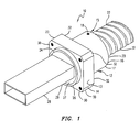
- FIGURE 1 there is shown an elliptical waveguide connector 10 having received therein, in secured structural mounting therewith, an elliptical waveguide 22.
- the illustrated elliptical waveguide connector 10 includes a waveguide connector housing 12 having at a first end 13 a generally rectangular mounting flange 14.
- the mounting flange 14 is adapted for mating engagement with, and securement to, a second waveguide mounting flange, as described in more detail below.
- the generally rectangular mounting flange 14 is constructed with a generally cylindrical boss 16 having a cylindrical outer surface 17 extending rearwardly therefrom to define a second end 15.
- the boss 16 is constructed of sufficient length to accommodate a generally elliptical waveguide receiving portion and a stepped transformer therein, neither of which are seen in this view, but which are described in more detail below. Also shown is a top solder port 18 formed through the cylindrical outer surface 17 and within the generally cylindrical boss 16 of the waveguide connector housing 12 to afford access to the elliptical waveguide 22 received within the elliptical waveguide receiving portion constructed therein, for securement of said elliptical waveguide 22 thereto.
- the elliptical waveguide connector 10 of this particular embodiment is shown connected to a rectangular waveguide mounting flange 23.
- the rectangular waveguide mounting flange 23 is constructed with a generally cylindrical boss 24 extending therefrom, the boss 24 having a generally rectangular waveguide receiving portion 26 formed therein.
- a generally rectangular waveguide 28 is shown mounted thereto.
- the generally rectangular waveguide 28 is received within the generally rectangular waveguide receiving portion 26 formed in the generally cylindrical boss 24 and secured therein by solder.
- a plurality of solder ports 29 are shown to be formed within a face 27 of the generally cylindrical boss 24. The solder ports 29 in the face 27 permit the introduction of solder around the rectangular waveguide 28 as heat is applied thereto.
- the rectangular waveguide 28 is securely mounted within the rectangular waveguide receiving portion 26 of the generally cylindrical boss 24.
- the rectangular waveguide 28 is securely positioned in abutting relationship against mating surfaces presented within the rectangular waveguide receiving portion 26, prior to soldering, for the necessary structural securement thereof and for the efficient operation-therewith.
- With proper alignment of the waveguide 28 against the above-referenced mating surface it is feasible to prevent molten solder from dripping into the waveguide or into the waveguide-receiving portion 26.
- Such an assembly error could have the deleterious effect of negative performance due to increased reflection losses and/or impedance mismatches.
- waveguide connecting flanges for the coupling of waveguide connectors is well established.
- the fabrication of the generally cylindrical boss 24 as a portion of such connecting flanges may be preferred in certain applications due to the fact that it is easier to machine a cylindrical region, with the use of a lathe or the like.
- a plurality of apertures 32 are thus formed in the mounting flange 14 of the waveguide connector housing 12 of the present invention, for mating coupling with the apertures 30, as discussed below.
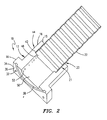
- FIGURE 2 there is shown an enlarged, perspective view of the connector 10 and waveguide 22 of FIG. 1, illustrating various aspects of the construction thereof.
- the plurality of apertures 32 are formed within the mounting flange 14 in the corners thereof and in registry with the apertures 30 of the flange 23 as shown in FIG. 1.
- a groove 34 is formed in a face 36 of the waveguide connector housing 12 to therein provide means for mounting an o-ring (not shown) and further defining a mating surface 38 for abutting engagement with a respective mating surface on the mounting flange 23 shown in FIG. 1.
- the O-ring mounting aspect is optional and is shown for purposes of illustration.
- the elliptical waveguide receiving portion 20 which comprises an elliptical cavity 21 constructed in the end 15 of the waveguide connector housing 12 and terminating in a shoulder 42 formed therein.
- the cavity 21 of the elliptical waveguide receiving portion 20 thus forms a sleeve 44 of substantially mating configuration with the elliptical waveguide 22 that is received therein.
- the sleeve 44 in this particular embodiment is sized to permit a slip fit interengagement between the elliptical waveguide 22 and the waveguide connector 10 having the housing 12 with an end 48 of the waveguide 22 abutting firmly against the shoulder 42 of the elliptical waveguide receiving portion 20.
- This abutting relationship is required for the use of molten solder, as referenced above. Due to the length of the cavity 21 defining the sleeve 44 between the shoulder 42 and the end 15 of the waveguide connector housing 12, the elliptical waveguide 22 may be securely mounted thereto. In the present embodiment, solder is then available for use in securing the elliptical waveguide 22 within the sleeve 44.
- This secured mounting is preferably effected without the need for flaring of the elliptical waveguide 22.
- the end 48 can be flared and the sleeve 44 dimensioned accordingly to accommodate the flaring of the end 48.
- an axial passageway 50 is formed within the housing 12.
- the passageway 50 is formed of sufficient length to provide an integrally formed inhomogeneous waveguide connector and transition for joining a rectangular waveguide to an elliptical waveguide as set forth above.
- the construction of the passageway 50, with side walls 52 and 53, including a stepped transformer formed therein, will be described in more detail below.
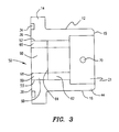
- FIGURE 3 there is shown an enlarged top plan, cross-sectional view of the waveguide connector housing 12 of FIG. 1, illustrating certain aspects of the construction thereof.
- the waveguide connector housing 12 of this particular embodiment is of unitary construction with the mounting flange 14 having the groove 34 formed therein around the face 38.
- the passageway 50 extends from the face 36 to the end 15, where a lower solder port 70 is formed in the elliptical cavity 21.
- the passageway 50 is also preferably formed in this embodiment by machining or the like, with the side walls 52 and 53 defining transition sections 60 and 62 axially aligned one with the other.
- the transition sections 60 and 62 shown herein are milled in the waveguide connector housing 12 and are separated by a shoulder portion 64.
- the transition sections 60 and 62 are specifically sized to form a waveguide stepped transformer for joining a rectangular waveguide to an elliptical waveguide.
- the method of construction of the transition sections 60 and 62 of this particular embodiment produces transition lines 66 and 68, which may be seen along the portion of passageway 50 forming the transition section 60.
- the transition lines 66 and 68 are formed when curved machined comers 67 and 69, respectively, intersect with planar sections of passageway 50 forming planar bottom surface 90.
- FIG. 4 there is shown an isolated perspective view of the waveguide connector 10 and the elliptical waveguide 22 mounted therein.
- the waveguide connector housing 12 of this particular embodiment may be seen to have the mounting flange 14 formed with the four apertures 32 positioned in the four comers thereof and adapted to be in registry with the apertures 30 of the flange 23 of FIG. 1.
- the passageway 50 providing the integrally formed stepped transformer is clearly shown, and the first transition section 60 of the transformer may be seen in conjunction with the transition lines 66 and 68 discussed above.
- the transition lines 66 and 68 define the changing shape of the passageway 50 in the transition section 60 between the planar bottom surface 90 and lower curved wall regions 67 and 69, respectively, of the passageway 50, the same defining the first transition section 60.
- the top solder port 18 is shown in the generally cylindrical boss 16. The top solder port 18, in conjunction with lower solder port 70 shown in FIG. 3, further facilitates the securement of the elliptical waveguide 22 within the sleeve 44 defined within the boss 16 by facilitating the application of molten solder within the sleeve 44.
- the construction of the elliptical waveguide connector 10 includes the provision of the sufficiently long, generally cylindrical boss 16 to afford sufficient length for both the stepped transformer and the secured mounting of the waveguide 22. Since the use of molten solder has been a proven mounting technique for rectangular waveguides, the ability to utilize such molten material with an elliptical waveguide is a marked advance over prior designs. By securely abutting the elliptical waveguide 22 in the sleeve 44 as described above, a reliable mounting configuration is provided in an assembly that can be easily fabricated at a relatively low cost. The connection between the elliptical waveguide 22 and the sleeve 44 as shown herein further accommodates the bending moments that can be created between a flexible waveguide and the connector secured thereto.
- the connector 10 of FIGS 1-4 may be easily and reliably secured to the elliptical waveguide 22 by insertion of the end 15 of the waveguide 22 into the sleeve 44.
- the end 15 of the waveguide 22 is positioned in abutting relationship with the shoulder 42 and molten solder is applied thereby via the solder ports 18 and 70 extending transversely through the waveguide connector housing 12.
- solder introduced through the solder ports 18 and 70, along with the introduction of heat, the solder (not shown) is allowed to flow and/or wick around the elliptical waveguide 22 to therein form a bond between the elliptical waveguide 22 and the sleeve 44 which, upon cooling, secures the engagement of the elliptical waveguide 22 to the elliptical waveguide connector 10.
- the design of the connector 10 thus permits solder to be used for elliptical waveguide mounting without the potentially deleterious effects thereof referenced above.
- the waveguide connector 100 of FIG. 5 includes a generally cylindrical housing 102 having a first end 104 formed with a generally rectangular waveguide receiving portion 106 formed therein.
- the generally rectangular waveguide receiving portion 106 is formed of a generally rectangular orifice 108 having side walls 110 terminating in a shoulder 112.
- a plurality of solder ports 114 are formed in opposite comers of the generally rectangular orifice 108 and a passageway 120 extends therefrom.
- the passageway 120 is constructed to form a stepped transformer of the type defined above as an integral portion thereof and as further illustrated below.
- a second, opposite end 130 of the housing 102 is constructed for receipt of a generally elliptical waveguide (not shown) as described above.
- a first solder port 132 is shown constructed within a top surface 134 of the housing 102. More specific aspects of the utilization of solder ports, as well as the construction of the housing 102, will be described in more detail below.
- the housing 102 will permit the connection of a generally rectangular waveguide to a generally elliptical waveguide without the utilization of waveguide flanges and/or the necessity of threaded fasteners therewith.
- the connection of the generally rectangular waveguide to the generally elliptical waveguide may be effected solely by the utilization of solder and the application of heat to firmly secure the respective waveguides within the connector 100, which may be of unitary construction.
- Other functional aspects of the connector 100 for example, the design and construction of the passageway 120 as an inhomogeneous waveguide connector, are essentially the same as that described above relative to the utilization of the connector 10 shown in FIG. 1.
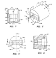
- FIG. 6 there is shown an end elevational view of the waveguide connector 100 of FIG. 5.
- the face 104 illustrated with the generally rectangular waveguide receiving portion 106 comprises the generally rectangular orifice 108 defining the passageway 120 formed through housing 102.
- the apertures 114 may be seen to be integral portions of the opposite comers of the generally rectangular orifice 108.
- FIG. 7 there is shown a top plan cross-sectional view of the housing 102 of FIG. 5 illustrating, in more detail, the passageway 120 formed therethrough and a lower solder port 140 formed therein.
- the solder port 140 is disposed in an elliptical waveguide receiving sleeve 150 extending inwardly from the end 130 of the housing 102.
- the sleeve 150 is constructed in the same manner as the sleeve 44 of the connector 10 described above.
- Sleeve 150 thus includes a generally elliptical waveguide receiving portion 152 having elliptical sidewalls 154 adapted for slip fit receipt and engagement of a generally elliptical waveguide therein.
- a shoulder 156 defines the innermost portion of the sleeve 150.
- the shoulder 156 is adapted for abutting engagement of a generally elliptical waveguide thereagainst in the manner described above relative to the shoulder 42 of the sleeve 44 of the connector 10.
- First and second transition sections, 160 and 162, respectively, are also formed within the passageway 120 connecting the sleeve 150 to the generally rectangular orifice 108 forming the generally rectangular waveguide receiving portion 106 of the end 104 of the housing 102.
- FIG. 8 there is shown a side elevational cross-sectional view of the housing 102 of FIG. 5 illustrating the passageway 120 formed therethrough and other aspects of the construction thereof.
- the top solder port 132 is shown oppositely disposed from the lower solder port 140 formed within the sleeve 150 of the housing 102.
- the solder ports 132 and 140 permit the access of solder to the region of the sleeve 150 for securement of an elliptical waveguide therein.
- the connector 100 of FIGS 5-8 may easily and reliably secured to the elliptical waveguide 22 by the insertion of an end portion of the waveguide 22 into the sleeve 150.
- the end of the waveguide 22 is positioned in abutting relationship with the shoulder 156 and molten solder is applied thereby via the solder ports 132 and 140 extending transversely through the cylindrical housing 102.
- the solder By the utilization of solder introduced through the solder ports 132 and 140 along with the introduction of heat, the solder (not shown) is allowed to flow and/or wick around the elliptical waveguide 22 (shown in FIGS 1-4) to therein form a bond between the elliptical waveguide 22 and the sleeve 150, which, upon cooling, secures the engagement of the elliptical waveguide 22 to the waveguide connector 100.
- Such mounting and securement may be performed "in the field” with essentially the same ease as the use of threaded fasteners, but with greater reliability.
- the insertion and secured mounting of a second, opposite waveguide may be effected with equal simplicity as described above.
- the second, opposite waveguide may be of any conventional shape, including, but not limited to, rectangular waveguides as shown herein.
Landscapes
- Waveguide Connection Structure (AREA)
- Waveguide Switches, Polarizers, And Phase Shifters (AREA)
- Waveguides (AREA)
Applications Claiming Priority (2)
| Application Number | Priority Date | Filing Date | Title |
|---|---|---|---|
| US09/924,645 US6583693B2 (en) | 2001-08-07 | 2001-08-07 | Method of and apparatus for connecting waveguides |
| US924645 | 2001-08-07 |
Publications (2)
| Publication Number | Publication Date |
|---|---|
| EP1289048A2 true EP1289048A2 (de) | 2003-03-05 |
| EP1289048A3 EP1289048A3 (de) | 2003-08-06 |
Family
ID=25450484
Family Applications (1)
| Application Number | Title | Priority Date | Filing Date |
|---|---|---|---|
| EP02017605A Withdrawn EP1289048A3 (de) | 2001-08-07 | 2002-08-05 | Verfahren und Gerät zur Verbindung von Hohlleitern |
Country Status (5)
| Country | Link |
|---|---|
| US (1) | US6583693B2 (de) |
| EP (1) | EP1289048A3 (de) |
| JP (1) | JP2003110313A (de) |
| BR (1) | BR0202959A (de) |
| CA (1) | CA2392792A1 (de) |
Cited By (4)
| Publication number | Priority date | Publication date | Assignee | Title |
|---|---|---|---|---|
| GB2518781A (en) * | 2012-05-16 | 2015-04-01 | Flexiguide Ltd | Waveguide assembly |
| CN112928414A (zh) * | 2021-01-27 | 2021-06-08 | 波达通信设备(广州)有限公司 | 波导传输装置及传输系统 |
| CN114976552A (zh) * | 2022-06-21 | 2022-08-30 | 西安金波科技有限责任公司 | 一种高性能四腔同轴波导转换器 |
| US12046793B2 (en) | 2019-12-24 | 2024-07-23 | Olympus Corporation | Connection structure of waveguide, waveguide connector, mode converter, and waveguide unit |
Families Citing this family (19)
| Publication number | Priority date | Publication date | Assignee | Title |
|---|---|---|---|---|
| SE518507C2 (sv) * | 2000-12-11 | 2002-10-15 | Allgon Ab | Vågledare och anslutningsdon för en sådan |
| US6448875B1 (en) * | 2001-03-07 | 2002-09-10 | Matthew J. Sciarrino | Waveguide interconnection system |
| JP2004343833A (ja) * | 2003-05-13 | 2004-12-02 | Toshiba Corp | モータ制御装置 |
| JP2005079878A (ja) * | 2003-08-29 | 2005-03-24 | Maspro Denkoh Corp | アンテナ |
| US7893789B2 (en) * | 2006-12-12 | 2011-02-22 | Andrew Llc | Waveguide transitions and method of forming components |
| US7791438B2 (en) * | 2007-06-07 | 2010-09-07 | Oml, Inc. | Millimeter and sub-millimeter wave waveguide interface having a junction of tight tolerance and a junction of lesser tolerance |
| KR101009615B1 (ko) * | 2008-06-20 | 2011-01-21 | 한국기초과학지원연구원 | 규격에 따른 도파관과 윈도우 접속 구조 |
| US8816791B2 (en) | 2010-09-28 | 2014-08-26 | Aviat U.S., Inc. | Systems and methods of a rectangular-to-circular waveguide transition |
| KR102447365B1 (ko) * | 2016-01-14 | 2022-09-23 | 엘에스전선 주식회사 | 도파관 어댑터 |
| JP6649110B2 (ja) * | 2016-02-16 | 2020-02-19 | 古野電気株式会社 | 可撓導波管、コネクタ、および電磁波伝送システム |
| RU2667324C1 (ru) * | 2016-12-27 | 2018-09-18 | федеральное государственное бюджетное образовательное учреждение высшего образования "Национальный исследовательский университет "МЭИ" (ФГБОУ ВО "НИУ "МЭИ") | Разъёмное соединение фланцев волноводов СВЧ трактов |
| PL232563B1 (pl) * | 2017-08-03 | 2019-06-28 | Inst Agrofizyki Im Bohdana Dobrzanskiego Polskiej Akademii Nauk | Złącze linii współosiowych lub falowodowych oraz sposób ich łączenia |
| CN107787109A (zh) * | 2017-11-21 | 2018-03-09 | 中国原子能科学研究院 | 传输波导与加速腔链的连接波导 |
| USD908641S1 (en) | 2017-11-30 | 2021-01-26 | Roos Instruments, Inc. | Blind mate waveguide flange |
| US10547113B2 (en) * | 2017-11-30 | 2020-01-28 | Roos Instruments, Inc. | Blind mate waveguide flange usable in chipset testing |
| CN114122644B (zh) * | 2020-08-31 | 2025-04-18 | 中兴通讯股份有限公司 | 一种波导接口结构 |
| WO2022079769A1 (ja) * | 2020-10-12 | 2022-04-21 | オリンパス株式会社 | 導波管の接続構造、導波管コネクタ、導波管ユニット、モード変換機、撮像装置、及び、内視鏡 |
| CN114986085B (zh) * | 2022-04-22 | 2024-03-01 | 成都欧拉微波元器件有限公司 | 扭波导加工方法 |
| CN116154441A (zh) * | 2023-03-08 | 2023-05-23 | 电子科技大学长三角研究院(湖州) | 一种波导转换器、控制方法及应用 |
Family Cites Families (21)
| Publication number | Priority date | Publication date | Assignee | Title |
|---|---|---|---|---|
| GB844373A (en) * | 1956-08-31 | 1960-08-10 | Ici Ltd | Wave-guide coupling |
| US2975380A (en) * | 1957-09-30 | 1961-03-14 | Raytheon Co | Waveguide transducer |
| US3374450A (en) * | 1965-11-17 | 1968-03-19 | Litton Prec Products Inc | Waveguide flange and coupling assembly |
| FR1536396A (fr) * | 1967-07-05 | 1968-08-16 | Pièce intermédiaire, en particulier bride, entre guides d'ondes rigide et flexible | |
| SE346486B (de) * | 1968-12-23 | 1972-07-10 | Graenges Essem Ab | |
| JPS5118673Y1 (de) * | 1970-07-10 | 1976-05-18 | ||
| GB1393391A (en) | 1971-04-19 | 1975-05-07 | Spinner G | End fitting for hf transmission lines |
| CA995711A (en) * | 1972-05-26 | 1976-08-24 | Licentia Patent-Verwaltungs-Gmbh | Pipe flange |
| US3818383A (en) | 1973-02-27 | 1974-06-18 | Andrew Corp | Elliptical-to-rectangular waveguide transition |
| US3928825A (en) | 1973-05-04 | 1975-12-23 | Licentia Gmbh | Waveguide transition piece with low reflection |
| GB1501405A (en) | 1974-06-01 | 1978-02-15 | Licentia Gmbh | Arrangement with a hollow waveguide section |
| US4447811A (en) | 1981-10-26 | 1984-05-08 | The United States Of America As Represented By The Secretary Of The Navy | Dielectric loaded horn antennas having improved radiation characteristics |
| US4642585A (en) | 1985-01-30 | 1987-02-10 | Andrew Corporation | Superelliptical waveguide connection |
| DE3631981C1 (de) * | 1986-09-19 | 1987-12-17 | Georg Dr-Ing Spinner | Transformationsteil zum Verbinden von zwei Hohlleitern unterschiedlicher Querschnittsformen |
| US4932673A (en) * | 1988-02-01 | 1990-06-12 | Hughes Aircraft Company | Emi suppression gasket for millimeter waveguides |
| FR2660803A1 (fr) * | 1990-04-06 | 1991-10-11 | Thomson Csf | Dispositif et piece de raccordement pour guides d'ondes hyperfrequence. |
| GB9103067D0 (en) * | 1991-02-13 | 1991-03-27 | Quasar Microwave Tech | Elliptical waveguides |
| US5148593A (en) * | 1991-08-01 | 1992-09-22 | W. L. Gore & Associates, Inc. | Method for jointing a dielectric waveguide |
| IT1252387B (it) * | 1991-11-12 | 1995-06-12 | Telettra S P A Ora Alcatel Ita | Flange e corpi per componenti in guida d'onda a microonde |
| DE19615854C1 (de) | 1996-04-20 | 1997-11-20 | Alcatel Kabel Ag | Verfahren zur Herstellung einer Kupplung für das Verbinden zweier elektromagnetischer Hohlleiter |
| US6140893A (en) * | 1999-04-26 | 2000-10-31 | Sciarrino; Anthony J. | Waveguide interconnection system |
-
2001
- 2001-08-07 US US09/924,645 patent/US6583693B2/en not_active Expired - Lifetime
-
2002
- 2002-07-08 CA CA002392792A patent/CA2392792A1/en not_active Abandoned
- 2002-07-29 BR BR0202959-6A patent/BR0202959A/pt not_active Application Discontinuation
- 2002-07-30 JP JP2002220619A patent/JP2003110313A/ja not_active Withdrawn
- 2002-08-05 EP EP02017605A patent/EP1289048A3/de not_active Withdrawn
Cited By (6)
| Publication number | Priority date | Publication date | Assignee | Title |
|---|---|---|---|---|
| GB2518781A (en) * | 2012-05-16 | 2015-04-01 | Flexiguide Ltd | Waveguide assembly |
| GB2518781B (en) * | 2012-05-16 | 2016-03-09 | Flexiguide Ltd | Waveguide assembly |
| US12046793B2 (en) | 2019-12-24 | 2024-07-23 | Olympus Corporation | Connection structure of waveguide, waveguide connector, mode converter, and waveguide unit |
| CN112928414A (zh) * | 2021-01-27 | 2021-06-08 | 波达通信设备(广州)有限公司 | 波导传输装置及传输系统 |
| CN112928414B (zh) * | 2021-01-27 | 2022-02-11 | 波达通信设备(广州)有限公司 | 波导传输装置及传输系统 |
| CN114976552A (zh) * | 2022-06-21 | 2022-08-30 | 西安金波科技有限责任公司 | 一种高性能四腔同轴波导转换器 |
Also Published As
| Publication number | Publication date |
|---|---|
| CA2392792A1 (en) | 2003-02-07 |
| BR0202959A (pt) | 2003-06-03 |
| JP2003110313A (ja) | 2003-04-11 |
| US6583693B2 (en) | 2003-06-24 |
| US20030030503A1 (en) | 2003-02-13 |
| EP1289048A3 (de) | 2003-08-06 |
Similar Documents
| Publication | Publication Date | Title |
|---|---|---|
| US6583693B2 (en) | Method of and apparatus for connecting waveguides | |
| AU2002356968B2 (en) | Electromagnetic coupling | |
| CN100524953C (zh) | 具有多条传输线路用的共用接地触点的无焊料印刷电路板边缘连接器 | |
| US8013687B2 (en) | Ortho-mode transducer with TEM probe for coaxial waveguide | |
| EP1331686B1 (de) | Hohlleiteradapteranordnung und zugehöriges Verfahren | |
| KR101018980B1 (ko) | 전기 접점부 | |
| US20050285702A1 (en) | Universal waveguide interface adaptor | |
| CN1327279A (zh) | 具有阻抗匹配片的rf连接器 | |
| US4366453A (en) | Orthogonal mode transducer having interface plates at the junction of the waveguides | |
| US5347244A (en) | Broadband directional coupler using cables | |
| CN109524753A (zh) | 波导同轴微带转换电路 | |
| EP0172570A2 (de) | Elliptischer Wellenleiter oder Hornstrahler mit Rillenstruktur | |
| CN216015642U (zh) | 一种无法兰波导连接结构 | |
| JP3513039B2 (ja) | 同軸導波管変換器 | |
| CN211455965U (zh) | 一种适用于不同尺寸射频同轴电缆之间的对接结构 | |
| US6902422B1 (en) | Cable connector | |
| JPH08186410A (ja) | 同軸導波管変換器 | |
| CA2086060C (en) | Broadband directional coupler using cables | |
| US12512577B1 (en) | Magic tee waveguide structure with triangular impedance matching element | |
| US5692927A (en) | Connection arrangement | |
| KR20010036428A (ko) | 딥 브레이징을 위한 도파관 구조 | |
| SU1716581A1 (ru) | Циркул тор | |
| WO2025002028A1 (zh) | 天线装置及通信设备 | |
| CN120432918A (zh) | 直角高频连接器及其制作方法 | |
| TW202422970A (zh) | 多埠連接器 |
Legal Events
| Date | Code | Title | Description |
|---|---|---|---|
| PUAI | Public reference made under article 153(3) epc to a published international application that has entered the european phase |
Free format text: ORIGINAL CODE: 0009012 |
|
| AK | Designated contracting states |
Kind code of ref document: A2 Designated state(s): AT BE BG CH CY CZ DE DK EE ES FI FR GB GR IE IT LI LU MC NL PT SE SK TR Designated state(s): AT BE BG CH CY CZ DE DK EE ES FI FR GB GR IE IT LI LU MC NL PT SE SK TR |
|
| AX | Request for extension of the european patent |
Extension state: AL LT LV MK RO SI |
|
| PUAL | Search report despatched |
Free format text: ORIGINAL CODE: 0009013 |
|
| AK | Designated contracting states |
Designated state(s): AT BE BG CH CY CZ DE DK EE ES FI FR GB GR IE IT LI LU MC NL PT SE SK TR |
|
| AX | Request for extension of the european patent |
Extension state: AL LT LV MK RO SI |
|
| RIC1 | Information provided on ipc code assigned before grant |
Ipc: 7H 01P 1/04 B Ipc: 7H 01P 5/08 A |
|
| AKX | Designation fees paid | ||
| REG | Reference to a national code |
Ref country code: DE Ref legal event code: 8566 |
|
| STAA | Information on the status of an ep patent application or granted ep patent |
Free format text: STATUS: THE APPLICATION IS DEEMED TO BE WITHDRAWN |
|
| 18D | Application deemed to be withdrawn |
Effective date: 20040207 |