EP1289015B1 - Multicolor light emission apparatus and manufacturing method thereof - Google Patents
Multicolor light emission apparatus and manufacturing method thereof Download PDFInfo
- Publication number
- EP1289015B1 EP1289015B1 EP02018281A EP02018281A EP1289015B1 EP 1289015 B1 EP1289015 B1 EP 1289015B1 EP 02018281 A EP02018281 A EP 02018281A EP 02018281 A EP02018281 A EP 02018281A EP 1289015 B1 EP1289015 B1 EP 1289015B1
- Authority
- EP
- European Patent Office
- Prior art keywords
- layer
- light emission
- compound
- organic
- transporting layer
- Prior art date
- Legal status (The legal status is an assumption and is not a legal conclusion. Google has not performed a legal analysis and makes no representation as to the accuracy of the status listed.)
- Expired - Lifetime
Links
Images

Classifications
-
- H—ELECTRICITY
- H05—ELECTRIC TECHNIQUES NOT OTHERWISE PROVIDED FOR
- H05B—ELECTRIC HEATING; ELECTRIC LIGHT SOURCES NOT OTHERWISE PROVIDED FOR; CIRCUIT ARRANGEMENTS FOR ELECTRIC LIGHT SOURCES, IN GENERAL
- H05B33/00—Electroluminescent light sources
- H05B33/12—Light sources with substantially two-dimensional radiating surfaces
- H05B33/14—Light sources with substantially two-dimensional radiating surfaces characterised by the chemical or physical composition or the arrangement of the electroluminescent material, or by the simultaneous addition of the electroluminescent material in or onto the light source
-
- H—ELECTRICITY
- H10—SEMICONDUCTOR DEVICES; ELECTRIC SOLID-STATE DEVICES NOT OTHERWISE PROVIDED FOR
- H10K—ORGANIC ELECTRIC SOLID-STATE DEVICES
- H10K59/00—Integrated devices, or assemblies of multiple devices, comprising at least one organic light-emitting element covered by group H10K50/00
- H10K59/30—Devices specially adapted for multicolour light emission
- H10K59/35—Devices specially adapted for multicolour light emission comprising red-green-blue [RGB] subpixels
-
- H—ELECTRICITY
- H10—SEMICONDUCTOR DEVICES; ELECTRIC SOLID-STATE DEVICES NOT OTHERWISE PROVIDED FOR
- H10K—ORGANIC ELECTRIC SOLID-STATE DEVICES
- H10K85/00—Organic materials used in the body or electrodes of devices covered by this subclass
- H10K85/60—Organic compounds having low molecular weight
- H10K85/615—Polycyclic condensed aromatic hydrocarbons, e.g. anthracene
- H10K85/626—Polycyclic condensed aromatic hydrocarbons, e.g. anthracene containing more than one polycyclic condensed aromatic rings, e.g. bis-anthracene
-
- H—ELECTRICITY
- H10—SEMICONDUCTOR DEVICES; ELECTRIC SOLID-STATE DEVICES NOT OTHERWISE PROVIDED FOR
- H10K—ORGANIC ELECTRIC SOLID-STATE DEVICES
- H10K85/00—Organic materials used in the body or electrodes of devices covered by this subclass
- H10K85/60—Organic compounds having low molecular weight
- H10K85/631—Amine compounds having at least two aryl rest on at least one amine-nitrogen atom, e.g. triphenylamine
- H10K85/633—Amine compounds having at least two aryl rest on at least one amine-nitrogen atom, e.g. triphenylamine comprising polycyclic condensed aromatic hydrocarbons as substituents on the nitrogen atom
-
- H—ELECTRICITY
- H10—SEMICONDUCTOR DEVICES; ELECTRIC SOLID-STATE DEVICES NOT OTHERWISE PROVIDED FOR
- H10K—ORGANIC ELECTRIC SOLID-STATE DEVICES
- H10K85/00—Organic materials used in the body or electrodes of devices covered by this subclass
- H10K85/60—Organic compounds having low molecular weight
- H10K85/649—Aromatic compounds comprising a hetero atom
- H10K85/657—Polycyclic condensed heteroaromatic hydrocarbons
-
- H—ELECTRICITY
- H10—SEMICONDUCTOR DEVICES; ELECTRIC SOLID-STATE DEVICES NOT OTHERWISE PROVIDED FOR
- H10K—ORGANIC ELECTRIC SOLID-STATE DEVICES
- H10K50/00—Organic light-emitting devices
- H10K50/10—OLEDs or polymer light-emitting diodes [PLED]
- H10K50/11—OLEDs or polymer light-emitting diodes [PLED] characterised by the electroluminescent [EL] layers
- H10K50/125—OLEDs or polymer light-emitting diodes [PLED] characterised by the electroluminescent [EL] layers specially adapted for multicolour light emission, e.g. for emitting white light
-
- H—ELECTRICITY
- H10—SEMICONDUCTOR DEVICES; ELECTRIC SOLID-STATE DEVICES NOT OTHERWISE PROVIDED FOR
- H10K—ORGANIC ELECTRIC SOLID-STATE DEVICES
- H10K85/00—Organic materials used in the body or electrodes of devices covered by this subclass
- H10K85/30—Coordination compounds
- H10K85/321—Metal complexes comprising a group IIIA element, e.g. Tris (8-hydroxyquinoline) gallium [Gaq3]
- H10K85/324—Metal complexes comprising a group IIIA element, e.g. Tris (8-hydroxyquinoline) gallium [Gaq3] comprising aluminium, e.g. Alq3
-
- H—ELECTRICITY
- H10—SEMICONDUCTOR DEVICES; ELECTRIC SOLID-STATE DEVICES NOT OTHERWISE PROVIDED FOR
- H10K—ORGANIC ELECTRIC SOLID-STATE DEVICES
- H10K85/00—Organic materials used in the body or electrodes of devices covered by this subclass
- H10K85/30—Coordination compounds
- H10K85/341—Transition metal complexes, e.g. Ru(II)polypyridine complexes
- H10K85/342—Transition metal complexes, e.g. Ru(II)polypyridine complexes comprising iridium
-
- H—ELECTRICITY
- H10—SEMICONDUCTOR DEVICES; ELECTRIC SOLID-STATE DEVICES NOT OTHERWISE PROVIDED FOR
- H10K—ORGANIC ELECTRIC SOLID-STATE DEVICES
- H10K85/00—Organic materials used in the body or electrodes of devices covered by this subclass
- H10K85/60—Organic compounds having low molecular weight
- H10K85/631—Amine compounds having at least two aryl rest on at least one amine-nitrogen atom, e.g. triphenylamine
- H10K85/636—Amine compounds having at least two aryl rest on at least one amine-nitrogen atom, e.g. triphenylamine comprising heteroaromatic hydrocarbons as substituents on the nitrogen atom
-
- H—ELECTRICITY
- H10—SEMICONDUCTOR DEVICES; ELECTRIC SOLID-STATE DEVICES NOT OTHERWISE PROVIDED FOR
- H10K—ORGANIC ELECTRIC SOLID-STATE DEVICES
- H10K85/00—Organic materials used in the body or electrodes of devices covered by this subclass
- H10K85/60—Organic compounds having low molecular weight
- H10K85/649—Aromatic compounds comprising a hetero atom
- H10K85/653—Aromatic compounds comprising a hetero atom comprising only oxygen as heteroatom
-
- H—ELECTRICITY
- H10—SEMICONDUCTOR DEVICES; ELECTRIC SOLID-STATE DEVICES NOT OTHERWISE PROVIDED FOR
- H10K—ORGANIC ELECTRIC SOLID-STATE DEVICES
- H10K85/00—Organic materials used in the body or electrodes of devices covered by this subclass
- H10K85/60—Organic compounds having low molecular weight
- H10K85/649—Aromatic compounds comprising a hetero atom
- H10K85/654—Aromatic compounds comprising a hetero atom comprising only nitrogen as heteroatom
-
- H—ELECTRICITY
- H10—SEMICONDUCTOR DEVICES; ELECTRIC SOLID-STATE DEVICES NOT OTHERWISE PROVIDED FOR
- H10K—ORGANIC ELECTRIC SOLID-STATE DEVICES
- H10K85/00—Organic materials used in the body or electrodes of devices covered by this subclass
- H10K85/60—Organic compounds having low molecular weight
- H10K85/649—Aromatic compounds comprising a hetero atom
- H10K85/656—Aromatic compounds comprising a hetero atom comprising two or more different heteroatoms per ring
- H10K85/6565—Oxadiazole compounds
-
- Y—GENERAL TAGGING OF NEW TECHNOLOGICAL DEVELOPMENTS; GENERAL TAGGING OF CROSS-SECTIONAL TECHNOLOGIES SPANNING OVER SEVERAL SECTIONS OF THE IPC; TECHNICAL SUBJECTS COVERED BY FORMER USPC CROSS-REFERENCE ART COLLECTIONS [XRACs] AND DIGESTS
- Y10—TECHNICAL SUBJECTS COVERED BY FORMER USPC
- Y10T—TECHNICAL SUBJECTS COVERED BY FORMER US CLASSIFICATION
- Y10T428/00—Stock material or miscellaneous articles
- Y10T428/12—All metal or with adjacent metals
- Y10T428/12451—Macroscopically anomalous interface between layers
Definitions
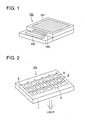
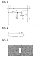
- An organic EL element 10 has plural organic layers and two opposed electrodes between which the organic layers are provided. When current is applied across the plural organic layers through the electrode, light is emitted from a predetermined organic layer according to the amount of the current.
- the adjacent layer which will be described later, can be broadly classified into two, that is, a hole transporting layer and an electron transporting layer due to its function. Further, the adjacent layer can be narrowly classified into a hole injecting layer, a hole transporting layer, an electron blocking layer, an electron injecting layer, an electron transporting layer, and a hole blocking layer due to its function.
- the hole transporting light emission layer or electron transporting light emission layer is the light emission layer in the invention, and a layer adjacent to the light emission layer are an adjacent layer.
- the electron blocking layer is an hole transporting layer in a broad sense, and is comprised of material having an ability of transporting holes but an extremely poor ability of electrons, which can increase a recombination probability of electrons and holes by transporting holes and blocking electrons.
- the present invention has been attained employing, as the host, compound having a maximum emission (fluorescence) wavelength in the wavelength regions shorter than the blue wavelength regions, and a maximum emission (fluorescence) wavelength not longer than 415 nm, and employing the same host in the plural organic EL elements. Further, use of compounds having a maximum emission (fluorescence) wavelength not longer than 415 nm as the hole transporting compound or the electron transporting compound has made it possible to employ the same compound in the hole transporting layer or the electron transporting layer of each of the plural organic EL elements. Employing the same compound in the hole transporting layer or the electron transporting layer of each of the plural organic EL elements means that a multicolor light emission apparatus can be manufactured simultaneously forming the same layers as the common layer, regardless of the kinds of the organic EL elements.
- Examples of the dopant compound will be listed below, but are not limited thereto.
- the ordinary ⁇ conjugated fluorescent or phosphorescent compound in which the maximum emission wavelength is adjusted to not longer than 415 nm, has a ⁇ - ⁇ absorption in the wavelength regions of not longer than 420 nm, and can carry out a dopant emission of energy transfer type.
- the fluorescence of not longer than 415 nm provides a wide energy gap (ionization potential-electron affinity, HOMO-LUMO), and advantageously works in the carrier trap type.
- the hole transporting layer comprises a compound having a hole transporting ability, and in a broad sense refers to a hole injecting layer or an electron blocking layer.
- the hole transporting layer can be provided as a single layer or plural layers.
- a polymer in which the compound mentioned above is introduced in the polymer chain or a polymer having the material as the polymer main chain can be also used.
- a hue improving filter such as a color filter may be used in combination.
- the multicolor light emission apparatus of the invention comprises at least two organic EL elements each having a different maximum emission wavelength. Preferable examples in the preparation of the organic EL element will be described below.
- a multicolor light emission apparatus sample No. 8 was prepared in the same manner as in Comparative Example 1, except that only the host compound in the red light emission layer was changed from Bebq to Alq3.
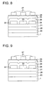
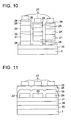
- the shadow mask was removed, and BC was deposited on the entire surface of the resulting layer to obtain a hole blocking layer 29 with a thickness of 10 nm. Further, Alq3 was deposited on the entire surface of the resulting layer to obtain an electron transporting layer 25 with a thickness of 30 nm, and LiF was deposited on the entire surface of the resulting layer to obtain a 0.5 nm thick LiF layer.
- a shadow mask with openings for cathode patterning was prepared.
- the shadow mask had reinforcing materials on one side thereof to prevent deformation of the openings, and had the structure in which a space is formed between the substrate and the shadow mask with the reinforcing materials.
- the shadow mask had a size of 120 mm x 84 mm, and a thickness of 150 ⁇ m.
- the shadow mask had 200 openings in the stripe form with a length of 100 mm and a width of 200 ⁇ m which were provided at a pitch of 300 ⁇ m.
- the shadow mask had, on the masked portions, reinforcing materials with a width of 40 mm and a thickness of 35 ⁇ m, which was of regular hexagon-shaped mesh structure with a distance between the opposite sides of 20 ⁇ m.
- the space distance was 150 ⁇ m, equal to the thickness of the shadow mask.
- the shadow mask was fixed with a stainless steel frame.
Applications Claiming Priority (2)
| Application Number | Priority Date | Filing Date | Title |
|---|---|---|---|
| JP2001257720 | 2001-08-28 | ||
| JP2001257720 | 2001-08-28 |
Publications (3)
| Publication Number | Publication Date |
|---|---|
| EP1289015A2 EP1289015A2 (en) | 2003-03-05 |
| EP1289015A3 EP1289015A3 (en) | 2007-04-25 |
| EP1289015B1 true EP1289015B1 (en) | 2012-05-23 |
Family
ID=19085340
Family Applications (1)
| Application Number | Title | Priority Date | Filing Date |
|---|---|---|---|
| EP02018281A Expired - Lifetime EP1289015B1 (en) | 2001-08-28 | 2002-08-22 | Multicolor light emission apparatus and manufacturing method thereof |
Country Status (4)
Families Citing this family (50)
| Publication number | Priority date | Publication date | Assignee | Title |
|---|---|---|---|---|
| US20040004433A1 (en) * | 2002-06-26 | 2004-01-08 | 3M Innovative Properties Company | Buffer layers for organic electroluminescent devices and methods of manufacture and use |
| US7368659B2 (en) * | 2002-11-26 | 2008-05-06 | General Electric Company | Electrodes mitigating effects of defects in organic electronic devices |
| EP1464691B1 (en) * | 2003-03-26 | 2013-10-02 | Konica Minolta Holdings, Inc. | Organic electroluminescent element, illuminator, and display |
| CN100483779C (zh) * | 2003-05-29 | 2009-04-29 | 新日铁化学株式会社 | 有机电致发光元件 |
| JP2005038849A (ja) * | 2003-07-01 | 2005-02-10 | Semiconductor Energy Lab Co Ltd | 発光装置 |
| US20050008052A1 (en) * | 2003-07-01 | 2005-01-13 | Ryoji Nomura | Light-emitting device |
| JP4396163B2 (ja) * | 2003-07-08 | 2010-01-13 | 株式会社デンソー | 有機el素子 |
| DE10333232A1 (de) * | 2003-07-21 | 2007-10-11 | Merck Patent Gmbh | Organisches Elektrolumineszenzelement |
| US20050058853A1 (en) * | 2003-09-15 | 2005-03-17 | Eastman Kodak Company | Green organic light-emitting diodes |
| KR100543003B1 (ko) * | 2003-09-15 | 2006-01-20 | 삼성에스디아이 주식회사 | 풀칼라 유기 전계 발광 소자 및 그의 제조 방법 |
| JP2005093573A (ja) * | 2003-09-16 | 2005-04-07 | Ricoh Co Ltd | 有機半導体レーザ |
| US7935432B2 (en) | 2003-09-19 | 2011-05-03 | Fujifilm Corporation | Organic electroluminescent device |
| KR20050050487A (ko) * | 2003-11-25 | 2005-05-31 | 삼성에스디아이 주식회사 | 풀칼라 유기 전계 발광 소자 |
| KR100560790B1 (ko) | 2003-11-25 | 2006-03-13 | 삼성에스디아이 주식회사 | 고온 특성이 우수한 유기 전계 발광 표시 장치 |
| KR100659530B1 (ko) | 2003-11-26 | 2006-12-19 | 삼성에스디아이 주식회사 | 풀칼라 유기전계발광소자 |
| CN1890255B (zh) | 2003-12-02 | 2010-06-09 | 株式会社半导体能源研究所 | 有机金属络合物以及使用其的发光元件 |
| US7090930B2 (en) | 2003-12-05 | 2006-08-15 | Eastman Kodak Company | Organic element for electroluminescent devices |
| TWI230026B (en) * | 2003-12-31 | 2005-03-21 | Ritdisplay Corp | Organic electroluminescent material and organic electroluminescent device by using the same |
| KR100787425B1 (ko) * | 2004-11-29 | 2007-12-26 | 삼성에스디아이 주식회사 | 페닐카바졸계 화합물 및 이를 이용한 유기 전계 발광 소자 |
| US8188315B2 (en) | 2004-04-02 | 2012-05-29 | Samsung Mobile Display Co., Ltd. | Organic light emitting device and flat panel display device comprising the same |
| JP4912618B2 (ja) * | 2004-05-20 | 2012-04-11 | 株式会社半導体エネルギー研究所 | 発光素子、発光装置および照明器具 |
| EP1749424B1 (en) * | 2004-05-20 | 2011-10-19 | Semiconductor Energy Laboratory Co., Ltd. | Light emitting element and light emitting device |
| US7854998B2 (en) * | 2004-05-31 | 2010-12-21 | Kabushiki Kaisha Toyota Jidoshokki | Organic EL devices |
| JP5076501B2 (ja) * | 2004-07-16 | 2012-11-21 | コニカミノルタホールディングス株式会社 | 白色有機エレクトロルミネッセンス素子、画像表示素子および照明装置 |
| US20060066220A1 (en) * | 2004-09-27 | 2006-03-30 | Choong Vi-En | Reduction or elimination of color change with viewing angle for microcavity devices |
| US7803468B2 (en) * | 2004-09-29 | 2010-09-28 | Fujifilm Corporation | Organic electroluminescent element |
| KR100759548B1 (ko) * | 2004-10-15 | 2007-09-18 | 삼성에스디아이 주식회사 | 유기 전계 발광 소자 |
| US8021765B2 (en) | 2004-11-29 | 2011-09-20 | Samsung Mobile Display Co., Ltd. | Phenylcarbazole-based compound and organic electroluminescent device employing the same |
| WO2006062144A1 (en) * | 2004-12-07 | 2006-06-15 | Semiconductor Energy Laboratory Co., Ltd. | Organometallic complex, and light-emitting element and light-emittng device using the same |
| GB0428445D0 (en) | 2004-12-29 | 2005-02-02 | Cambridge Display Tech Ltd | Blue-shifted triarylamine polymer |
| US20070003785A1 (en) * | 2005-06-30 | 2007-01-04 | Eastman Kodak Company | Electroluminescent devices containing benzidine derivatives |
| JP4770699B2 (ja) * | 2005-12-16 | 2011-09-14 | ソニー株式会社 | 表示素子 |
| JP2007257897A (ja) * | 2006-03-20 | 2007-10-04 | Seiko Epson Corp | 発光素子の製造方法、発光装置の製造方法および電子機器の製造方法 |
| JP2007265763A (ja) * | 2006-03-28 | 2007-10-11 | Canon Inc | フルカラー有機elパネル |
| JP2007266160A (ja) * | 2006-03-28 | 2007-10-11 | Canon Inc | 有機発光素子アレイ |
| KR100756865B1 (ko) * | 2006-04-06 | 2007-09-07 | 비오이 하이디스 테크놀로지 주식회사 | 픽셀별로 상이한 두께의 유기 발광층을 갖는 유기 전계발광 표시소자 및 그 제조방법 |
| JP2008027722A (ja) * | 2006-07-21 | 2008-02-07 | Sony Corp | 表示装置および表示装置の製造方法 |
| KR100841363B1 (ko) * | 2006-11-22 | 2008-06-26 | 삼성에스디아이 주식회사 | 유기전계발광표시장치 및 그의 제조방법 |
| WO2008120714A1 (ja) * | 2007-03-29 | 2008-10-09 | Dai Nippon Printing Co., Ltd. | 有機エレクトロルミネッセンス素子及びその製造方法 |
| KR100858824B1 (ko) * | 2007-05-31 | 2008-09-17 | 삼성에스디아이 주식회사 | 유기 발광 소자 및 이의 제조 방법 |
| KR102115154B1 (ko) | 2008-05-16 | 2020-05-26 | 가부시키가이샤 한도오따이 에네루기 켄큐쇼 | 트리아릴아민 유도체, 발광 물질, 발광 소자, 발광 장치 및 전자 기기 |
| JP5618495B2 (ja) * | 2008-05-16 | 2014-11-05 | キヤノン株式会社 | 有機発光素子 |
| JP2010114428A (ja) * | 2008-10-10 | 2010-05-20 | Canon Inc | 有機el表示装置 |
| JP5676867B2 (ja) * | 2009-09-29 | 2015-02-25 | 住友化学株式会社 | 有機エレクトロルミネッセンス素子 |
| WO2011071169A1 (ja) * | 2009-12-11 | 2011-06-16 | 三菱化学株式会社 | 有機電界発光素子、有機el表示装置及び有機el照明 |
| KR102214317B1 (ko) | 2013-06-14 | 2021-02-08 | 가부시키가이샤 한도오따이 에네루기 켄큐쇼 | 유기 금속 이리듐 착체, 발광 소자, 발광 장치, 및 조명 장치 |
| JP6307993B2 (ja) | 2014-04-07 | 2018-04-11 | コニカミノルタ株式会社 | 有機エレクトロルミネッセンス素子、及び、電子デバイス |
| JP6888943B2 (ja) | 2016-11-17 | 2021-06-18 | 株式会社ジャパンディスプレイ | 有機エレクトロルミネッセンス表示装置 |
| US10254195B1 (en) | 2016-11-28 | 2019-04-09 | Amazon Technologies, Inc. | Wind tunnel for aerial vehicle certification |
| KR102192216B1 (ko) | 2017-12-26 | 2020-12-16 | 주식회사 엘지화학 | 아민계 화합물 및 이를 포함하는 유기 발광 소자 |
Family Cites Families (13)
| Publication number | Priority date | Publication date | Assignee | Title |
|---|---|---|---|---|
| US5294870A (en) * | 1991-12-30 | 1994-03-15 | Eastman Kodak Company | Organic electroluminescent multicolor image display device |
| US5294869A (en) * | 1991-12-30 | 1994-03-15 | Eastman Kodak Company | Organic electroluminescent multicolor image display device |
| JP3849066B2 (ja) * | 1996-05-15 | 2006-11-22 | ケミプロ化成株式会社 | マルチカラー有機el素子、その製法およびそれを用いたディスプレイ |
| KR100471523B1 (ko) * | 1996-05-15 | 2005-09-02 | 케미푸로 가세 가부시키가이샤 | 멀티칼라유기이엘소자,그제법및그것을사용한디스플레이 |
| JP2000082582A (ja) | 1998-06-30 | 2000-03-21 | Toray Ind Inc | 有機elディスプレイの製造方法 |
| US6097147A (en) * | 1998-09-14 | 2000-08-01 | The Trustees Of Princeton University | Structure for high efficiency electroluminescent device |
| US6166489A (en) * | 1998-09-15 | 2000-12-26 | The Trustees Of Princeton University | Light emitting device using dual light emitting stacks to achieve full-color emission |
| US6048573A (en) * | 1998-11-13 | 2000-04-11 | Eastman Kodak Company | Method of making an organic light-emitting device |
| JP2000228284A (ja) * | 1998-12-01 | 2000-08-15 | Sanyo Electric Co Ltd | カラーel表示装置 |
| US6066357A (en) * | 1998-12-21 | 2000-05-23 | Eastman Kodak Company | Methods of making a full-color organic light-emitting display |
| US6278236B1 (en) * | 1999-09-02 | 2001-08-21 | Eastman Kodak Company | Organic electroluminescent devices with electron-injecting layer having aluminum and alkali halide |
| JP2001319781A (ja) * | 2000-05-02 | 2001-11-16 | Fuji Photo Film Co Ltd | 有機発光素子材料の選択方法及びその材料を用いた有機発光素子 |
| US6606110B2 (en) * | 2000-12-27 | 2003-08-12 | Polaroid Corporation | Integral organic light emitting diode printhead |
-
2002
- 2002-08-22 JP JP2002241871A patent/JP4281308B2/ja not_active Expired - Fee Related
- 2002-08-22 EP EP02018281A patent/EP1289015B1/en not_active Expired - Lifetime
- 2002-08-22 US US10/225,859 patent/US6949878B2/en not_active Expired - Lifetime
- 2002-08-24 KR KR1020020050284A patent/KR100886976B1/ko active IP Right Grant
Also Published As
| Publication number | Publication date |
|---|---|
| JP2003151769A (ja) | 2003-05-23 |
| KR100886976B1 (ko) | 2009-03-04 |
| KR20030019897A (ko) | 2003-03-07 |
| US6949878B2 (en) | 2005-09-27 |
| US20030076032A1 (en) | 2003-04-24 |
| JP4281308B2 (ja) | 2009-06-17 |
| EP1289015A2 (en) | 2003-03-05 |
| EP1289015A3 (en) | 2007-04-25 |
Similar Documents
| Publication | Publication Date | Title |
|---|---|---|
| EP1289015B1 (en) | Multicolor light emission apparatus and manufacturing method thereof | |
| US6750608B2 (en) | Organic electroluminescence element and display | |
| JP4427947B2 (ja) | 有機エレクトロルミネッセンス素子及び表示装置 | |
| EP2762546B1 (en) | Organic electroluminescent element, and display and illuminator | |
| JP4288895B2 (ja) | 有機エレクトロルミネッセンスの製造方法 | |
| EP1786242B1 (en) | Organic electroluminescence device, display apparatus and lighting apparatus | |
| KR100915271B1 (ko) | 유기 전계발광 소자 및 표시 장치 | |
| JP3969132B2 (ja) | 有機エレクトロルミネッセンス素子及びそれを用いた表示装置 | |
| KR100751463B1 (ko) | 유기 전계 발광 소자 | |
| KR100751464B1 (ko) | 유기 전계 발광 소자 | |
| US7759855B2 (en) | Organic electroluminescent element and display employing the same | |
| JP2004178896A (ja) | 有機エレクトロルミネッセンス素子及び表示装置 | |
| EP0960927B1 (en) | Organic electroluminescent device | |
| JP4374842B2 (ja) | 有機エレクトロルミネッセンス素子及び表示装置 | |
| JP3555736B2 (ja) | 有機電界発光素子 | |
| KR100572654B1 (ko) | 유기 전계발광 소자 | |
| JPH09118880A (ja) | 発光素子 | |
| JP4085776B2 (ja) | 有機エレクトロルミネッセンス素子および表示装置 | |
| KR100581639B1 (ko) | 유기 전계발광 소자 | |
| KR19990088325A (ko) | 유기전계발광소자 | |
| JP4045932B2 (ja) | 有機エレクトロルミネッセンス素子及び表示装置 | |
| JP2008177559A (ja) | 有機エレクトロルミネッセンス素子及び表示装置 | |
| JPH11191489A (ja) | 有機電界発光装置 | |
| KR100581640B1 (ko) | 유기 전계발광 소자 | |
| JP5104816B2 (ja) | 有機エレクトロルミネッセンス素子及びそれを有する表示装置 |
Legal Events
| Date | Code | Title | Description |
|---|---|---|---|
| PUAI | Public reference made under article 153(3) epc to a published international application that has entered the european phase |
Free format text: ORIGINAL CODE: 0009012 |
|
| AK | Designated contracting states |
Kind code of ref document: A2 Designated state(s): AT BE BG CH CY CZ DE DK EE ES FI FR GB GR IE IT LI LU MC NL PT SE SK TR Designated state(s): AT BE BG CH CY CZ DE DK EE ES FI FR GB GR IE IT LI LU MC NL PT SE SK TR |
|
| AX | Request for extension of the european patent |
Extension state: AL LT LV MK RO SI |
|
| PUAL | Search report despatched |
Free format text: ORIGINAL CODE: 0009013 |
|
| AK | Designated contracting states |
Kind code of ref document: A3 Designated state(s): AT BE BG CH CY CZ DE DK EE ES FI FR GB GR IE IT LI LU MC NL PT SE SK TR |
|
| AX | Request for extension of the european patent |
Extension state: AL LT LV MK RO SI |
|
| 17P | Request for examination filed |
Effective date: 20071015 |
|
| AKX | Designation fees paid |
Designated state(s): DE FR GB |
|
| 17Q | First examination report despatched |
Effective date: 20081229 |
|
| REG | Reference to a national code |
Ref country code: DE Ref legal event code: R079 Ref document number: 60242953 Country of ref document: DE Free format text: PREVIOUS MAIN CLASS: H01L0027000000 Ipc: H01L0027320000 |
|
| GRAP | Despatch of communication of intention to grant a patent |
Free format text: ORIGINAL CODE: EPIDOSNIGR1 |
|
| RIC1 | Information provided on ipc code assigned before grant |
Ipc: H01L 27/32 20060101AFI20111209BHEP Ipc: H01L 51/00 20060101ALI20111209BHEP |
|
| GRAS | Grant fee paid |
Free format text: ORIGINAL CODE: EPIDOSNIGR3 |
|
| GRAA | (expected) grant |
Free format text: ORIGINAL CODE: 0009210 |
|
| AK | Designated contracting states |
Kind code of ref document: B1 Designated state(s): DE FR GB |
|
| REG | Reference to a national code |
Ref country code: GB Ref legal event code: FG4D |
|
| REG | Reference to a national code |
Ref country code: DE Ref legal event code: R096 Ref document number: 60242953 Country of ref document: DE Effective date: 20120726 |
|
| PLBE | No opposition filed within time limit |
Free format text: ORIGINAL CODE: 0009261 |
|
| STAA | Information on the status of an ep patent application or granted ep patent |
Free format text: STATUS: NO OPPOSITION FILED WITHIN TIME LIMIT |
|
| 26N | No opposition filed |
Effective date: 20130226 |
|
| REG | Reference to a national code |
Ref country code: DE Ref legal event code: R097 Ref document number: 60242953 Country of ref document: DE Effective date: 20130226 |
|
| REG | Reference to a national code |
Ref country code: FR Ref legal event code: PLFP Year of fee payment: 15 |
|
| REG | Reference to a national code |
Ref country code: FR Ref legal event code: PLFP Year of fee payment: 16 |
|
| REG | Reference to a national code |
Ref country code: FR Ref legal event code: PLFP Year of fee payment: 17 |
|
| REG | Reference to a national code |
Ref country code: DE Ref legal event code: R081 Ref document number: 60242953 Country of ref document: DE Owner name: MERCK PATENT GMBH, DE Free format text: FORMER OWNER: KONICA CORPORATION, TOKIO, JP Ref country code: DE Ref legal event code: R082 Ref document number: 60242953 Country of ref document: DE Representative=s name: HENKEL & PARTNER MBB PATENTANWALTSKANZLEI, REC, DE Ref country code: DE Ref legal event code: R081 Ref document number: 60242953 Country of ref document: DE Owner name: KONICA MINOLTA, INC., TOKYO, JP Free format text: FORMER OWNER: KONICA CORPORATION, TOKIO, JP |
|
| PGFP | Annual fee paid to national office [announced via postgrant information from national office to epo] |
Ref country code: FR Payment date: 20210715 Year of fee payment: 20 |
|
| PGFP | Annual fee paid to national office [announced via postgrant information from national office to epo] |
Ref country code: DE Payment date: 20210713 Year of fee payment: 20 Ref country code: GB Payment date: 20210714 Year of fee payment: 20 |
|
| REG | Reference to a national code |
Ref country code: DE Ref legal event code: R081 Ref document number: 60242953 Country of ref document: DE Owner name: MERCK PATENT GMBH, DE Free format text: FORMER OWNER: KONICA MINOLTA, INC., TOKYO, CHIYODA-KU, JP Ref country code: DE Ref legal event code: R081 Ref document number: 60242953 Country of ref document: DE Owner name: MERCK PATENT GMBH, DE Free format text: FORMER OWNER: MERCK PERFORMANCE MATERIALS GERMANY GMBH, 64293 DARMSTADT, DE Ref country code: DE Ref legal event code: R082 Ref document number: 60242953 Country of ref document: DE |
|
| REG | Reference to a national code |
Ref country code: GB Ref legal event code: 732E Free format text: REGISTERED BETWEEN 20220217 AND 20220223 |
|
| REG | Reference to a national code |
Ref country code: DE Ref legal event code: R071 Ref document number: 60242953 Country of ref document: DE |
|
| REG | Reference to a national code |
Ref country code: GB Ref legal event code: PE20 Expiry date: 20220821 |
|
| PG25 | Lapsed in a contracting state [announced via postgrant information from national office to epo] |
Ref country code: GB Free format text: LAPSE BECAUSE OF EXPIRATION OF PROTECTION Effective date: 20220821 |