EP1280193B1 - Procede de realisation d'un circuit integre, et substrat dote d'un circuit integre forme a l'aide dudit procede - Google Patents
Procede de realisation d'un circuit integre, et substrat dote d'un circuit integre forme a l'aide dudit procede Download PDFInfo
- Publication number
- EP1280193B1 EP1280193B1 EP01921998A EP01921998A EP1280193B1 EP 1280193 B1 EP1280193 B1 EP 1280193B1 EP 01921998 A EP01921998 A EP 01921998A EP 01921998 A EP01921998 A EP 01921998A EP 1280193 B1 EP1280193 B1 EP 1280193B1
- Authority
- EP
- European Patent Office
- Prior art keywords
- integrated circuit
- fine particles
- coating liquid
- conductive fine
- wiring channels
- Prior art date
- Legal status (The legal status is an assumption and is not a legal conclusion. Google has not performed a legal analysis and makes no representation as to the accuracy of the status listed.)
- Expired - Lifetime
Links
- 239000000758 substrate Substances 0.000 title claims abstract description 73
- 238000004519 manufacturing process Methods 0.000 title abstract description 4
- 239000010419 fine particle Substances 0.000 claims abstract description 217
- 230000015572 biosynthetic process Effects 0.000 claims abstract description 130
- 239000011248 coating agent Substances 0.000 claims abstract description 118
- 238000000576 coating method Methods 0.000 claims abstract description 118
- 239000007788 liquid Substances 0.000 claims abstract description 100
- 229910052751 metal Inorganic materials 0.000 claims description 131
- 239000002184 metal Substances 0.000 claims description 130
- 238000000034 method Methods 0.000 claims description 55
- 239000006185 dispersion Substances 0.000 claims description 32
- 230000008569 process Effects 0.000 claims description 27
- 239000002245 particle Substances 0.000 claims description 23
- 229910052763 palladium Inorganic materials 0.000 claims description 12
- 239000002904 solvent Substances 0.000 claims description 12
- 229910052715 tantalum Inorganic materials 0.000 claims description 12
- 229910052782 aluminium Inorganic materials 0.000 claims description 9
- 229910052697 platinum Inorganic materials 0.000 claims description 9
- 229910052703 rhodium Inorganic materials 0.000 claims description 9
- 229910052709 silver Inorganic materials 0.000 claims description 9
- 239000003381 stabilizer Substances 0.000 claims description 9
- 229910052718 tin Inorganic materials 0.000 claims description 9
- 229910052737 gold Inorganic materials 0.000 claims description 8
- 239000007787 solid Substances 0.000 claims description 8
- 229910052787 antimony Inorganic materials 0.000 claims description 7
- 229910052738 indium Inorganic materials 0.000 claims description 7
- 229910052742 iron Inorganic materials 0.000 claims description 6
- 229910052759 nickel Inorganic materials 0.000 claims description 6
- 239000003960 organic solvent Substances 0.000 claims description 6
- 229910052719 titanium Inorganic materials 0.000 claims description 6
- 229910052721 tungsten Inorganic materials 0.000 claims description 6
- 238000002604 ultrasonography Methods 0.000 claims description 3
- 239000012141 concentrate Substances 0.000 claims description 2
- 230000010354 integration Effects 0.000 abstract description 8
- 239000010410 layer Substances 0.000 description 47
- 238000005498 polishing Methods 0.000 description 23
- VYPSYNLAJGMNEJ-UHFFFAOYSA-N Silicium dioxide Chemical compound O=[Si]=O VYPSYNLAJGMNEJ-UHFFFAOYSA-N 0.000 description 20
- 238000000151 deposition Methods 0.000 description 15
- KDLHZDBZIXYQEI-UHFFFAOYSA-N palladium Substances [Pd] KDLHZDBZIXYQEI-UHFFFAOYSA-N 0.000 description 15
- 239000002131 composite material Substances 0.000 description 14
- 239000010949 copper Substances 0.000 description 12
- 150000002500 ions Chemical class 0.000 description 12
- 230000004888 barrier function Effects 0.000 description 11
- 230000008021 deposition Effects 0.000 description 11
- 239000000377 silicon dioxide Substances 0.000 description 10
- 230000001747 exhibiting effect Effects 0.000 description 9
- SQGYOTSLMSWVJD-UHFFFAOYSA-N silver(1+) nitrate Chemical compound [Ag+].[O-]N(=O)=O SQGYOTSLMSWVJD-UHFFFAOYSA-N 0.000 description 9
- XLYOFNOQVPJJNP-UHFFFAOYSA-N water Substances O XLYOFNOQVPJJNP-UHFFFAOYSA-N 0.000 description 9
- 238000001704 evaporation Methods 0.000 description 8
- 239000000203 mixture Substances 0.000 description 8
- 239000004094 surface-active agent Substances 0.000 description 8
- LFQSCWFLJHTTHZ-UHFFFAOYSA-N Ethanol Chemical compound CCO LFQSCWFLJHTTHZ-UHFFFAOYSA-N 0.000 description 7
- 229910045601 alloy Inorganic materials 0.000 description 6
- 238000002360 preparation method Methods 0.000 description 6
- 239000000243 solution Substances 0.000 description 6
- UFHFLCQGNIYNRP-UHFFFAOYSA-N Hydrogen Chemical compound [H][H] UFHFLCQGNIYNRP-UHFFFAOYSA-N 0.000 description 5
- 229910052771 Terbium Inorganic materials 0.000 description 5
- 239000002253 acid Substances 0.000 description 5
- 239000000956 alloy Substances 0.000 description 5
- 239000012298 atmosphere Substances 0.000 description 5
- 238000010438 heat treatment Methods 0.000 description 5
- 229910052739 hydrogen Inorganic materials 0.000 description 5
- 239000001257 hydrogen Substances 0.000 description 5
- 239000011229 interlayer Substances 0.000 description 5
- 239000011159 matrix material Substances 0.000 description 5
- 229910044991 metal oxide Inorganic materials 0.000 description 5
- 150000004706 metal oxides Chemical class 0.000 description 5
- 150000002739 metals Chemical class 0.000 description 5
- 150000003839 salts Chemical class 0.000 description 5
- 238000004544 sputter deposition Methods 0.000 description 5
- 239000010936 titanium Substances 0.000 description 5
- 239000011882 ultra-fine particle Substances 0.000 description 5
- IJGRMHOSHXDMSA-UHFFFAOYSA-N Atomic nitrogen Chemical compound N#N IJGRMHOSHXDMSA-UHFFFAOYSA-N 0.000 description 4
- 229910052581 Si3N4 Inorganic materials 0.000 description 4
- XUIMIQQOPSSXEZ-UHFFFAOYSA-N Silicon Chemical compound [Si] XUIMIQQOPSSXEZ-UHFFFAOYSA-N 0.000 description 4
- BOTDANWDWHJENH-UHFFFAOYSA-N Tetraethyl orthosilicate Chemical compound CCO[Si](OCC)(OCC)OCC BOTDANWDWHJENH-UHFFFAOYSA-N 0.000 description 4
- -1 alkali metal ions Chemical class 0.000 description 4
- 238000005229 chemical vapour deposition Methods 0.000 description 4
- 230000000052 comparative effect Effects 0.000 description 4
- ORTQZVOHEJQUHG-UHFFFAOYSA-L copper(II) chloride Chemical compound Cl[Cu]Cl ORTQZVOHEJQUHG-UHFFFAOYSA-L 0.000 description 4
- 230000007797 corrosion Effects 0.000 description 4
- 238000005260 corrosion Methods 0.000 description 4
- 239000002612 dispersion medium Substances 0.000 description 4
- 238000001035 drying Methods 0.000 description 4
- 230000008020 evaporation Effects 0.000 description 4
- GPNDARIEYHPYAY-UHFFFAOYSA-N palladium(II) nitrate Inorganic materials [Pd+2].[O-][N+]([O-])=O.[O-][N+]([O-])=O GPNDARIEYHPYAY-UHFFFAOYSA-N 0.000 description 4
- 239000004065 semiconductor Substances 0.000 description 4
- 239000010703 silicon Substances 0.000 description 4
- 229910052710 silicon Inorganic materials 0.000 description 4
- HQVNEWCFYHHQES-UHFFFAOYSA-N silicon nitride Chemical compound N12[Si]34N5[Si]62N3[Si]51N64 HQVNEWCFYHHQES-UHFFFAOYSA-N 0.000 description 4
- ZWEHNKRNPOVVGH-UHFFFAOYSA-N 2-Butanone Chemical compound CCC(C)=O ZWEHNKRNPOVVGH-UHFFFAOYSA-N 0.000 description 3
- QTBSBXVTEAMEQO-UHFFFAOYSA-N Acetic acid Chemical compound CC(O)=O QTBSBXVTEAMEQO-UHFFFAOYSA-N 0.000 description 3
- CSCPPACGZOOCGX-UHFFFAOYSA-N Acetone Chemical compound CC(C)=O CSCPPACGZOOCGX-UHFFFAOYSA-N 0.000 description 3
- RTZKZFJDLAIYFH-UHFFFAOYSA-N Diethyl ether Chemical compound CCOCC RTZKZFJDLAIYFH-UHFFFAOYSA-N 0.000 description 3
- XEKOWRVHYACXOJ-UHFFFAOYSA-N Ethyl acetate Chemical compound CCOC(C)=O XEKOWRVHYACXOJ-UHFFFAOYSA-N 0.000 description 3
- LYCAIKOWRPUZTN-UHFFFAOYSA-N Ethylene glycol Chemical compound OCCO LYCAIKOWRPUZTN-UHFFFAOYSA-N 0.000 description 3
- OFOBLEOULBTSOW-UHFFFAOYSA-N Malonic acid Chemical compound OC(=O)CC(O)=O OFOBLEOULBTSOW-UHFFFAOYSA-N 0.000 description 3
- OKKJLVBELUTLKV-UHFFFAOYSA-N Methanol Chemical compound OC OKKJLVBELUTLKV-UHFFFAOYSA-N 0.000 description 3
- MUBZPKHOEPUJKR-UHFFFAOYSA-N Oxalic acid Chemical compound OC(=O)C(O)=O MUBZPKHOEPUJKR-UHFFFAOYSA-N 0.000 description 3
- GWEVSGVZZGPLCZ-UHFFFAOYSA-N Titan oxide Chemical compound O=[Ti]=O GWEVSGVZZGPLCZ-UHFFFAOYSA-N 0.000 description 3
- XAGFODPZIPBFFR-UHFFFAOYSA-N aluminium Chemical compound [Al] XAGFODPZIPBFFR-UHFFFAOYSA-N 0.000 description 3
- 239000007864 aqueous solution Substances 0.000 description 3
- 230000008901 benefit Effects 0.000 description 3
- KRKNYBCHXYNGOX-UHFFFAOYSA-N citric acid Chemical compound OC(=O)CC(O)(C(O)=O)CC(O)=O KRKNYBCHXYNGOX-UHFFFAOYSA-N 0.000 description 3
- 150000001875 compounds Chemical class 0.000 description 3
- 230000010485 coping Effects 0.000 description 3
- 230000006866 deterioration Effects 0.000 description 3
- XPFVYQJUAUNWIW-UHFFFAOYSA-N furfuryl alcohol Chemical compound OCC1=CC=CO1 XPFVYQJUAUNWIW-UHFFFAOYSA-N 0.000 description 3
- 239000012535 impurity Substances 0.000 description 3
- 239000000463 material Substances 0.000 description 3
- 229910021645 metal ion Inorganic materials 0.000 description 3
- 230000003647 oxidation Effects 0.000 description 3
- 238000007254 oxidation reaction Methods 0.000 description 3
- 229920002120 photoresistant polymer Polymers 0.000 description 3
- 239000011347 resin Substances 0.000 description 3
- 229920005989 resin Polymers 0.000 description 3
- 229910001961 silver nitrate Inorganic materials 0.000 description 3
- 229960001516 silver nitrate Drugs 0.000 description 3
- 239000001509 sodium citrate Substances 0.000 description 3
- 238000004528 spin coating Methods 0.000 description 3
- HRXKRNGNAMMEHJ-UHFFFAOYSA-K trisodium citrate Chemical compound [Na+].[Na+].[Na+].[O-]C(=O)CC(O)(CC([O-])=O)C([O-])=O HRXKRNGNAMMEHJ-UHFFFAOYSA-K 0.000 description 3
- 229940038773 trisodium citrate Drugs 0.000 description 3
- JOLQKTGDSGKSKJ-UHFFFAOYSA-N 1-ethoxypropan-2-ol Chemical compound CCOCC(C)O JOLQKTGDSGKSKJ-UHFFFAOYSA-N 0.000 description 2
- SVTBMSDMJJWYQN-UHFFFAOYSA-N 2-methylpentane-2,4-diol Chemical compound CC(O)CC(C)(C)O SVTBMSDMJJWYQN-UHFFFAOYSA-N 0.000 description 2
- 229910002710 Au-Pd Inorganic materials 0.000 description 2
- OKTJSMMVPCPJKN-UHFFFAOYSA-N Carbon Chemical compound [C] OKTJSMMVPCPJKN-UHFFFAOYSA-N 0.000 description 2
- 229910020708 Co—Pd Inorganic materials 0.000 description 2
- XPDWGBQVDMORPB-UHFFFAOYSA-N Fluoroform Chemical compound FC(F)F XPDWGBQVDMORPB-UHFFFAOYSA-N 0.000 description 2
- VZCYOOQTPOCHFL-OWOJBTEDSA-N Fumaric acid Chemical compound OC(=O)\C=C\C(O)=O VZCYOOQTPOCHFL-OWOJBTEDSA-N 0.000 description 2
- LRHPLDYGYMQRHN-UHFFFAOYSA-N N-Butanol Chemical compound CCCCO LRHPLDYGYMQRHN-UHFFFAOYSA-N 0.000 description 2
- 229910018879 Pt—Pd Inorganic materials 0.000 description 2
- 229910018967 Pt—Rh Inorganic materials 0.000 description 2
- MCMNRKCIXSYSNV-UHFFFAOYSA-N Zirconium dioxide Chemical compound O=[Zr]=O MCMNRKCIXSYSNV-UHFFFAOYSA-N 0.000 description 2
- YRKCREAYFQTBPV-UHFFFAOYSA-N acetylacetone Chemical compound CC(=O)CC(C)=O YRKCREAYFQTBPV-UHFFFAOYSA-N 0.000 description 2
- WNLRTRBMVRJNCN-UHFFFAOYSA-N adipic acid Chemical compound OC(=O)CCCCC(O)=O WNLRTRBMVRJNCN-UHFFFAOYSA-N 0.000 description 2
- 150000001449 anionic compounds Chemical class 0.000 description 2
- 150000001450 anions Chemical class 0.000 description 2
- 229910000410 antimony oxide Inorganic materials 0.000 description 2
- 239000011230 binding agent Substances 0.000 description 2
- 229910052799 carbon Inorganic materials 0.000 description 2
- 239000003638 chemical reducing agent Substances 0.000 description 2
- 229920001940 conductive polymer Polymers 0.000 description 2
- 229910052802 copper Inorganic materials 0.000 description 2
- SWXVUIWOUIDPGS-UHFFFAOYSA-N diacetone alcohol Chemical compound CC(=O)CC(C)(C)O SWXVUIWOUIDPGS-UHFFFAOYSA-N 0.000 description 2
- 238000009792 diffusion process Methods 0.000 description 2
- 238000001312 dry etching Methods 0.000 description 2
- 230000000694 effects Effects 0.000 description 2
- 150000002148 esters Chemical class 0.000 description 2
- 230000005496 eutectics Effects 0.000 description 2
- 239000011790 ferrous sulphate Substances 0.000 description 2
- 235000003891 ferrous sulphate Nutrition 0.000 description 2
- 238000011049 filling Methods 0.000 description 2
- 229910052731 fluorine Inorganic materials 0.000 description 2
- 239000007789 gas Substances 0.000 description 2
- 229910003437 indium oxide Inorganic materials 0.000 description 2
- PJXISJQVUVHSOJ-UHFFFAOYSA-N indium(iii) oxide Chemical compound [O-2].[O-2].[O-2].[In+3].[In+3] PJXISJQVUVHSOJ-UHFFFAOYSA-N 0.000 description 2
- 239000011261 inert gas Substances 0.000 description 2
- 229910001412 inorganic anion Inorganic materials 0.000 description 2
- 229910052500 inorganic mineral Inorganic materials 0.000 description 2
- BAUYGSIQEAFULO-UHFFFAOYSA-L iron(2+) sulfate (anhydrous) Chemical compound [Fe+2].[O-]S([O-])(=O)=O BAUYGSIQEAFULO-UHFFFAOYSA-L 0.000 description 2
- 229910000359 iron(II) sulfate Inorganic materials 0.000 description 2
- 230000001678 irradiating effect Effects 0.000 description 2
- BDAGIHXWWSANSR-UHFFFAOYSA-N methanoic acid Natural products OC=O BDAGIHXWWSANSR-UHFFFAOYSA-N 0.000 description 2
- 239000011707 mineral Substances 0.000 description 2
- 235000010755 mineral Nutrition 0.000 description 2
- 229910052757 nitrogen Inorganic materials 0.000 description 2
- VTRUBDSFZJNXHI-UHFFFAOYSA-N oxoantimony Chemical compound [Sb]=O VTRUBDSFZJNXHI-UHFFFAOYSA-N 0.000 description 2
- 229910052698 phosphorus Inorganic materials 0.000 description 2
- XNGIFLGASWRNHJ-UHFFFAOYSA-N phthalic acid Chemical compound OC(=O)C1=CC=CC=C1C(O)=O XNGIFLGASWRNHJ-UHFFFAOYSA-N 0.000 description 2
- 238000005268 plasma chemical vapour deposition Methods 0.000 description 2
- 238000001020 plasma etching Methods 0.000 description 2
- 239000000047 product Substances 0.000 description 2
- 230000002035 prolonged effect Effects 0.000 description 2
- 230000009467 reduction Effects 0.000 description 2
- 238000001878 scanning electron micrograph Methods 0.000 description 2
- CXMXRPHRNRROMY-UHFFFAOYSA-N sebacic acid Chemical compound OC(=O)CCCCCCCCC(O)=O CXMXRPHRNRROMY-UHFFFAOYSA-N 0.000 description 2
- 239000006104 solid solution Substances 0.000 description 2
- 239000000126 substance Substances 0.000 description 2
- 239000002344 surface layer Substances 0.000 description 2
- XOLBLPGZBRYERU-UHFFFAOYSA-N tin dioxide Chemical compound O=[Sn]=O XOLBLPGZBRYERU-UHFFFAOYSA-N 0.000 description 2
- 229910001887 tin oxide Inorganic materials 0.000 description 2
- VZCYOOQTPOCHFL-UHFFFAOYSA-N trans-butenedioic acid Natural products OC(=O)C=CC(O)=O VZCYOOQTPOCHFL-UHFFFAOYSA-N 0.000 description 2
- NWUYHJFMYQTDRP-UHFFFAOYSA-N 1,2-bis(ethenyl)benzene;1-ethenyl-2-ethylbenzene;styrene Chemical compound C=CC1=CC=CC=C1.CCC1=CC=CC=C1C=C.C=CC1=CC=CC=C1C=C NWUYHJFMYQTDRP-UHFFFAOYSA-N 0.000 description 1
- 125000001140 1,4-phenylene group Chemical group [H]C1=C([H])C([*:2])=C([H])C([H])=C1[*:1] 0.000 description 1
- RTBFRGCFXZNCOE-UHFFFAOYSA-N 1-methylsulfonylpiperidin-4-one Chemical compound CS(=O)(=O)N1CCC(=O)CC1 RTBFRGCFXZNCOE-UHFFFAOYSA-N 0.000 description 1
- SBASXUCJHJRPEV-UHFFFAOYSA-N 2-(2-methoxyethoxy)ethanol Chemical compound COCCOCCO SBASXUCJHJRPEV-UHFFFAOYSA-N 0.000 description 1
- 125000003821 2-(trimethylsilyl)ethoxymethyl group Chemical group [H]C([H])([H])[Si](C([H])([H])[H])(C([H])([H])[H])C([H])([H])C(OC([H])([H])[*])([H])[H] 0.000 description 1
- XNWFRZJHXBZDAG-UHFFFAOYSA-N 2-METHOXYETHANOL Chemical compound COCCO XNWFRZJHXBZDAG-UHFFFAOYSA-N 0.000 description 1
- POAOYUHQDCAZBD-UHFFFAOYSA-N 2-butoxyethanol Chemical compound CCCCOCCO POAOYUHQDCAZBD-UHFFFAOYSA-N 0.000 description 1
- ZNQVEEAIQZEUHB-UHFFFAOYSA-N 2-ethoxyethanol Chemical compound CCOCCO ZNQVEEAIQZEUHB-UHFFFAOYSA-N 0.000 description 1
- KWSLGOVYXMQPPX-UHFFFAOYSA-N 5-[3-(trifluoromethyl)phenyl]-2h-tetrazole Chemical compound FC(F)(F)C1=CC=CC(C2=NNN=N2)=C1 KWSLGOVYXMQPPX-UHFFFAOYSA-N 0.000 description 1
- 229910000838 Al alloy Inorganic materials 0.000 description 1
- QGZKDVFQNNGYKY-UHFFFAOYSA-O Ammonium Chemical compound [NH4+] QGZKDVFQNNGYKY-UHFFFAOYSA-O 0.000 description 1
- 229910002708 Au–Cu Inorganic materials 0.000 description 1
- 229910021592 Copper(II) chloride Inorganic materials 0.000 description 1
- 229910002528 Cu-Pd Inorganic materials 0.000 description 1
- 229910017770 Cu—Ag Inorganic materials 0.000 description 1
- 229910017816 Cu—Co Inorganic materials 0.000 description 1
- 229910017885 Cu—Pt Inorganic materials 0.000 description 1
- FEWJPZIEWOKRBE-JCYAYHJZSA-N Dextrotartaric acid Chemical compound OC(=O)[C@H](O)[C@@H](O)C(O)=O FEWJPZIEWOKRBE-JCYAYHJZSA-N 0.000 description 1
- 229910017061 Fe Co Inorganic materials 0.000 description 1
- 108010010803 Gelatin Proteins 0.000 description 1
- 229910002621 H2PtCl6 Inorganic materials 0.000 description 1
- 229910001030 Iron–nickel alloy Inorganic materials 0.000 description 1
- 229910020427 K2PtCl4 Inorganic materials 0.000 description 1
- 229910002666 PdCl2 Inorganic materials 0.000 description 1
- 239000004372 Polyvinyl alcohol Substances 0.000 description 1
- XBDQKXXYIPTUBI-UHFFFAOYSA-M Propionate Chemical compound CCC([O-])=O XBDQKXXYIPTUBI-UHFFFAOYSA-M 0.000 description 1
- DBMJMQXJHONAFJ-UHFFFAOYSA-M Sodium laurylsulphate Chemical compound [Na+].CCCCCCCCCCCCOS([O-])(=O)=O DBMJMQXJHONAFJ-UHFFFAOYSA-M 0.000 description 1
- KDYFGRWQOYBRFD-UHFFFAOYSA-N Succinic acid Natural products OC(=O)CCC(O)=O KDYFGRWQOYBRFD-UHFFFAOYSA-N 0.000 description 1
- FEWJPZIEWOKRBE-UHFFFAOYSA-N Tartaric acid Natural products [H+].[H+].[O-]C(=O)C(O)C(O)C([O-])=O FEWJPZIEWOKRBE-UHFFFAOYSA-N 0.000 description 1
- ATJFFYVFTNAWJD-UHFFFAOYSA-N Tin Chemical compound [Sn] ATJFFYVFTNAWJD-UHFFFAOYSA-N 0.000 description 1
- 239000001089 [(2R)-oxolan-2-yl]methanol Substances 0.000 description 1
- KXKVLQRXCPHEJC-UHFFFAOYSA-N acetic acid trimethyl ester Natural products COC(C)=O KXKVLQRXCPHEJC-UHFFFAOYSA-N 0.000 description 1
- 150000007513 acids Chemical class 0.000 description 1
- 239000001361 adipic acid Substances 0.000 description 1
- 235000011037 adipic acid Nutrition 0.000 description 1
- 150000001298 alcohols Chemical class 0.000 description 1
- 229910001413 alkali metal ion Inorganic materials 0.000 description 1
- 229910052910 alkali metal silicate Inorganic materials 0.000 description 1
- HSFWRNGVRCDJHI-UHFFFAOYSA-N alpha-acetylene Natural products C#C HSFWRNGVRCDJHI-UHFFFAOYSA-N 0.000 description 1
- PNEYBMLMFCGWSK-UHFFFAOYSA-N aluminium oxide Inorganic materials [O-2].[O-2].[O-2].[Al+3].[Al+3] PNEYBMLMFCGWSK-UHFFFAOYSA-N 0.000 description 1
- JFCQEDHGNNZCLN-UHFFFAOYSA-N anhydrous glutaric acid Natural products OC(=O)CCCC(O)=O JFCQEDHGNNZCLN-UHFFFAOYSA-N 0.000 description 1
- 239000003957 anion exchange resin Substances 0.000 description 1
- 238000009835 boiling Methods 0.000 description 1
- KDYFGRWQOYBRFD-NUQCWPJISA-N butanedioic acid Chemical compound O[14C](=O)CC[14C](O)=O KDYFGRWQOYBRFD-NUQCWPJISA-N 0.000 description 1
- 150000001735 carboxylic acids Chemical class 0.000 description 1
- 239000003729 cation exchange resin Substances 0.000 description 1
- 229910052681 coesite Inorganic materials 0.000 description 1
- 239000000084 colloidal system Substances 0.000 description 1
- 238000009833 condensation Methods 0.000 description 1
- 230000005494 condensation Effects 0.000 description 1
- 239000004020 conductor Substances 0.000 description 1
- 238000005336 cracking Methods 0.000 description 1
- 229910052906 cristobalite Inorganic materials 0.000 description 1
- 230000007547 defect Effects 0.000 description 1
- 238000002242 deionisation method Methods 0.000 description 1
- 230000000994 depressogenic effect Effects 0.000 description 1
- 230000001627 detrimental effect Effects 0.000 description 1
- 238000010586 diagram Methods 0.000 description 1
- XXJWXESWEXIICW-UHFFFAOYSA-N diethylene glycol monoethyl ether Chemical compound CCOCCOCCO XXJWXESWEXIICW-UHFFFAOYSA-N 0.000 description 1
- 229940075557 diethylene glycol monoethyl ether Drugs 0.000 description 1
- 238000010790 dilution Methods 0.000 description 1
- 239000012895 dilution Substances 0.000 description 1
- 238000009713 electroplating Methods 0.000 description 1
- 150000002170 ethers Chemical class 0.000 description 1
- 238000011156 evaluation Methods 0.000 description 1
- 235000019253 formic acid Nutrition 0.000 description 1
- 239000001530 fumaric acid Substances 0.000 description 1
- 229920000159 gelatin Polymers 0.000 description 1
- 239000008273 gelatin Substances 0.000 description 1
- 235000019322 gelatine Nutrition 0.000 description 1
- 235000011852 gelatine desserts Nutrition 0.000 description 1
- 239000011521 glass Substances 0.000 description 1
- 150000002391 heterocyclic compounds Chemical class 0.000 description 1
- 229940051250 hexylene glycol Drugs 0.000 description 1
- 230000007062 hydrolysis Effects 0.000 description 1
- 238000006460 hydrolysis reaction Methods 0.000 description 1
- 230000002401 inhibitory effect Effects 0.000 description 1
- 150000002484 inorganic compounds Chemical class 0.000 description 1
- 229910010272 inorganic material Inorganic materials 0.000 description 1
- 239000011810 insulating material Substances 0.000 description 1
- 238000009413 insulation Methods 0.000 description 1
- 150000002576 ketones Chemical class 0.000 description 1
- VZCYOOQTPOCHFL-UPHRSURJSA-N maleic acid Chemical compound OC(=O)\C=C/C(O)=O VZCYOOQTPOCHFL-UPHRSURJSA-N 0.000 description 1
- 239000011976 maleic acid Substances 0.000 description 1
- 238000005259 measurement Methods 0.000 description 1
- 239000012528 membrane Substances 0.000 description 1
- 239000002923 metal particle Substances 0.000 description 1
- 238000013508 migration Methods 0.000 description 1
- 230000005012 migration Effects 0.000 description 1
- 239000012046 mixed solvent Substances 0.000 description 1
- 238000002156 mixing Methods 0.000 description 1
- 239000012299 nitrogen atmosphere Substances 0.000 description 1
- 229910000510 noble metal Inorganic materials 0.000 description 1
- 150000002891 organic anions Chemical class 0.000 description 1
- 150000002894 organic compounds Chemical class 0.000 description 1
- 150000003961 organosilicon compounds Chemical class 0.000 description 1
- 235000006408 oxalic acid Nutrition 0.000 description 1
- 230000001590 oxidative effect Effects 0.000 description 1
- 238000012856 packing Methods 0.000 description 1
- 239000003973 paint Substances 0.000 description 1
- PIBWKRNGBLPSSY-UHFFFAOYSA-L palladium(II) chloride Chemical compound Cl[Pd]Cl PIBWKRNGBLPSSY-UHFFFAOYSA-L 0.000 description 1
- 150000003016 phosphoric acids Chemical class 0.000 description 1
- 238000005240 physical vapour deposition Methods 0.000 description 1
- 238000007747 plating Methods 0.000 description 1
- 229920001197 polyacetylene Polymers 0.000 description 1
- 238000006068 polycondensation reaction Methods 0.000 description 1
- 229920000642 polymer Polymers 0.000 description 1
- 229920000128 polypyrrole Polymers 0.000 description 1
- 229920002451 polyvinyl alcohol Polymers 0.000 description 1
- 235000019422 polyvinyl alcohol Nutrition 0.000 description 1
- 239000001267 polyvinylpyrrolidone Substances 0.000 description 1
- 229920000036 polyvinylpyrrolidone Polymers 0.000 description 1
- 235000013855 polyvinylpyrrolidone Nutrition 0.000 description 1
- 239000002244 precipitate Substances 0.000 description 1
- 239000002243 precursor Substances 0.000 description 1
- 238000012545 processing Methods 0.000 description 1
- BDERNNFJNOPAEC-UHFFFAOYSA-N propan-1-ol Chemical compound CCCO BDERNNFJNOPAEC-UHFFFAOYSA-N 0.000 description 1
- 238000004626 scanning electron microscopy Methods 0.000 description 1
- RMAQACBXLXPBSY-UHFFFAOYSA-N silicic acid Chemical compound O[Si](O)(O)O RMAQACBXLXPBSY-UHFFFAOYSA-N 0.000 description 1
- HBMJWWWQQXIZIP-UHFFFAOYSA-N silicon carbide Chemical compound [Si+]#[C-] HBMJWWWQQXIZIP-UHFFFAOYSA-N 0.000 description 1
- 229910010271 silicon carbide Inorganic materials 0.000 description 1
- 235000012239 silicon dioxide Nutrition 0.000 description 1
- 239000002356 single layer Substances 0.000 description 1
- 239000012279 sodium borohydride Substances 0.000 description 1
- 229910000033 sodium borohydride Inorganic materials 0.000 description 1
- 229940083575 sodium dodecyl sulfate Drugs 0.000 description 1
- 229910001379 sodium hypophosphite Inorganic materials 0.000 description 1
- 235000019333 sodium laurylsulphate Nutrition 0.000 description 1
- 229910052682 stishovite Inorganic materials 0.000 description 1
- 150000003460 sulfonic acids Chemical class 0.000 description 1
- 239000011975 tartaric acid Substances 0.000 description 1
- 235000002906 tartaric acid Nutrition 0.000 description 1
- BSYVTEYKTMYBMK-UHFFFAOYSA-N tetrahydrofurfuryl alcohol Chemical compound OCC1CCCO1 BSYVTEYKTMYBMK-UHFFFAOYSA-N 0.000 description 1
- 238000007669 thermal treatment Methods 0.000 description 1
- OGIDPMRJRNCKJF-UHFFFAOYSA-N titanium oxide Inorganic materials [Ti]=O OGIDPMRJRNCKJF-UHFFFAOYSA-N 0.000 description 1
- 229910052905 tridymite Inorganic materials 0.000 description 1
- 235000019263 trisodium citrate Nutrition 0.000 description 1
- 238000007740 vapor deposition Methods 0.000 description 1
Images
Classifications
-
- H—ELECTRICITY
- H01—ELECTRIC ELEMENTS
- H01L—SEMICONDUCTOR DEVICES NOT COVERED BY CLASS H10
- H01L21/00—Processes or apparatus adapted for the manufacture or treatment of semiconductor or solid state devices or of parts thereof
- H01L21/02—Manufacture or treatment of semiconductor devices or of parts thereof
- H01L21/04—Manufacture or treatment of semiconductor devices or of parts thereof the devices having potential barriers, e.g. a PN junction, depletion layer or carrier concentration layer
- H01L21/18—Manufacture or treatment of semiconductor devices or of parts thereof the devices having potential barriers, e.g. a PN junction, depletion layer or carrier concentration layer the devices having semiconductor bodies comprising elements of Group IV of the Periodic Table or AIIIBV compounds with or without impurities, e.g. doping materials
- H01L21/30—Treatment of semiconductor bodies using processes or apparatus not provided for in groups H01L21/20 - H01L21/26
- H01L21/31—Treatment of semiconductor bodies using processes or apparatus not provided for in groups H01L21/20 - H01L21/26 to form insulating layers thereon, e.g. for masking or by using photolithographic techniques; After treatment of these layers; Selection of materials for these layers
- H01L21/3205—Deposition of non-insulating-, e.g. conductive- or resistive-, layers on insulating layers; After-treatment of these layers
-
- H—ELECTRICITY
- H01—ELECTRIC ELEMENTS
- H01L—SEMICONDUCTOR DEVICES NOT COVERED BY CLASS H10
- H01L21/00—Processes or apparatus adapted for the manufacture or treatment of semiconductor or solid state devices or of parts thereof
- H01L21/70—Manufacture or treatment of devices consisting of a plurality of solid state components formed in or on a common substrate or of parts thereof; Manufacture of integrated circuit devices or of parts thereof
- H01L21/71—Manufacture of specific parts of devices defined in group H01L21/70
- H01L21/768—Applying interconnections to be used for carrying current between separate components within a device comprising conductors and dielectrics
- H01L21/76838—Applying interconnections to be used for carrying current between separate components within a device comprising conductors and dielectrics characterised by the formation and the after-treatment of the conductors
- H01L21/76877—Filling of holes, grooves or trenches, e.g. vias, with conductive material
-
- H—ELECTRICITY
- H01—ELECTRIC ELEMENTS
- H01L—SEMICONDUCTOR DEVICES NOT COVERED BY CLASS H10
- H01L21/00—Processes or apparatus adapted for the manufacture or treatment of semiconductor or solid state devices or of parts thereof
- H01L21/02—Manufacture or treatment of semiconductor devices or of parts thereof
- H01L21/04—Manufacture or treatment of semiconductor devices or of parts thereof the devices having potential barriers, e.g. a PN junction, depletion layer or carrier concentration layer
- H01L21/18—Manufacture or treatment of semiconductor devices or of parts thereof the devices having potential barriers, e.g. a PN junction, depletion layer or carrier concentration layer the devices having semiconductor bodies comprising elements of Group IV of the Periodic Table or AIIIBV compounds with or without impurities, e.g. doping materials
- H01L21/28—Manufacture of electrodes on semiconductor bodies using processes or apparatus not provided for in groups H01L21/20 - H01L21/268
- H01L21/283—Deposition of conductive or insulating materials for electrodes conducting electric current
- H01L21/288—Deposition of conductive or insulating materials for electrodes conducting electric current from a liquid, e.g. electrolytic deposition
Definitions
- the present invention relates to a process for producing an integrated circuit, including coating a substrate provided with wiring channels with a coating liquid for integrated circuit formation containing a component for conductive fine particle formation and/or conductive fine particles to thereby form an electrical circuit on the substrate, wherein the coating liquid for integrated circuit formation while being exposed to ultrasonic waves is applied to the wiring channels.
- the present invention also relates to a substrate with integrated circuit produced by this process.
- Fig. 5 is a schematic sectional view of semiconductor integrated circuit. The process for producing such an integrated circuit will be described below.
- a thermal oxidation film as the first insulating film 32 is formed on substrate 31 of silicon or the like.
- the first wiring layer 33 consisting of an aluminum film or the like is formed on the surface of the first insulating film 32.
- Interlayer insulating film 34 consisting of a silica film, a silicon nitride film or the like is provided by coating thereon according to, for example, the CVD method or plasma CVD method.
- Silica insulating film (planarizing film) 35 for planarizing the interlayer insulating film 34 is formed on the interlayer insulating film 34.
- the silica insulating film 35 is coated with the second insulating film 36 if necessary.
- the second wiring layer (not shown) is formed thereon, and the surface of the second wiring layer is coated with an interlayer insulating film, a planarizing film and an insulating film according to necessity.
- the aluminum constituting the wiring layer is oxidized at the sputtering performed in the forming of multilayer wiring to thereby increase the resistance value of wiring layer, occasionally resulting in conductive failure.
- the difficulty in reducing the wiring width there has been a limit in the forming of integrated circuits of higher density.
- the spin coating method has a drawback in that, when it is intended to uniformly apply the solution containing ultrafine particles of Cu onto the entire surface of substrate, portion of the solution containing ultrafine particles of Cu would be applied outside the substrate, thereby causing the ratio of utilization of the solution containing ultrafine particles of Cu to be low.
- metal fine particles such as Cu fine particles
- the deposition of metal fine particles is effected by the weight of metal fine particles themselves, so that the closest packing with metal fine particles may not be realized.
- the interparticulate resistance cannot be reduced to thereby disenable obtaining a circuit of satisfactorily low wiring resistance.
- the present invention has been made with a view toward solving the above problems of the prior art. Therefore, it is an object of the present invention to provide a process for producing an integrated circuit, wherein not only can conductive fine particles be deposited efficiently and densely in minute wiring channels and connecting holes but also a circuit of low wiring resistance and high density can be formed and wherein a high-degree integration can be achieved to thereby bring about an economic advantage. It is another object of the present invention to provide a substrate with integrated circuit which can be produced by the above process.
- JP-11-97392 describes a process for producing an integrated circuit in which ultrafine particles are first applied to a substrate with wiring channels and subsequently, ultrasound is applied to the sbustrate.
- a process for producing an integrated circuit comprising coating a substrate provided with wiring channels of given width and given depth with a coating liquid for integrated circuit formation containing a solvent and 0.05 to 30% by weight of at least one of a component for conductive fine particle formation upon application of ultrasound and conductive fine particles to thereby form an integrated circuit on the substrate, and wherein the conductive fine particles have an average particle diameter which is 70% or less of the width of the wiring channels and which is in the range of 1 to 200 nm, and exposing the coating liquid for integrated circuit formation to ultrasonic waves as the coating liquid is being applied to the wiring channels, whereby the ultrasonic waves heat the coating liquid to evaporate the solvent, form conductive fine particles from the component for conductive fine particle formation if present and concentrate the coating liquid.
- the coating liquid for integrated circuit formation while being exposed to ultrasonic waves is applied to the wiring channels. Consequently, on the one hand (1), when use is made of the coating liquid for integrated circuit formation containing a component for conductive fine particle formation, the exposure to ultrasonic waves leads to formation of conductive fine particles and causes the temperature of coating liquid to rise, thereby evaporating the dispersion medium of coating liquid, so that coating while the coating liquid is being concentrated can be performed. Furthermore, the vibrational energy of ultrasonic waves is transmitted to conductive fine particles, so that the conductive fine particles would collide against the wall of wiring channels to thereby cause impacts, which impacts would realize dense alignment of particles.
- the exposure to ultrasonic waves causes the temperature of coating liquid to rise, thereby evaporating the dispersion medium of coating liquid, so that coating while the coating liquid is being concentrated can be performed. Furthermore, the vibrational energy of ultrasonic waves is transmitted to conductive fine particles, so that the conductive fine particles would collide against the wall of wiring channels, thereby particles would be aligned densely by impact at colliding. Therefore, even when the width of wiring channels is limited, conductive fine particles can be selectively formed into a laminate in the wiring channels.
- the coating liquid for integrated circuit formation containing a component for conductive fine particle formation and/or conductive fine particles not only would the above phenomena (1) and (2) simultaneously occur but also a circuit wherein particles formed into a laminate in the circuit are in surface contact with each other would be formed.
- a circuit of high integration exhibiting excellent adherence to the wiring channels can be obtained.
- the conductive fine particles are metal fine particles comprising at least one metal selected from the group consisting of Au, Ag, Pd, Pt, Rh, Ru, Cu, Fe, Ni, Co, Sn, Ti, In, Al, Ta, Sb and W.
- the conductive fine particles have an average particle diameter which is 70% or less of the width of wiring channels and which is in the range of 1 to 200 nm.
- the depth (D) of wiring channels be in the range of 0.05 to 10 ⁇ m
- the width (Wc) of wiring channels be in the range of 0.05 to 100 ⁇ m
- the ratio (D/Wc) between the depth (D) of wiring channels and the width (Wc) of wiring channels be in the range of 0.1 to 20.
- a substrate with integrated circuit comprising a substrate and, superimposed thereon, an integrated circuit, the integrated circuit produced by the above process.
- numeral 1 denotes a substrate, numeral 2 an insulating film, numeral 3 a wiring channel, numeral 11 a substrate, numeral 12 an insulating film, numeral 13 a layer of conductive fine particles, numeral 14 a barrier metal layer, numeral 21 a substrate, numeral 22 the first insulating film, numeral 23 a wiring layer, numeral 24 the second insulating film, numeral 31 a substrate, numeral 32 the first insulating film, numeral 33 the first wiring layer, numeral 34 an interlayer insulating film, numeral 35 a silica insulating film (planarizing film), and numeral 36 the second insulating film.
- the process for producing an integrated circuit according to the present invention is one comprising coating a substrate provided with wiring channels of given width and given depth with a coating liquid for integrated circuit formation containing a component for conductive fine particle formation and/or conductive fine particles to thereby form an integrated circuit on the substrate, wherein the coating liquid for integrated circuit formation while being exposed to ultrasonic waves is applied to the wiring channels.
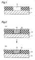
- Fig. 1 is a schematic sectional view of a substrate provided with wiring channels for use in the process for producing an integrated circuit according to the present invention.
- numeral 1 denotes a substrate
- numeral 2 an insulating film
- numeral 3 a wiring channel.
- the substrate 1 for use in the present invention can be constituted of silicon, glass or the like.
- the insulating film 2 is formed on the above substrate.
- the insulating film is not particularly limited as long as it is constituted of an insulating material.
- it is constituted of silica, alumina, titania, silicon nitride, silicon carbide, an organic resin polymer, plasma TEOS (plasma TEOS refers to a product of plasma vapor deposition of tetraethyl orthosilicate (TEOS)) or the like.
- the insulating film 2 may be constituted of a single material or a mixture of a plurality of materials. Further, the insulating film 2 may have a multilayer structure consisting of varied insulating films arranged vertically.
- the insulating film 2 can be formed by known methods. For example, it can be formed by the spin coating method, CVD method, sputtering method, plasma CVD method, or the like.
- an insulating film of silica (SOG film) disclosed in Japanese Patent Laid-open Publication No. 2(1990)-237030 relating to another application of the applicant is preferred from the viewpoint of high contact resistance, low dielectric constant and excellent planarity.
- the thickness of the above insulating film is preferably in the range of 0.1 to 6 ⁇ m.
- the thickness of the insulating film 2 When the thickness of the insulating film 2 is less than 0.1 ⁇ m, the thickness may be too small to ensure the insulation. On the other hand, when the thickness of the insulating film 2 exceeds 6 ⁇ m, the insulating film 2 may suffer cracking.
- the substrate with wiring channels for use in the present invention it is not necessarily needed to provide a monolayer insulating film as shown in Fig. 1 , and a laminate of a plurality of insulating films as mentioned above may be provided.
- the laminate of a plurality of insulating films it is preferred that the final thickness of insulating film laminate be in the range of 0.1 to 6 ⁇ m.
- the insulating film is provided with wiring channels.
- the depth (Dc) of wiring channels is preferably in the range of 0.05 to 10 ⁇ m, still preferably 0.1 to 5 ⁇ m.
- the width (Wc) of wiring channels is preferably in the range of 0.05 to 100 ⁇ m, still preferably 0.1 to 20 ⁇ m.
- the width (Wc) of wiring channels is less than 0.05 ⁇ m, the width may be too small to selectively feed conductive fine particles into the wiring channels.
- the width (Wc) of wiring channels exceeds 100 ⁇ m, the width of wiring channels may be too large to form a circuit of high density.
- conductive fine particles formed as a result of exposure of the component for conductive fine particle formation to ultrasonic waves, or conductive fine particles contained in advance absorb energy of exposure ultrasonic waves.
- dense deposition of conductive fine particles can be accomplished while the conductive fine particles collide against the bottom and side wall of wiring channels or collide against sequentially deposited conductive fine particles. Consequently, junction surfaces of conductive fine particles can be increased to thereby enable forming a circuit of low circuitry resistance.
- a circuit exhibiting high adherence to the bottom or side wall of wiring channels (occasionally, barrier metal formed in wiring channels as mentioned later) can be formed.
- the width of circuit must be increased for ensuring the conductivity of circuit, so that forming of a circuit of high density may be disenabled.
- the thickness of wiring layers may be too large to obtain an integrated circuit exhibiting high integration in the direction of height.
- the ratio (Dc/Wc) between the depth (Dc) of wiring channels and the width (Wc) of wiring channels is preferably in the range of 0.1 to 20. Even if the depth (Dc) of wiring channels and the width (Wc) of wiring channels fall within the above ranges, when the ratio Dc/Wc, referred to as "aspect ratio", is less than 0.1, the conductivity of circuit may not be ensured. Increasing the width of circuit for coping with this problem may disenable forming a circuit of high density. On the other hand, when the aspect ratio Dc/Wc exceeds 20, the conductivity of circuit may not be ensured. Increasing the height of circuit for coping with this problem may disenable forming a circuit exhibiting high integration in vertical direction.
- These wiring channels can be formed by providing a 0.1 to 10 ⁇ m line-and-space photoresist film (PR film) on a substrate and subsequently performing sputtering thereon.
- PR film line-and-space photoresist film
- a barrier metal layer may be formed on the inner surface of wiring channels before the application of the coating liquid for integrated circuit formation.
- known methods can be employed.
- the barrier metal layer can be formed by sputtering of TiN, Ta, TaN or the like.
- the thickness of the barrier metal layer is generally in the range of 50 to 200 nm.
- the formation of the barrier metal layer enables not only preventing the diffusion of conductive fine particle components for circuit formation, organic stabilizers described later and impurities such as ions into the insulating film or the corrosion of the insulating film therewith but also inhibiting the drop of insulating capability of insulating film attributed to the above diffusion into and corrosion of the insulating film.
- the formation of circuit is carried out by coating the substrate provided with wiring channels with the coating liquid for integrated circuit formation while being exposed to ultrasonic waves, optionally followed by drying and thermal treatment.
- the coating liquid for integrated circuit formation for use in the present invention comprises a component for conductive fine particle formation and/or conductive fine particles and a solvent.
- the component for conductive fine particle formation maybe contained alone, or conductive fine particles may be contained alone.
- the component for conductive fine particle formation may be contained together with conductive fine particles.
- the solvent may be water, or an organic solvent, or a mixture of water and an organic solvent.
- the component for conductive fine particle formation refers to a component capable of forming conductive fine particles, such as the following metal fine particles of single component or composite metal fine particles containing a plurality of metal components, and there can be mentioned metal ions.
- metal ions include ions of metals such as Au, Ag, Pd, Pt, Rh, Ru, Cu, Fe, Ni, Co, Sn, Ti, In, Al, Ta, Sb and W. Of these, ions of metals including Au, Ag, Pd, Pt, Rh and Cu are preferred.
- This component for conductive fine particle formation when exposed to ultrasonic waves, easily forms metal colloid fine particles of diameter approximately equal to that of the following conductive fine particles.
- Any conductive fine particles can be used without particular limitation as long as conductivity is exhibited.
- use can be made of metal fine particles, metal oxide fine particles, conductive carbon and conductive polymer fine particles.
- metal fine particles are preferably used as the conductive fine particles.
- metal fine particles can be used as the metal fine particles, which may be metal fine particles of single component or composite metal fine particles containing a plurality of metal components.
- the plurality of metals constituting the composite metal fine particles may form an alloy being in the state of a solid solution, a eutectic not being in the state of a solid solution or a mixture of such an alloy and such a eutectic.
- the metal oxidation and ionization are inhibited, so that, for example, the particulate growth of composite metal fine particles is inhibited.
- the reliability of the composite metal fine particles is high in that, for example, their corrosion resistance is high and the deterioration of their conductivity (rise of resistance value) is slight.
- Metal fine particles comprising at least one metal selected from the group consisting of Au, Ag, Pd, Pt, Rh, Ru, Cu, Fe, Ni, Co, Sn, Ti, In, Al, Ta, Sb and W are preferably used as the above metal fine particles.
- the metal fine particles there can be mentioned fine particles of a metal selected from the group consisting of Au, Ag, Pd, Pt, Rh, Ru, Cu, Fe, Ni, Co, Sn, Ti, In, Al, Ta, Sb and W.
- composite metal fine particles there can be mentioned those composed of at least two of metals selected from the group consisting of Au, Ag, Pd, Pt, Rh, Ru, Cu, Fe, Ni, Co, Sn, Ti, In, Al, Ta, Sb and W.
- Preferred combinations of two or more types of metals include, for example, Au-Cu, Ag-Pt, Ag-Pd, Au-Pd, Au-Rh, Pt-Pd, Pt-Rh, Fe-Ni, Ni-Pd, Fe-Co, Cu-Co, Ru-Ag, Au-Cu-Ag, Ag-Cu-Pt, Ag-Cu-Pd, Ag-Au-Pd, Au-Rh-Pd, Ag-Pt-Pd, Ag-Pt-Rh, Fe-Ni-Pd, Fe-Co-Pd and Cu-Co-Pd.
- metal fine particles of a metal such as Au, Ag, Pd, Pt, Rh, Cu, Co, Sn, In or Ta
- part thereof may be in oxidized form.
- the metal fine particles may contain an oxide of the metal.
- compounds having bonded P or B atoms may be contained in the metal fine particles.
- the metal fine particles can be obtained by known processes (see Japanese Patent Laid-open Publication No. 10(1998)-188681 ).
- the metal fine particles can be prepared by a process wherein, in a mixed solvent of an alcohol and water, a single metal salt is reduced, or a plurality of metal salts are simultaneously or separately reduced.
- a reducing agent may be added according to necessity.
- suitable reducing agents include ferrous sulfate, trisodium citrate, tartaric acid, sodium borohydride and sodium hypophosphite.
- heat treatment maybe performed in a pressure vessel at about 100°C or higher.
- the metal fine particles can be prepared by another process, which comprises providing a dispersion of fine particles of a single-component metal or fine particles of an alloy and causing fine particles or ions of a metal having a normal hydrogen electrode potential higher than that of the above single-component metal fine particles or alloy fine particles to be present in the dispersion to thereby precipitate the metal of higher normal hydrogen electrode potential on the single-component metal fine particles and/or alloy fine particles.
- a metal of still higher normal hydrogen electrode potential may be further precipitated on the thus obtained composite metal fine particles.
- the metal exhibiting the highest normal hydrogen electrode potential be abundant in the surface layer of the composite metal fine particles.
- the presence in abundance of the metal exhibiting the highest normal hydrogen electrode potential in the surface layer of the composite metal fine particles would inhibit the oxidation and ionization of the composite metal fine particles to thereby enable suppressing the particulate growth attributed to, for example, ion migration.
- these composite metal fine particles have high corrosion resistance, so that the deterioration of conductivity can be suppressed.
- the metal fine particles can be prepared by the ultrasonic wave exposure direct reduction method described on, for example, page 70 of Abstracts of Papers (1997 ) presented before Symposium of General Autumn Meeting held by the Metallurgical Society of Japan.
- the metal fine particles can be prepared by exposing a solution containing noble metal ions (for example, Ag + , Au 3+ , Pd 2+ , Pt 2+ or Pt 4+ ) and having an organic compound such as a surfactant added thereto according to necessity to ultrasonic waves in an inert gas atmosphere at, for example, 200 kHz and 6 W/cm 2 .
- noble metal ions for example, Ag + , Au 3+ , Pd 2+ , Pt 2+ or Pt 4+
- organic compound such as a surfactant added thereto according to necessity to ultrasonic waves in an inert gas atmosphere at, for example, 200 kHz and 6 W/cm 2 .
- the average diameter of these metal fine particles preferably ranges from 1 to 200 nm, still preferably from 2 to 70 nm.
- the metal fine particles When the average diameter of the metal fine particles exceeds 200 nm, the metal fine particles are too large to enter the wiring channels. Even if the metal fine particles manage to enter the wiring channels, dense deposition thereof cannot be effected to thereby render forming of a circuit of low resistance value difficult.
- the surface resistance between deposited particles may be increased so sharply that a circuit exhibiting a resistance value as low as capable of attaining the object of the present invention cannot be formed.
- conductive metal oxide fine particles may be used in place of the above metal fine particles, or in combination with the above metal fine particles.
- the conductive metal oxide there can be mentioned, for example, tin oxide, tin oxide doped with Sb, F or P, indium oxide, indium oxide doped with Sn or F, antimony oxide or low-order titanium oxide.
- the average diameter of these conductive metal oxide fine particles be 70% or less of the width of wiring channels and range from 1 to 200 nm, especially from 2 to 70 nm.
- the coating liquid for integrated circuit formation for use in the present invention may contain conductive fine particles other than the above metal fine particles and the above metal oxide fine particles.
- inorganic conductive fine particles such as conductive carbon
- conductive fine particles constituted of a conductive polymer such as polyacetylene, polypyrrole or poly-p-phenylene.
- the average diameter of these conductive fine particles range from 1 to 200 nm, especially from 2 to 70 nm.
- organic solvent for use in the coating liquid for integrated circuit formation there can be mentioned, for example, alcohols such as methanol, ethanol, propanol, butanol, diacetone alcohol, furfuryl alcohol, tetrahydrofurfuryl alcohol, ethylene glycol and hexylene glycol; esters such as methyl acetate and ethyl acetate; ethers such as diethyl ether, ethylene glycol monomethyl ether, ethylene glycol monoethyl ether, ethylene glycol monobutyl ether, diethylene glycol monomethyl ether and diethylene glycol monoethyl ether; and ketones such as acetone, methyl ethyl ketone, acetylacetone and acetoacetic esters. These may be used individually or in combination.
- alcohols such as methanol, ethanol, propanol, butanol, diacetone alcohol, furfuryl alcohol, tetrahydrofurfuryl alcohol, ethylene glyco
- the concentration of component for conductive fine particle formation and/or conductive fine particles in the coating liquid for integrated circuit formation is not particularly limited as long as the fluidity of coating liquid can be ensured, it is preferred that the component for conductive fine particle formation and/or conductive fine particles be contained in an amount, in terms of solid contents or metal (in terms of formed metal or composite metal fine particles with respect to the component for conductive fine particle formation and in terms of the total thereof when the component for conductive fine particle formation and conductive fine particles are contained; the same applies hereinafter), of 0.05 to 30% by weight, especially 0.1 to 10% by weight, and still especially 0.2 to 5% by weight.
- the concentration is so low that repeated applications are inevitably needed. Further, the evaporation of solvent takes time, so that a prolonged period of time is required for circuit formation.
- the coating liquid for integrated circuit formation for use in the present invention may contain a component for matrix formation which acts as a binder of conductive fine particles after the formation of an integrated circuit or acts as a binder between the same and wiring channel walls (including barrier metal walls).
- This component for matrix formation is preferably constituted of a precursor of at least one oxide selected from among silica, silica-based composite oxides, zirconia and antimony oxide in the present invention.
- a product obtained by hydrolysis and polycondensation of an organosilicon compound such as an alkoxysilane, or silicic acid obtained by dealkalizing an aqueous solution of alkali metal silicate is preferably used.
- resins for use in paints can be employed as the component for matrix formation.
- This component for matrix formation is appropriately contained in an amount, in terms of oxide (in the use of an inorganic compound) or resin, of 0.01 to 0.5 part by weight, preferably 0.03 to 0.2 part by weight, per part by weight of metal with respect to the amount, in terms of solid contents or metal, of component for conductive fine particle formation and/or conductive fine particles.
- an organic stabilizer or a surfactant may be contained in the coating liquid for integrated circuit formation in order to accelerate the formation of metal fine particles, or to improve the dispersion performance of metal fine particles, or to enhance the stability of dispersion.
- organic stabilizer or surfactant there can be mentioned, for example, gelatin, polyvinyl alcohol and polyvinylpyrrolidone; oxalic acid, malonic acid, succinic acid, glutaric acid, adipic acid, sebacic acid, maleic acid, fumaric acid, phthalic acid, citric acid and other polybasic carboxylic acids and salts thereof; and further sulfonic acid salts, organosulfonic acid salts, phosphoric acid salts, organophosphoric acid salts, heterocyclic compounds, polycarboxylic acids and mixtures of these compounds.
- the amount of organic stabilizer or surfactant is varied depending on the type thereof, the diameter of metal fine particles, etc., the organic stabilizer or surfactant can appropriately be contained in the coating liquid in an amount of 0.005 to 5 parts by weight, preferably 0.01 to 2 parts by weight, per part by weight of metal with respect to the amount, in terms of solid contents or metal, of component for conductive fine particle formation and/or conductive fine particles (metal fine particles) .
- the amount of organic stabilizer or surfactant is less than 0.005 part by weight, desirable dispersion and stability performance cannot be realized.
- the amount of organic stabilizer or surfactant is larger than 5 parts by weight, a conductivity deterioration may be caused.
- the conductive fine particles in particular, metal fine particles are used in the state of being dispersed in water and/or an organic solvent
- the total concentration of ions including alkali metal ions, ammonium ion, polyvalent metal ions, inorganic anions such as mineral acid anions, and organic anions such as acetic acid and formic acid anions, which are liberated from the particles and present in the coating liquid be 10 mmol or less per 100 g of solid contents contained in the dispersion.
- inorganic anions such as mineral acid anions are detrimental to the stability and dispersibility of metal fine particles, so that the smaller the amount thereof in the dispersion, the greater the preference.
- the dispersion condition of metal fine particles contained in the coating liquid for integrated circuit formation is excellent.
- a coating liquid in which substantially no aggregated particles are contained can be obtained.
- the monodisperse condition of metal fine particles in the coating liquid can be maintained during the course of circuit formation. Accordingly, when an integrated circuit is formed from the coating liquid for integrated circuit formation having a low ion concentration, a dense circuit of low resistance value can be obtained because of the absence of aggregated particles.
- conductive fine particles such as metal fine particles can be appropriately dispersed and aligned. Consequently, there can be provided an integrated circuit of high reliability with no defect as compared with circuits wherein conductive fine particles are aggregated.
- the method of deionizing for obtaining the above coating liquid of low ion concentration is not particularly limited if finally the ion concentration of the coating liquid falls within the above range.
- preferred deionization methods there can be mentioned one in which either the dispersion of conductive fine particles as a feedstock for the coating liquid or the coating liquid for integrated circuit formation prepared from the dispersion is brought into contact with a cation exchange resin and/or an anion exchange resin, and another method in which these liquids are purified with an ultrafilter membrane.
- the method of applying the coating liquid for integrated circuit formation is not particularly limited as long as the wiring channels can be coated with the coating liquid for integrated circuit formation while being exposed to ultrasonic waves, it is preferred that the application be effected in such a manner that the coating liquid flowing out of, for example, a nozzle fitted to a vessel can uniformly be exposed to ultrasonic waves and that selective application to the wiring channels can be accomplished.
- the coating liquid for integrated circuit formation during application is exposed to ultrasonic waves.
- the coating liquid while dropping from or flowing out of the above nozzle or the like and/or the coating liquid having been deposited in the wiring channels is exposed to ultrasonic waves.
- the ultrasonic wave exposure conditions are varied depending on the concentration, in terms of metal, of component for metal fine particle formation in the coating liquid for integrated circuit formation, the concentration and average diameter of conductive fine particles in the coating liquid for integrated circuit formation, the boiling point of solvent, the application speed of coating liquid, etc. and are not particularly limited as long as conductive fine particles can selectively be applied into the wiring channels, appropriate selection can be made within the range of 20 to 400 kHz and within the range of 5 to 400 W.
- the coating liquid for integrated circuit formation contains the component for conductive fine particle formation
- the exposure to ultrasonic waves brings about not only heating of the coating liquid but also formation of conductive fine particles.
- the coating liquid is concentrated, dried and enter the wiring channels with the result that conductive fine particles are deposited in the wiring channels to thereby form a layer of conductive fine particles in the wiring channels.
- a circuit is formed.
- the coating liquid for integrated circuit formation contains conductive fine particles
- the exposure to ultrasonic waves brings about heating of the coating liquid.
- the coating liquid is concentrated, dried and enter the wiring channels with the result that conductive fine particles are deposited in the wiring channels to thereby form a layer of conductive fine particles in the wiring channels.
- a circuit is formed.
- the thus formed conductive fine particles including metal fine particles absorb the energy of ultrasonic waves. Consequently, the conductive fine particles having entered the wiring channels would collide against the bottom and side wall of wiring channels and collide with each other, so that conductive fine particles would be densely deposited sequentially from the bottom of wiring channels to thereby form a circuit.
- second ultrasonic wave exposure After the formation of a circuit by satisfactorily filling the wiring channels, a further exposure to ultrasonic waves (second ultrasonic wave exposure) may be effected according to necessity.
- the coating liquid for integrated circuit formation can be applied by the spinner method before carrying out the second ultrasonic wave exposure.
- This second ultrasonic wave exposure enables planarizing the upper surface of substrate after the circuit formation, thereby facilitating the planarizing operation (for example, chemical machine polishing (CMP)) performed after the circuit formation according to necessity.
- CMP chemical machine polishing
- the method of forming an integrated circuit according to the present invention enables selective dense deposition of conductive fine particles in the wiring channels and filling the wiring channels with conductive fine particles to thereby form a circuit in such a fashion that the upper end surface of wiring channels is substantially in agreement with the upper end surface of conductive fine particle layer. Therefore, the formation of conductive layer (sacrificial layer) high over the upper end surface of wiring channels as observed in the conventional plating method, CVD method and PVD method and in the above-mentioned SOM method can be restricted, so that the planarizing operation can be strikingly facilitated and that the end surface after the planarizing operation is excellent in planarity. Accordingly, an economic advantage can be ensured in the formation of integrated circuit.
- the application of the coating liquid for integrated circuit formation under exposure to ultrasonic waves is optionally followed by heating (curing) at about 200 to 400°C in an oxidative and/or reducing atmosphere or in an inert gas atmosphere.
- This heating not only removes impurities if any in the circuit but also promotes the junction of conductive fine particles, so that a circuit of low resistance value exhibiting excellent adherence to the wiring channels can be obtained.
- the wiring channels are fitted with the barrier metal layer, a circuit of especially high adherence can be obtained.
- the formed conductive fine particle layer is preferably subjected to planarizing operation.
- Fig. 2 is a schematic view showing an outline of planarizing operation.
- Numeral 11 denotes a substrate, numeral 12 an insulating film, numeral 13 a formed conductive fine particle layer, and numeral 14 a barrier metal layer.
- the conductive fine particle layer immediately after the formation thereof is disposed on not only the wiring channels but also the surface of insulating film.
- the conductive fine particle layer is planarized so that, referring to Fig. 2(2) , horizontally and in planar form, the upper end surface of conductive fine particle layer after polishing planarization is agreement with the upper end surface of insulating film.
- This planarizing operation is performed by, for example, chemical machine polishing (CMP).
- CMP chemical machine polishing
- the thus removed portion of conductive fine particle layer may be called a sacrificial layer.
- an insulating film (second insulating film) may be provided on the circuit surface.
- the method of forming the second insulating film is the same as for the above insulating film.
- connecting channels for electrical connection with the formed circuit are provided at given positions of the second insulating film.
- the connecting channels can be formed by, for example, dry etching and generally have a diameter of about 1.5 ⁇ m.
- a substrate with multilayer integrated circuit can be produced by repeating the above sequence of operations including formation of the insulating film, formation of wiring channels, application of the coating liquid for integrated circuit formation to wiring channels and connecting channels and formation of the second insulating film.
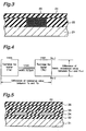
- Fig. 3 is a schematic sectional view of one form of substrate with integrated circuit according to the present invention.
- numeral 21 denotes a substrate
- numeral 22 the first insulating film
- numeral 23 a wiring layer
- numeral 24 the second insulating film.
- the substrate 21 is laminated with the first insulating film 22.
- the wiring layer 23 is provided in the insulating film by the method described above.
- the second insulating film 24 is superimposed on the insulating film 22 and circuit. (These are referred to as "the first wiring layer").
- the second wiring layer (not shown) of the same constitution as that of the first wiring layer is formed on the second insulating film 24.
- the first wiring layer and the second wiring layer are connected to each other by means of through-holes (connecting channels, not shown).
- the third wiring layer, Vietnamese , n-th wiring layer are formed.
- vertically arranged wiring layers are connected to each other by means of through-holes (connecting channels, not shown).
- connection of wiring layers can be accomplished by providing each insulating film with through-holes (connecting channels) of given diameter (generally about 1.5 ⁇ m) by dry etching, for example, RIE (Reactive Ion Etching) and thereafter effecting sputtering.
- the connection can be accomplished by, at the time of forming an upper-layer circuit, applying the coating liquid for integrated circuit formation under exposure to ultrasonic waves in the same manner as in the above circuit formation so as to densely deposit conductive fine particles in the wiring channels and connecting channels.
- the coating liquid for integrated circuit formation while being exposed to ultrasonic waves to the wiring channels Upon the application of the coating liquid for integrated circuit formation while being exposed to ultrasonic waves to the wiring channels according to the present invention, when the coating liquid contains the component for conductive fine particle formation, the exposure to ultrasonic waves leads to formation of conductive fine particles and causes the temperature of coating liquid to rise, thereby evaporating the dispersion medium of coating liquid, so that coating while the coating liquid is being concentrated can be performed. Furthermore, the vibrational energy of ultrasonic waves is transmitted to conductive fine particles, so that the conductive fine particles would collide against the wall of wiring channels, thereby particles would be aligned densely by impact at colliding. Therefore, even when the width of wiring channels is limited, conductive fine particles can be selectively and densely formed into a laminate in the wiring channels.
- the coating liquid contains conductive fine particles
- the exposure to ultrasonic waves causes the temperature of coating liquid to rise, thereby evaporating the dispersion medium of coating liquid, so that coating while the coating liquid is being concentrated can be performed.
- the vibrational energy of ultrasonic waves is transmitted to conductive fine particles, so that the conductive fine particles would collide against the wall of wiring channels to thereby cause impacts, which impacts would realize dense alignment of particles. Therefore, even when the width of wiring channels is limited, conductive fine particles can be selectively and densely formed into a laminate in the wiring channels.
- the process for producing an integrated circuit according to the present invention enables densely depositing conductive fine particles in wiring channels even when the width of wiring channels is limited. Consequently, a circuit of low resistance value and high density can be formed. Therefore, even when the chip size is large, an increase of propagation delay time of electrical signal can be avoided.
- the process of the present invention enables forming a circuit in such a fashion that the upper end surface of wiring channels is substantially in agreement with the upper end surface of conductive fine particle layer. Therefore, the formation of conductive layer high over the upper end surface of wiring channels can be restricted, so that the planarizing operation can be strikingly facilitated and that the end surface after the planarizing operation is excellent in planarity. Accordingly, the process of the present invention ensures an economic advantage in the production of substrate with integrated circuit.
- a circuit of high-degree integration in not only the longitudinal direction but also the lateral direction is formed in the obtained substrate with integrated circuit. This leads to a reduction of propagation delay time and to an increase of reliability.
- compositions of dispersions of metal fine particles and conductive fine particles used in the Examples and Comparative Examples are specified in Table 1.
- Dispersions of metal fine particles (Q-1, Q-2 and Q-3) were prepared in the following manner.
- trisodium citrate was added to 100 g of pure water in an amount corresponding to 0.01 part by weight per part by weight of metal fine particles.
- Aqueous solutions of silver nitrate, palladium nitrate and copper chloride were added thereto so that the concentration in terms of metal was 10% by weight and so that the metal species had weight ratios specified in Table 1.
- an aqueous solution of ferrous sulfate was added in a molar amount equal to the total mole of silver nitrate, palladium nitrate and copper chloride and agitated for 1 hr in an atmosphere of nitrogen.
- dispersions of metal fine particles were obtained.
- a solvent of a 3 : 1 by weight mixture of ethanol and 1-ethoxy-2-propanol was added to each of the above prepared metal fine particle dispersions (S-1, S-2 and S-3) to thereby accomplish dilution.
- coating liquids for integrated circuit formation of 0.5% by weight concentration SC-1, SC-2 and SC-3) were obtained.
- the coating liquids SC-1, SC-2 and SC-3 correspond to metal fine particle dispersions S-1, S-2 and S-3, respectively.
- trisodium citrate was added to 100 g of pure water in an amount corresponding to 0.01 part by weight per part by weight, in terms of metal, of component for metal fine particle formation.
- Silvernitrate, palladiumnitrate and copper chloride were dissolved therein so that the concentration in terms of metal was 0.5% by weight and so that the metal species had weight ratios specified in Table 2.
- sodium dodecylsulfate as a surfactant was added to each of the solutions in an amount corresponding to 1 part by weight per part by weight, in terms of metal, of component for metal fine particle formation, and agitated for 30 min in an atmosphere of nitrogen.
- coating liquids for integrated circuit formation containing component for metal fine particle formation (SB-1, SB-2 and SB-3) were obtained.
- Table 2 Coating liq. Component Wt. ratio Concn. in terms of metal SB-1 Ag/Pd 8/2 0.5 SB-2 Ag/Pd 6/4 0.5 SB-3 Cu - 0.5
- Coating liquid for integrated circuit formation containing not only component for metal fine particle formation but also metal fine particles (SD-1) was prepared by mixing the above coating liquid for integrated circuit formation (SB-1) with the above coating liquid for integrated circuit formation (SC-1) at a weight ratio of 1 : 1.
- the above prepared dispersion for integrated circuit formation (SC-1) was placed in a container equipped with a nozzle of 5 mm diameter.
- the substrate provided with wiring channels was coated with the dispersion for integrated circuit formation (SC-1) fed through the nozzle.
- the dispersion for integrated circuit formation (SC-1) was applied along the above formed wiring channels while exposing the same to ultrasonic waves of 27 kHz and 300 W generated by ultrasonic wave emitter (AUTOCHDER-300, model 5271, manufactured by Kaijo Denki K.K.), thereby depositing metal fine particles (Q-1) in the wiring channels.
- AUTOCHDER-300, model 5271, manufactured by Kaijo Denki K.K. ultrasonic wave emitter
- metal fine particle layers piled slightly high over the upper end surface of wiring channels were subjected to CMP planarizing and cured in a nitrogen atmosphere at 400°C for 30 min. Further, a 200 nm thick SiO 2 film (insulating film) was formed thereon by the CVD technique. Thus, an intended substrate with integrated circuit (A) was obtained.
- the circuit conductivity and denseness of deposited particles were inspected.
- the sacrificial layer (see Fig. 2 ) on the substrate after coating and drying was polished by means of polishing apparatus (Wafer Polishing System NF-300, manufactured by Nanofactor K.K.) under a load of 200 g/cm 2 at a wafer to polishing pad relative speed of 450 cm/min.
- polishing apparatus Wafer Polishing System NF-300, manufactured by Nanofactor K.K.
- the relative difficulty of polishing was evaluated on the following criterion based on time required for polishing:
- the silicon wafer substrate was coated with a positive photoresist, and subjected to an exposure of resist portions for one 0.3 ⁇ m line and tester terminals (Ta and Tb) as shown in Fig. 4 . Subsequently, the exposed portions were removed, and underlayer insulating films were patterned with the use of a mixture of CF 4 and CHF 3 gases. The remaining resist was removed by irradiating the same with O 2 plasma. Thus, wiring channels having a width (Wc) of 0.3 ⁇ m, a depth (Dc) of 0.6 ⁇ m and an aspect ratio (Dc/Wc) of 2 were formed. A tester was connected to the tester terminals, and the value of resistance (between Ta and Tb) was measured.
- Wc width
- Dc depth
- Dc/Wc aspect ratio
- circuit density was evaluated by observation of SEMs at the time of evaluating the planarity after the coating with the coating liquid for integrated circuit formation:
- Substrate with integrated circuit (B) was produced in the same manner as in Example 1 except that wiring channels having a width (Wc) of 0.4 ⁇ m, a depth (Dc) of 1.6 ⁇ m and an aspect ratio (Dc/Wc) of 4 were formed and that the coating liquid for integrated circuit formation (SC-2) was used.
- Substrate with integrated circuit was produced in the same manner as in Example 1 except that the dispersion for integrated circuit formation (SC-3) was used.
- Example 1 The same procedure as in Example 1 was repeated except that, without the exposure to ultrasonic waves, the dispersion for integrated circuit formation (SC-1) was applied by the spinner method and dried at 90°C for 5 min.
- Substrate with conductor integrated circuit (D) was produced in the same manner as in Example 1 except that the above application and drying was repeated 20 times, thereby depositing metal fine particles (Q-1) in wiring channels so as to form a circuit. After the application performed 20 times, metal fine particles were so thickly deposited on the insulating film that portions on the insulating film were protrudent while portions on the wiring channels were depressed, thereby forming an uneven surface.
- Substrate with integrated circuit (E) was produced in the same manner as in Example 1 except that wiring channels having a width (Wc) of 0.2 ⁇ m, a depth (Dc) of 0.8 ⁇ m and an aspect ratio (Dc/Wc) of 4 were formed, except that, without the exposure to ultrasonic waves, the dispersion for integrated circuit formation (SC-1) was applied by the spinner method and dried at 90°C for 5 min, and except that the application and drying was repeated 20 times, thereby depositing metal fine particles (Q-1) in the wiring channels so as to form a circuit. After the application performed 20 times, deposition of conductive fine particles was observed on the insulating film and the wiring channels, which conductive fine particles exhibited the same substantial planarity as in Example 1.
- Substrate with integrated circuit (F) was produced in the same manner as in Example 1 except that the dispersion for integrated circuit formation (SB-1) was used.
- Substrate with integrated circuit (G) was produced in the same manner as in Example 1 except that the dispersion for integrated circuit formation (SB-2) was used.
- Substrate with integrated circuit (H) was produced in the same manner as in Example 1 except that the dispersion for integrated circuit formation (SB-3) was used.
- Substrate with integrated circuit (I) was produced in the same manner as in Example 1 except that the dispersion for integrated circuit formation (SD-1) was used.
- the integrated circuits formed under exposure to ultrasonic waves realize efficient dense deposition of conductive fine particles in minute wiring channels and connecting holes, so that they provide a circuit of high conductivity (low wiring resistance) and high density. Further, therefor, the planarizing can be accomplished easily.
- the polishing for enhanced planarity is difficult, and the circuit conductivity is not satisfactory. Further, these integrated circuits cannot provide a circuit of high density.
Landscapes
- Engineering & Computer Science (AREA)
- Physics & Mathematics (AREA)
- Condensed Matter Physics & Semiconductors (AREA)
- General Physics & Mathematics (AREA)
- Manufacturing & Machinery (AREA)
- Computer Hardware Design (AREA)
- Microelectronics & Electronic Packaging (AREA)
- Power Engineering (AREA)
- Internal Circuitry In Semiconductor Integrated Circuit Devices (AREA)
Abstract
Claims (7)
- Procédé pour produire un circuit intégré, comprenant le revêtement d'un substrat pourvu de canaux de câblage d'une largeur donnée et d'une profondeur donnée en utilisant un liquide de revêtement pour la formation d'un circuit intégré qui contient un solvant et entre 0,05 % en poids et 30 % en poids d'au moins soit un composant pour former de fines particules conductrices lors de l'application d'ultrasons, soit de fines particules conductrices, afin de former ainsi un circuit intégré sur le substrat, et dans lequel les fines particules conductrices présentent un diamètre de particule moyen qui correspond à 70 %, ou moins, de la largeur des canaux de câblage et qui est comprise dans la gamme de 1 nm à 200 nm, et l'exposition du liquide de revêtement pour la formation d'un circuit intégré à des ondes ultrasoniques lorsque le liquide de revêtement est appliqué aux canaux de câblage,
dans lequel les ondes ultrasoniques chauffent le liquide de revêtement dans le but de faire s'évaporer le solvant, forment de fines particules conductrices à partir du composant prévu pour former de fines particules conductrices si un tel composant est présent, et concentrent le liquide de revêtement. - Procédé selon la revendication 1, comprenant en outre la planarisation d'une surface de revêtement qui résulte du revêtement réalisé avec le liquide de revêtement pour la formation d'un circuit intégré.
- Procédé selon la revendication 1 ou 2, dans lequel les fines particules conductrices sont de fines particules de métal qui comprennent au moins un métal qui est sélectionné dans le groupe comprenant l'Au, l'Ag, le Pd, le Pt, le Rh, le Ru, le Cu, le Fe, le Ni, le Co, le Sn, le Ti, l'In, l'Al, le Ta, le Sb et le W.
- Procédé selon l'une quelconque des revendications 1 à 3, dans lequel la profondeur (D) des canaux de câblage est comprise dans la gamme de 0,05 µm à 10 µm, la largeur (Wc) des canaux de câblage est comprise dans la gamme de 0,05 µm à 100 µm, et le rapport entre la profondeur (D) des canaux de câblage et la largeur (Wc) des canaux de câblage (D/Wc) est comprise dans la gamme de 0,1 à 20.
- Procédé selon l'une quelconque des revendications précédentes, dans lequel le liquide de revêtement pour la formation d'un circuit intégré contient un solvant organique.
- Procédé selon l'une quelconque des revendications précédentes, dans lequel le liquide de revêtement pour la formation d'un circuit intégré contient un stabilisant organique.
- Procédé selon l'une quelconque des revendications précédentes, dans lequel la concentration totale en ions dans le liquide de revêtement est de 10 millimoles ou moins par 100 g de contenu solide contenu dans la dispersion.
Applications Claiming Priority (3)
| Application Number | Priority Date | Filing Date | Title |
|---|---|---|---|
| JP2000133674 | 2000-05-02 | ||
| JP2000133674 | 2000-05-02 | ||
| PCT/JP2001/003451 WO2001084610A1 (fr) | 2000-05-02 | 2001-04-23 | Procede de realisation d'un circuit integre, et substrat dote d'un circuit integre forme a l'aide dudit procede |
Publications (3)
| Publication Number | Publication Date |
|---|---|
| EP1280193A1 EP1280193A1 (fr) | 2003-01-29 |
| EP1280193A4 EP1280193A4 (fr) | 2006-01-04 |
| EP1280193B1 true EP1280193B1 (fr) | 2011-06-29 |
Family
ID=18642112
Family Applications (1)
| Application Number | Title | Priority Date | Filing Date |
|---|---|---|---|
| EP01921998A Expired - Lifetime EP1280193B1 (fr) | 2000-05-02 | 2001-04-23 | Procede de realisation d'un circuit integre, et substrat dote d'un circuit integre forme a l'aide dudit procede |
Country Status (6)
| Country | Link |
|---|---|
| US (1) | US7163892B2 (fr) |
| EP (1) | EP1280193B1 (fr) |
| JP (1) | JP4578755B2 (fr) |
| KR (1) | KR100805128B1 (fr) |
| TW (1) | TW544788B (fr) |
| WO (1) | WO2001084610A1 (fr) |
Families Citing this family (15)
| Publication number | Priority date | Publication date | Assignee | Title |
|---|---|---|---|---|
| JP2002141351A (ja) * | 2000-10-31 | 2002-05-17 | Japan Science & Technology Corp | 回路基板とその金属配線形成方法 |
| JP3951750B2 (ja) * | 2002-03-07 | 2007-08-01 | セイコーエプソン株式会社 | 物質充填方法、膜形成方法、デバイスおよびデバイスの製造方法 |
| CN1301048C (zh) * | 2003-03-03 | 2007-02-14 | 精工爱普生株式会社 | 配线基板的制造方法 |
| US7384862B2 (en) * | 2003-06-30 | 2008-06-10 | Semiconductor Energy Laboratory Co., Ltd. | Method for fabricating semiconductor device and display device |
| JP2005142473A (ja) * | 2003-11-10 | 2005-06-02 | Semiconductor Leading Edge Technologies Inc | 半導体装置の製造方法 |
| JP2006173408A (ja) * | 2004-12-16 | 2006-06-29 | Catalysts & Chem Ind Co Ltd | 回路付基板の製造方法および該方法で得られた回路付基板 |
| US7611969B2 (en) * | 2005-02-17 | 2009-11-03 | University Of Houston | Generation and applications of negative dielectric constant materials |
| TWI297513B (en) * | 2005-10-06 | 2008-06-01 | Ind Tech Res Inst | Electrode and method for forming the same |
| US9439293B2 (en) | 2007-11-21 | 2016-09-06 | Xerox Corporation | Galvanic process for making printed conductive metal markings for chipless RFID applications |
| JP6202798B2 (ja) * | 2011-10-12 | 2017-09-27 | エーエスエム インターナショナル エヌ.ヴェー.Asm International N.V. | 酸化アンチモン膜の原子層堆積 |
| JP6360276B2 (ja) * | 2012-03-08 | 2018-07-18 | 東京エレクトロン株式会社 | 半導体装置、半導体装置の製造方法、半導体製造装置 |
| US10732741B2 (en) * | 2015-09-18 | 2020-08-04 | Sony Corporation | Conductive element, manufacturing method for same, input device, and electronic apparatus |
| US10228495B2 (en) * | 2016-09-08 | 2019-03-12 | Goodrich Corporation | Apparatus and methods of electrically conductive optical semiconductor coating |
| US20210129181A1 (en) * | 2019-11-05 | 2021-05-06 | TE Connectivity Services Gmbh | Ultrasonic consolidation of particulates in ink for functional coatings |
| DE102021204294A1 (de) * | 2021-04-29 | 2022-11-03 | Robert Bosch Gesellschaft mit beschränkter Haftung | Verfahren und Vorrichtung zum Verfüllen einer Rückseitenkavität einer Halbleiteranordnung |
Family Cites Families (16)
| Publication number | Priority date | Publication date | Assignee | Title |
|---|---|---|---|---|
| JPS593952A (ja) * | 1982-06-30 | 1984-01-10 | Fujitsu Ltd | アルミニウム配線層の形成方法 |
| US5290733A (en) * | 1988-06-23 | 1994-03-01 | Kabushiki Kaisha Toshiba | Method of manufacturing semiconductor devices including depositing aluminum on aluminum leads |
| JP2823878B2 (ja) | 1989-03-09 | 1998-11-11 | 触媒化成工業株式会社 | 半導体集積回路の製造方法 |
| JP2718842B2 (ja) * | 1991-07-17 | 1998-02-25 | シャープ株式会社 | 半導体集積回路用配線金属膜の製造方法 |
| JPH05160018A (ja) | 1991-12-04 | 1993-06-25 | Fujitsu Ltd | 回転塗布方法 |
| JPH09286936A (ja) * | 1996-04-22 | 1997-11-04 | Sumitomo Metal Mining Co Ltd | 透明導電膜形成用塗布液、これを用いた透明導電膜及びその形成方法 |
| JP3563236B2 (ja) | 1996-09-26 | 2004-09-08 | 触媒化成工業株式会社 | 透明導電性被膜形成用塗布液、透明導電性被膜付基材およびその製造方法、表示装置 |
| US6562217B1 (en) * | 1997-04-17 | 2003-05-13 | Sekisui Chemical Co., Ltd. | Method and device for manufacturing conductive particles |
| JPH1192955A (ja) * | 1997-09-16 | 1999-04-06 | Ebara Corp | 微細窪みの充填方法及び装置 |
| JPH1197392A (ja) * | 1997-09-16 | 1999-04-09 | Ebara Corp | 微細窪みの充填方法及び装置 |
| JP4009805B2 (ja) | 1998-04-06 | 2007-11-21 | セイコーエプソン株式会社 | 画像データ補間装置、画像データ補間方法、画像データ補間プログラムを記録した媒体 |
| JP4362173B2 (ja) * | 1998-08-10 | 2009-11-11 | アルバックマテリアル株式会社 | Cu超微粒子独立分散液 |
| JP3093185B2 (ja) | 1998-10-29 | 2000-10-03 | アプライド マテリアルズ インコーポレイテッド | 半導体デバイスの成膜方法及び成膜装置 |
| US6531187B2 (en) * | 1999-04-23 | 2003-03-11 | Agency Of Industrial Science And Technology | Method of forming a shaped body of brittle ultra fine particles with mechanical impact force and without heating |
| JP3831179B2 (ja) * | 1999-06-29 | 2006-10-11 | 株式会社東芝 | 半導体装置の製造方法およびパターン形成方法 |
| JP3520039B2 (ja) * | 2000-10-05 | 2004-04-19 | 三洋電機株式会社 | 半導体装置および半導体モジュール |
-
2001
- 2001-04-23 WO PCT/JP2001/003451 patent/WO2001084610A1/fr active Application Filing
- 2001-04-23 KR KR1020027014271A patent/KR100805128B1/ko active IP Right Grant
- 2001-04-23 EP EP01921998A patent/EP1280193B1/fr not_active Expired - Lifetime
- 2001-04-23 US US10/275,087 patent/US7163892B2/en not_active Expired - Fee Related
- 2001-04-23 JP JP2001581333A patent/JP4578755B2/ja not_active Expired - Lifetime
- 2001-05-01 TW TW090110368A patent/TW544788B/zh not_active IP Right Cessation
Also Published As
| Publication number | Publication date |
|---|---|
| EP1280193A4 (fr) | 2006-01-04 |
| KR20020086958A (ko) | 2002-11-20 |
| TW544788B (en) | 2003-08-01 |
| KR100805128B1 (ko) | 2008-02-21 |
| US7163892B2 (en) | 2007-01-16 |
| EP1280193A1 (fr) | 2003-01-29 |
| JP4578755B2 (ja) | 2010-11-10 |
| US20030157272A1 (en) | 2003-08-21 |
| WO2001084610A1 (fr) | 2001-11-08 |
Similar Documents
| Publication | Publication Date | Title |
|---|---|---|
| EP1280193B1 (fr) | Procede de realisation d'un circuit integre, et substrat dote d'un circuit integre forme a l'aide dudit procede | |
| US7190079B2 (en) | Selective capping of copper wiring | |
| CN100397612C (zh) | 导电无电镀沉积刻蚀停止层、衬垫层及通孔插塞在互连结构中的使用 | |
| US7498520B2 (en) | Semiconductor multilayer wiring board and method of forming the same | |
| US6638326B2 (en) | Compositions for chemical mechanical planarization of tantalum and tantalum nitride | |
| US20050014359A1 (en) | Semiconductor device manufacturing method | |
| EP1310988B1 (fr) | Procede de fabrication d'un element semi-conducteur | |
| KR101078738B1 (ko) | 반도체 소자의 구리배선 및 그 형성방법 | |
| JP5255198B2 (ja) | 導体−誘電体相互接続構造を製造するための方法 | |
| US7569479B2 (en) | Method for fabricating semiconductor device | |
| US9224614B2 (en) | CMP slurry/method for polishing ruthenium and other films | |
| WO2006112202A1 (fr) | Dispositif a semiconducteur et son procede de fabrication | |
| US6410442B1 (en) | Mask-less differential etching and planarization of copper films | |
| JP2006173408A (ja) | 回路付基板の製造方法および該方法で得られた回路付基板 | |
| TWI783939B (zh) | 雙重鑲嵌填充 | |
| JP2003273041A (ja) | 集積回路の製造方法および該製造方法により形成された集積回路付基板 | |
| US6133628A (en) | Metal layer interconnects with improved performance characteristics | |
| KR19990078425A (ko) | 반도체 장치의 제조공정 | |
| JP2006120664A (ja) | 半導体装置の製造方法 | |
| KR100558641B1 (ko) | 반도체 디바이스 제조방법 | |
| US6984587B2 (en) | Integrated polishing and electroless deposition | |
| US20060270234A1 (en) | Method and composition for preparing a semiconductor surface for deposition of a barrier material | |
| CN101989571A (zh) | 接触插塞的形成方法及电镀平台装置 | |
| JP2006253206A (ja) | 半導体素子の製造方法および製造装置 | |
| JP2005340602A (ja) | 半導体装置及び半導体装置の製造方法 |
Legal Events
| Date | Code | Title | Description |
|---|---|---|---|
| PUAI | Public reference made under article 153(3) epc to a published international application that has entered the european phase |
Free format text: ORIGINAL CODE: 0009012 |
|
| 17P | Request for examination filed |
Effective date: 20021025 |
|
| AK | Designated contracting states |
Designated state(s): DE FR IT NL |
|
| A4 | Supplementary search report drawn up and despatched |
Effective date: 20051121 |
|
| 17Q | First examination report despatched |
Effective date: 20071128 |
|
| RAP1 | Party data changed (applicant data changed or rights of an application transferred) |
Owner name: JGC CATALYSTS AND CHEMICALS LTD. |
|
| GRAP | Despatch of communication of intention to grant a patent |
Free format text: ORIGINAL CODE: EPIDOSNIGR1 |
|
| GRAJ | Information related to disapproval of communication of intention to grant by the applicant or resumption of examination proceedings by the epo deleted |
Free format text: ORIGINAL CODE: EPIDOSDIGR1 |
|
| GRAP | Despatch of communication of intention to grant a patent |
Free format text: ORIGINAL CODE: EPIDOSNIGR1 |
|
| RIC1 | Information provided on ipc code assigned before grant |
Ipc: H01L 21/768 20060101ALI20100701BHEP Ipc: H01L 21/288 20060101AFI20100701BHEP |
|
| GRAC | Information related to communication of intention to grant a patent modified |
Free format text: ORIGINAL CODE: EPIDOSCIGR1 |
|
| GRAS | Grant fee paid |
Free format text: ORIGINAL CODE: EPIDOSNIGR3 |
|
| GRAA | (expected) grant |
Free format text: ORIGINAL CODE: 0009210 |
|
| AK | Designated contracting states |
Kind code of ref document: B1 Designated state(s): DE FR IT NL |
|
| REG | Reference to a national code |
Ref country code: DE Ref legal event code: R096 Ref document number: 60144871 Country of ref document: DE Effective date: 20110818 |
|
| REG | Reference to a national code |
Ref country code: NL Ref legal event code: T3 |
|
| PLBE | No opposition filed within time limit |
Free format text: ORIGINAL CODE: 0009261 |
|
| STAA | Information on the status of an ep patent application or granted ep patent |
Free format text: STATUS: NO OPPOSITION FILED WITHIN TIME LIMIT |
|
| PG25 | Lapsed in a contracting state [announced via postgrant information from national office to epo] |
Ref country code: IT Free format text: LAPSE BECAUSE OF FAILURE TO SUBMIT A TRANSLATION OF THE DESCRIPTION OR TO PAY THE FEE WITHIN THE PRESCRIBED TIME-LIMIT Effective date: 20110629 |
|
| 26N | No opposition filed |
Effective date: 20120330 |
|
| REG | Reference to a national code |
Ref country code: DE Ref legal event code: R097 Ref document number: 60144871 Country of ref document: DE Effective date: 20120330 |
|
| REG | Reference to a national code |
Ref country code: FR Ref legal event code: PLFP Year of fee payment: 16 |
|
| REG | Reference to a national code |
Ref country code: FR Ref legal event code: PLFP Year of fee payment: 17 |
|
| REG | Reference to a national code |
Ref country code: FR Ref legal event code: PLFP Year of fee payment: 18 |
|
| PGFP | Annual fee paid to national office [announced via postgrant information from national office to epo] |
Ref country code: NL Payment date: 20180314 Year of fee payment: 18 |
|
| PGFP | Annual fee paid to national office [announced via postgrant information from national office to epo] |
Ref country code: FR Payment date: 20180315 Year of fee payment: 18 |
|
| PGFP | Annual fee paid to national office [announced via postgrant information from national office to epo] |
Ref country code: DE Payment date: 20180410 Year of fee payment: 18 |
|
| REG | Reference to a national code |
Ref country code: DE Ref legal event code: R119 Ref document number: 60144871 Country of ref document: DE |
|
| REG | Reference to a national code |
Ref country code: NL Ref legal event code: MM Effective date: 20190501 |
|
| PG25 | Lapsed in a contracting state [announced via postgrant information from national office to epo] |
Ref country code: DE Free format text: LAPSE BECAUSE OF NON-PAYMENT OF DUE FEES Effective date: 20191101 Ref country code: NL Free format text: LAPSE BECAUSE OF NON-PAYMENT OF DUE FEES Effective date: 20190501 |
|
| PG25 | Lapsed in a contracting state [announced via postgrant information from national office to epo] |
Ref country code: FR Free format text: LAPSE BECAUSE OF NON-PAYMENT OF DUE FEES Effective date: 20190430 |