EP1278083A2 - Commutateur optique - Google Patents
Commutateur optique Download PDFInfo
- Publication number
- EP1278083A2 EP1278083A2 EP02090242A EP02090242A EP1278083A2 EP 1278083 A2 EP1278083 A2 EP 1278083A2 EP 02090242 A EP02090242 A EP 02090242A EP 02090242 A EP02090242 A EP 02090242A EP 1278083 A2 EP1278083 A2 EP 1278083A2
- Authority
- EP
- European Patent Office
- Prior art keywords
- electrode
- optical
- micromirror
- driving
- electrostatic
- Prior art date
- Legal status (The legal status is an assumption and is not a legal conclusion. Google has not performed a legal analysis and makes no representation as to the accuracy of the status listed.)
- Granted
Links
Images


Classifications
-
- G—PHYSICS
- G02—OPTICS
- G02B—OPTICAL ELEMENTS, SYSTEMS OR APPARATUS
- G02B6/00—Light guides; Structural details of arrangements comprising light guides and other optical elements, e.g. couplings
- G02B6/24—Coupling light guides
- G02B6/26—Optical coupling means
- G02B6/35—Optical coupling means having switching means
- G02B6/3564—Mechanical details of the actuation mechanism associated with the moving element or mounting mechanism details
- G02B6/3568—Mechanical details of the actuation mechanism associated with the moving element or mounting mechanism details characterised by the actuating force
- G02B6/357—Electrostatic force
-
- B—PERFORMING OPERATIONS; TRANSPORTING
- B81—MICROSTRUCTURAL TECHNOLOGY
- B81B—MICROSTRUCTURAL DEVICES OR SYSTEMS, e.g. MICROMECHANICAL DEVICES
- B81B3/00—Devices comprising flexible or deformable elements, e.g. comprising elastic tongues or membranes
- B81B3/0062—Devices moving in two or more dimensions, i.e. having special features which allow movement in more than one dimension
-
- B—PERFORMING OPERATIONS; TRANSPORTING
- B81—MICROSTRUCTURAL TECHNOLOGY
- B81B—MICROSTRUCTURAL DEVICES OR SYSTEMS, e.g. MICROMECHANICAL DEVICES
- B81B2201/00—Specific applications of microelectromechanical systems
- B81B2201/04—Optical MEMS
- B81B2201/045—Optical switches
-
- G—PHYSICS
- G02—OPTICS
- G02B—OPTICAL ELEMENTS, SYSTEMS OR APPARATUS
- G02B6/00—Light guides; Structural details of arrangements comprising light guides and other optical elements, e.g. couplings
- G02B6/24—Coupling light guides
- G02B6/26—Optical coupling means
- G02B6/35—Optical coupling means having switching means
- G02B6/351—Optical coupling means having switching means involving stationary waveguides with moving interposed optical elements
- G02B6/3512—Optical coupling means having switching means involving stationary waveguides with moving interposed optical elements the optical element being reflective, e.g. mirror
- G02B6/3518—Optical coupling means having switching means involving stationary waveguides with moving interposed optical elements the optical element being reflective, e.g. mirror the reflective optical element being an intrinsic part of a MEMS device, i.e. fabricated together with the MEMS device
-
- G—PHYSICS
- G02—OPTICS
- G02B—OPTICAL ELEMENTS, SYSTEMS OR APPARATUS
- G02B6/00—Light guides; Structural details of arrangements comprising light guides and other optical elements, e.g. couplings
- G02B6/24—Coupling light guides
- G02B6/26—Optical coupling means
- G02B6/35—Optical coupling means having switching means
- G02B6/354—Switching arrangements, i.e. number of input/output ports and interconnection types
- G02B6/3554—3D constellations, i.e. with switching elements and switched beams located in a volume
- G02B6/3556—NxM switch, i.e. regular arrays of switches elements of matrix type constellation
Definitions
- the invention relates to an optical cross-connect for connecting and switching optical paths of a plurality of optical signals in an optical communication system, and more particularly to an analog beam-steering free-space optical switch that is constructed using micro-machining technology.
- this type of optical communication system employs Wavelength Division Multiplexing (WDM) transmission technology in which signals of different wavelengths are superposed on a single optical fiber for transmission and reception.
- WDM Wavelength Division Multiplexing
- this transmission technology introduces an Add-Drop mode for adding and dropping specific wavelengths at relay stations.
- a light source adapted for high-speed modulation, optical fiber for high-capacity transmission, broadband fiber amplifiers, and multi-channel wavelength filters are indispensable.
- optical switches that can selectively switch optical signals of any wavelength from a plurality of input ports and connect the optical signals to prescribed output ports is an important key technology for flexibly handling constantly changing communication demands as well as for coping with failures in communication lines.
- the conversion to all-optical communication in which optical signals are transmitted without conversion to electrical signals is being advanced as one way for the development of optical communication systems in order to realize lower optical communication costs, system simplification, and faster transmission rate.
- This communication method is directed to using, in a large-scale switch for setting optical paths, an all-optical OXC (Optical Cross-Connect) as an optical switch.
- the "all-optical connection” refers to the way of connecting optical paths without first converting light to electricity and then connecting the electrical transmission lines.
- An all-optical optical switch concerns small-scale switches having one-input and two-output (1x2) to large-scale switches having 1000x1000 or more input and output ports.
- FIG. 1 (a) shows a small-scale optical switch (1x2) of the prior art
- FIG. 1(b) shows an example of hierarchically assembled small-scale optical switches.
- the small-scale optical switch is constructed using a driving circuit for mechanical connection 14, made up by a solenoid coil 11 and a permanent magnet 15, to selectively connect one input-side optical fiber 12 to either one of two output-side optical fibers 13 (NTT, R&D, Vol. 48, No. 9: 1999, pp. 665-673).
- Reference numerals 16 and 17 stand for a movable fiber on the input side and static fibers on the output side, respectively. All these fibers are contained in a ferrule 18. The input and output optical fibers are externally connected through optical connectors 20.
- an NxM multi-input-multi-output optical switch can be constituted by hierarchically assembling a plurality of small-scale optical switches 104. Nevertheless, the hierarchically assembled switch is not suitable for a large-scale switch because optical loss increases as the number of levels in the hierarchical structure increases.
- FIG. 2 shows an example of a large-scale all-optical optical switch of the prior art, FIG. 2 (a) showing a schematic view of the optical switch, FIG. 2(b) showing an entire optical switch array, FIG. 2(c) showing the arrangement of optical devices that constitute a portion of the optical switch array, and FIG. 2(d) showing the constitution of each individual optical device.
- the optical device shown in Fig. 2 is an example of a free-space optical cross-connect for realizing inter-fiber optical connections in which micro-actuators individually drive micromirror elements arrayed by means of MEMS technology.
- the example of the prior-art optical switch shown in FIG. 2(a) is made up by input ports 19, output ports 20, and two optical switch arrays 2101 and 2102.
- Input ports 19 are constituted by input-side fiber array 15 that is made up by N optical fibers secured to a through-hole array (not shown in the figure) of capillary array 1701, and collimation lens array 1801.
- Output ports 20 are similarly constituted by: output-side fiber array 16 that is made up by M optical fibers secured to capillary array 1702, and lens array 1802.
- two optical switch arrays 2101 and 2102 are constituted by two-dimensionally arranging optical switch elements (hereinbelow referred to as optical switches) 105 in matrix form, wherein the number of the optical switches corresponds to the number of input/output ports, as shown in FIG. 2 (b) and (c).
- Each optical switch 105 is composed of an optical device section and a micro-actuator. In FIG. 2(c) and (d), only the optical device is shown, and the micro-actuator is not shown in the figure.
- the optical device is made up by: micromirror 203; mirror frame 303 that surrounds and pivotally bears micromirror 203 to rotate (tilt) micromirror 203 around the Ry axis; and frame 703 that surrounds and pivotally bears mirror frame 303 to rotate mirror frame 303 around the Rx axis.
- micromirror 203 Under electrostatic driving torque generated by a micro-actuator (not shown in the figure), micromirror 203 is capable of both tilting around the Ry axis and tilting around the Rx axis by means of mirror frame 303 that is rotatable around the Rx axis.
- the optical device is thus driven by the biaxial electrostatic driving torque generated by a micro-actuator to enable steering with respect to two degrees of freedom (around the axes in the Rx and Ry directions in FIG. 2(d)).
- This drive mode is hereinafter referred to as biaxial drive.
- Micromirror 203 and mirror frame 303 are pivotally borne by hinge springs 503 and 603, respectively, and are thus pulled back by an elastic restoring force proportional to the angle of rotation (tilt angle). Micromirror 203 and mirror frame 303 are at rest at the angle of tilt at which the electrostatic driving torque and elastic restoring force are in equilibrium.
- a laser beam incident on micromirror 203 can thus be reflected in any direction.
- This switch array allows changing the optical paths of beams as described hereinbelow (analog beam steering).
- optical signals exit from input port 19 and are collimated by passage through lens array 1801.
- An optical signal that has been collimated is then incident on micromirror 203 of optical switch array 2101 that corresponds to the micro-lens in lens array 1801 through which the optical signal of interest has passed.
- the reflected beam is steered by the biaxial drive of micromirror 203 such that the reflected beam of the optical signal is directed in a prescribed direction.
- the optical signal, emerging from optical switch array 2101, is next incident on a prescribed micromirror of second optical switch array 2102. Biaxial drive of the micromirror of second optical switch array 2102 directs the reflected beam of the optical signal to an optical fiber of output port 20 to take out the optical signal.
- FIG. 3 shows the details of the optical device of the optical switch, FIG. 3(a) being a plan view of an example of a biaxial-driven free-space optical switch of the optical device, and FIG. 3(b) being a plan view of the hinge springs.
- Micromirror 203 is pivotally borne by mirror frame 303 by means of a pair of hinge springs 503, and this mirror frame 303 is similarly pivotally borne by outer frame 703 by means of a pair of hinge springs 603.
- the rotational axis of micromirror 203 and the rotational axis of mirror frame 303 are set in mutually orthogonal directions, and a reflected beam is steered two-dimensionally by independently driving around the two axes.
- the hinge springs may be of any shape to obtain a prescribed stiffness, and in this example, a serpentine or continuous fanfold shape (refer to FIG. 3(b)) has been adopted.
- Electrodes 903 and 1003 are arranged orthogonally on the surface area of substrate 1102 that confronts micromirror 203.
- the area is hereinbelow referred to as the electrode region.
- These electrodes 903 and 1003 have substantially square shapes, and in combination with the grounded optical device (micromirror 203), constitute an electrostatic driving micro-actuator.
- the application of electrostatic force which is controlled by controlling the applied voltage, causes micromirror 203 and mirror frame 303 to rotate around their respective axes.
- FIG. 4 shows the principles of operation of the electrostatic drive.
- FIG. 4 (a) shows a sectional view of micromirror 203 in a state in which electrode pair 903 is at ground potential and no torque is applied to micromirror 203.
- micromirror 203 is borne by mirror frame 303 by way of hinge springs 503, and mirror frame 303 is attached to frame 703 by way of hinge springs 603.
- FIG. 4(b) shows a sectional view of the state in which voltage is applied to electrode pair 903 to apply torque to micromirror 203 and cause micromirror 203 to tilt.
- FIG. 4(c) is a side view showing the state in which both mirror 203 and mirror frame 303 are tilted around the respective axes when voltages are applied to both of the orthogonally arranged two pairs of electrodes.
- optical paths can be constituted in planar form on the optical cross-connect and the mirror rises when the control signal is ON and falls when the control signal is OFF (digital crossbar system).
- This optical cross-connect is advantageous because it can be operated by simple digital control, it facilitates positioning of the input and output optical fibers, and further, it facilitates integration.
- N x N connections necessitate N 2 switch elements while analog beam steering necessitates 2N switch elements, and moreover, because large optical path differences result in an increase in loss. As a result, the application of this method to large-scale switch is considered problematic.
- the communication capacity in an optical communication system is determined by the product of the transmission rate per channel and number of channels. It can therefore be presumed that there will be a growing demand for achieving a high transmission rate and increasing the number of channels. Research into large-scale all-optical optical switches is therefore anticipated.
- analog beam-steering free-space optical switches are regarded as promising for realizing a compact, low-cost large-scale switch capable of, to some degree, suppressing optical loss.
- Such optical switches have been announced by Lucent Technologies or ⁇ ros (Now owned by Nortel).
- the number of employed micromirrors is large and the angle of steering of the micromirror therefore needs increasing as the number of input/output ports increases.
- it is required to extend the range of the angle within which controlled steering of a micromirror is permitted.
- FIG. 5 shows a simple analysis model that takes as an example a single-axis rotating mirror driven by an electrostatic actuator.
- the driving torque generated by electrostatic force can be represented by the following formula.
- E is the electric field
- V is the applied voltage
- W is the electrode width (width in a direction perpendicular to the plane of the figure)
- ⁇ is the mirror tilt angle
- L1 and L2 are the positions of the two ends of the electrode
- ⁇ 0 is the dielectric constant of a vacuum
- a is the distance between a micromirror position x and the electrode when the mirror tilt angle is ⁇ .
- T he distances a and d between the micromirror and the electrode are referred to as the "air gap.”
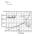
- FIG. 6 shows the torque characteristic curve that represents the dependency of the electrostatic driving torque (Te) upon the mirror tilt angle.
- the hinge spring characteristic curve that represents the elastic restoring force K ⁇ for a tilt angle ⁇ (where K is the stiffness of the hinge spring) is a straight line that passes through the origin and is tangent to the torque characteristic curve.
- the tilt angle at the point of contact ⁇ MAX is the maximum steering angle within the range of tilt angles in which stable angle positioning is possible, as will be explained hereinbelow.
- the torque characteristic curve intersects the hinge spring characteristic line at two points if the applied voltage is low. We denote, of these two points of intersection, the tilt angle of the intersection at the larger tilt angle as ⁇ H , and the tilt angle of the intersection at the smaller tilt angle as ⁇ L .
- the micromirror attains dynamic equilibrium at the tilt position ⁇ L .
- a rise of the applied voltage V results in an upward shift of the torque characteristic curve.
- the two intersection points approach each other with an increase in ⁇ L and a decrease in ⁇ H .
- Fig. 6 represents this situation.
- the tilt angle ⁇ MAX is thus the maximum value of ⁇ L , i.e., the maximum steering angle within the range of tilt angles in which stable angle positioning is possible.
- the maximum value ⁇ MAX of the mirror tilt angle for the applied voltage 150 V is 5.2 degrees.
- the maximum tilt angle of mirror frame 303 is of the same level when the stiffness of the hinge springs and the area and position of the electrodes are similarly set, and biaxial drive of the optical device for steering optical signals can thus be realized over the range of ⁇ 5.2 degrees.
- an analog beam-steering free-space optical switch is required to extend the range of mirror steering ⁇ MAX in order to be adaptive to a tendency toward scale-up of the switch while suppressing optical loss.
- the angular range ⁇ MAX for angular positioning of micromirror 203 and mirror frame 303 is limited by restrictions arising from the torque characteristics of the device and elastic characteristics of the parts. Control of the angular positions of micromirror 203 and mirror frame 303 is thus performed within a range of tilt angles limited by these restrictions.
- the electrostatic actuator in order to extend the range of micromirror steering of an analog beam-steering free-space optical switch, the electrostatic actuator must be designed to extend the maximum controllable tilt angle ⁇ MAx .
- the air gap must be increased to avoid electrostatic breakdown caused by contact between the micromirror and the electrode at a large tilt angle. Increasing the air gap while keeping the driving voltage fixed, however, lowers the torque characteristic curve and causes the obtainable maximum tilt angle to become smaller.
- the maximum controllable tilt angle ⁇ MAX can be extended if the stiffness of the hinge springs is designed to be soft. Reducing the stiffness of the hinge spring, however, brings about the risk of breaking during processing, complicates handling of the components, and further, reduces the response speed of the optical device and leads to switching delay.
- the invention adopts the basic construction described hereinbelow.
- the optical switch according to the invention is one for connecting and switching optical paths of a plurality of optical signals and includes a plurality of optical devices and electrostatic actuators for driving these devices: the optical device is pivotally borne so as to allow rotation around prescribed axes of rotation; and the electrostatic actuator includes a substrate that holds the optical device and a plurality of driving electrodes each assigned to rotate said optical device around one of said prescribed axes of rotation and mounted on the substrate.
- An electrostatic voltage when applied between the optical device and any one of the driving electrodes, generates an electrostatic driving torque for causing the optical device to tilt with respect to the substrate around an assigned axis of rotation. Control of the electrostatic driving torque allows control of the tilt of the optimal device around the assigned axis of rotation and changes the direction of reflection of optical signals.
- an assigned axis of rotation refers to one of the prescribed axes of rotation around which the driving electrode of interest is assigned to rotate the optical device.
- each of the plurality of driving electrodes is formed in a shape in which the electrode width of a prescribed end portion remote from the electrode axis of the driving electrode of interest narrows with progression away from the electrode axis.
- the electrode axis refers to an orthogonal projection of the assigned axis of rotation onto the substrate surface.
- the plurality of driving electrodes is arranged in a radial pattern with respect to the electrode center, and each of the plurality of driving electrodes is formed in a shape in which the electrode width of a prescribed outer portion thereof with respect to the electrode center narrows with progression toward the outside.
- the electrode center is the orthogonal projection of the center of rotation onto the substrate surface and the center of rotation refers to a point of interception of the prescribed axes of rotation.
- the width of the electrode thus decreases with progression toward the outer circumference of the driving electrodes, the electrostatic driving torque that is applied to the outer circumferential portion of the micromirror is reduced compared to the prior art even when the same electrostatic driving voltage is applied.
- a decrease in the electrostatic attractive force caused by narrowing of the width of the driving electrode compensates for an increase in the electrostatic attractive force caused by an increase in the tilt angle, a steep rise of the electrostatic driving torque in a large steering angle region is relaxed.
- the optical device has a micromirror, a mirror frame arranged to surround the circumference of the micromirror, and a frame arranged to surround the circumference of the mirror frame.
- the micromirror is pivotally borne by the mirror frame such that it can rotate around a first rotational axis and that an elastic restoring force acts against this rotation.
- the mirror frame is also pivotally borne by the frame such that the mirror frame can rotate around a second rotational axis and that an elastic restoring force acts against this rotation.
- the first rotational axis and the second rotational axis intersect on a plane parallel to the substrate. This point of intersection therefore forms the center of rotation of the optical device.
- the plurality of driving electrodes can include a first electrode pair and a second electrode pair: a first electrode pair generates electrostatic driving torque far causing the micromirror to rotate around the first rotational axis; and a second electrode pair generates electrostatic driving torque for causing the mirror frame to rotate around the second rotational axis.
- the two electrodes of the first electrode pair are arranged on both sides of a first orthogonal plane and the two electrodes of the second electrode pair on both sides of a second orthogonal plane.
- the first orthogonal plane includes the first rotational axis and is perpendicular to the substrate.
- the second orthogonal plane includes the second rotational axis and is perpendicular to the substrate.
- the first and the second rotational axes are arranged orthogonal to each other.
- each of the driving electrodes may be shaped such that the electrode width of a prescribed inner portion with respect to the electrode center narrows with progression toward the inside.
- the pair of electrodes for rotating the micromirror and that for rotating the mirror frame can each be extended into the vicinity of the electrode center without causing geometric interference.
- a large electrostatic driving torque can be generated with a low driving voltage, and the electrostatic driving torque can be set to a high value in the region of small steering angles.
- the first optical switch can include an embodiment in which each of the driving electrodes is formed in a shape both such that the electrode width of a prescribed inner portion with respect to the electrode center narrows with radially inward progression and also that the electrode width of a prescribed outer portion with respect to the electrode center narrows with radially outward progression.
- the electrostatic driving torque characteristic curve shifts upward as a whole because the driving electrodes are extended toward the inside with respect to the electrode center, but, on the other hand, the electrostatic driving torque characteristic curve shifts downward because the electrode width of the driving electrodes narrows with radially outward progression with respect to the electrode center. This downward shift is more conspicuous with larger tilt angles. Accordingly, in comparison with prior art, the shape of the driving electrodes produces an electrostatic driving torque characteristic in which the electrostatic driving torque characteristic curve is shifted upward in the tilt-angle range where the tilt angle is small and downward in the tilt-angle range where the tilt angle is large. Thus, this electrostatic driving torque characteristic curve exhibits a characteristic that rises more gradually with increase in the tilt angle than the characteristic curve of the prior art.
- the range, within which the tilt angle can be controlled extends, i.e., the maximum controllable tilt angle increases, as described below:
- the electrostatic driving torque characteristic curve for the tilt angle of the present embodiment is shifted up from that of the prior art.
- the slope or gradient of a tangent line drawn from the origin to the electrostatic driving torque characteristic curve is larger than the slope of a tangent line in prior art; generally, when a fixed voltage is applied between the micromirror and driving electrodes to generate an electrostatic driving torque, this increases monotonically with increase in the tilt angle of the micromirror, however, the rate of change of this torque increases as the tilt angle increases (i.e., the electrostatic driving torque characteristic curve rises more sharply with increase in the tilt angle); accordingly, even if the gradient of the electrostatic driving torque characteristic curve of the present embodiment were exactly the same as that of the prior art, the tilt angle coordinates in the point of contact of the tangent line would be larger in the embodiment than in prior art, because the gradient of the torque characteristic curve at the point of contact of the tangent line is larger in this embodiment
- This embodiment has the advantage of a shorter response time than the prior art technique as well, because the slope of the tangent line, drawn from the origin to the electrostatic driving torque characteristic curve, corresponds to an elastic constant of the elastic member. Since the slope of the tangent line in larger in the embodiment than in the prior art, the embodiment enables to employ an elastic member of a high elastic constant, which causes a short response time, only.
- the driving electrodes can each be in a rhombus shape.
- the shape of each driving electrode may also be an oval shape having its major axis aligned with a radial direction relative to the electrode center.
- the second embodiment of the optical switch of the invention is characterized by: a first electrode pair that is a pair of circular-segment electrodes of the same size each having a central angle of approximately 180 degrees, the two electrodes being arranged concentric with the electrode center and confronting each other on both sides of a first orthogonal plane; and a second electrode pair that is a pair of concentric circular-segment electrodes of the same size having a central angle of approximately 180 degrees, the two electrodes are arranged concentric with the electrode center and confront each other on both sides of a second orthogonal plane; wherein the first electrode pair is arranged concentric with and inside the second electrode pair with respect to the electrode center.
- the first orthogonal plane includes the first rotational axis and extends perpendicular to the substrate surface
- the second orthogonal plane includes the second rotational axis and extends perpendicular to the substrate surface
- Wiring for supplying power to each electrode of the first electrode pair is provided in the gap that extends between the confronting ends of the second electrode pair.
- the micromirror of the optical device is preferably pivotally borne by the first hinge springs on the first rotational axis, and the mirror frame is preferably pivotally borne by the second hinge springs on the second rotational axis.
- the tilt stiffness of the second hinge springs is set stiffer than that of first hinge springs.
- the ratio of the tilt stiffness of the first hinge springs to that of the second hinge springs is preferably set to equal the ratio of the electrostatic driving torque to be generated by the first electrode pair to the electrostatic driving torque to be generated by the second pair when the same driving voltage is applied between the first and second driving electrode pairs and the micromirror.
- An optical switch is formed by arranging optical devices and electrostatic actuators depending on the number of input and output ports in array form.
- the above-described electrode configuration of an optical switch enables one pair of electrodes for rotating a micromirror and one pair for rotating a mirror frame to be efficiently arranged to cover the largest possible electrode area in an effective electrode region on the substrate that confronts the micromirror.
- the circular-segment electrode shape in which the essential electrode width narrows toward an outward direction with respect to the electrode center, i.e., toward the outer circumference of the above-described effective electrode region, allows the electrostatic driving torque to be set to high values in the region of small steering angles, as with the optical switch of the above-described first embodiment; and further, enables suppression of too strong electrostatic force generated at tilt angle positions at which the micromirror and the electrodes approach, thereby allowing a suppression of steep rises in electrostatic driving torque.
- the tilt stiffness of the hinge springs for pivotally bearing the mirror frame is set to be stiffer than that of the hinge springs for pivotally bearing the micromirror in order to realize proper performance of steering control of the micromirror.
- this embodiment enables an extension of the range of the steering angle that is controllable under low-voltage drive while improving the stiffness of the hinge springs of the pivotal bearing portions, thereby enabling to provide an accurate optical switch applicable to large-scale switches.
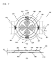
- FIG. 7 in which is shown the configuration of an optical switch of a first embodiment, FIG. 7(a) showing a plan view and FIG. 7(b) showing a side view.
- FIG. 8 is a plan view and Fig. 9 is a graph as given above.
- An optical switch comprises an optical device and an electrostatic actuator for driving this optical device, and performs connecting and switching of a plurality of optical signal paths.
- the optical device is borne so as to allow rotation around one or more directions.
- the electrostatic actuator comprises the substrate that holds the optical device and driving electrodes secured on the substrate.
- the driving electrodes are arranged radially around the electrode center. Each electrode is formed in a shape such that the electrode width of a prescribed outer portion decreases with progression in an outward direction from the electrode center.
- the optical device is pivotally borne so as to allow rotation around two directions, i.e., around two intersecting rotational axes A1 and A2.
- the intersection of the two rotational axes is referred to as the center of rotation.
- the orthogonal projection of the center of rotation onto the substrate surface is referred to as the electrode center (EC).
- the plane that is perpendicular to the substrate surface and that contains rotational axis A1 is referred to as a first orthogonal plane
- the plane that is perpendicular to the substrate surface and that contains rotational axis A2 is referred to as a second orthogonal plane.
- the lines on which the first and second orthogonal plane intersect with the substrate surface are referred to as the first and second orthogonal projection axes, respectively.
- the optical device includes micromirror 201, mirror frame 301 arranged to surround the circumference of micromirror 201, and frame 701 arranged to surround the circumference of mirror frame 301.
- Micromirror 201 is pivotally borne by mirror frame 301 by means of a pair of first hinge springs 501, and is elastically borne such that micromirror 201 can rotate around rotational axis A1 (RY direction) of FIG. 7.
- Mirror frame 301 is elastically and pivotally borne by frame 701 by means of a pair of second hinge springs 601 such that mirror frame 301 can rotate around rotational axis A2 (RX direction), which is orthogonal to rotational axis A1 of the micromirror.
- the electrostatic actuator comprises substrate 1101 that holds the optical device and driving electrodes 901 and 1001 mounted on substrate 1101.
- Driving electrode 901 has two driving electrodes formed on both sides of the first orthogonal plane.
- Driving electrode 1001 has two driving electrodes formed on both sides of the second orthogonal plane.
- Prescribed outer portions of driving electrodes 901 and 1001 as viewed from the electrode center are formed such that the electrode width W narrows with progression outward from the electrode center (refer to portion a of FIG. 8(a) and portion a1 of FIG. 8(b)).
- the inner portions of driving electrodes 901 and 1001 as viewed from the electrode center are formed such that electrode width W narrows with progression toward the center of rotation EC of the optical device.
- the above-described two sets of driving electrodes are arranged on the substrate within the areas of orthogonal projection of the micromirror.
- the pair of driving electrodes 901 (hereinbelow referred to as the first electrode pair) is formed to lie on both sides of the first orthogonal plane, whereby the electrostatic force generated by the first pair generates a torque that causes the micromirror to rotate around rotational axis A1.
- driving electrode 1001 (hereinbelow referred to as the second electrode pair) is formed to lie on both sides of the second orthogonal plane, whereby an electrostatic force generated by the second electrode pair generates a torque causing the micromirror to rotate around rotational axis A2 through mirror frame 301.
- Rotational axis A1 and rotational axis A2 are established in a mutually orthogonal relation, and the two electrode pairs 901 and 1001 can therefore generate torque around any rotational axis within the plane that contains rotational axis A1 and rotational axis A2 (biaxial drive).
- a prescribed electrode separation (air gap) 22 is provided between the driving electrodes and the center of rotation of the optical device, the optical device being grounded.
- Application of a driving voltage to each of the electrode pairs generates electrostatic attraction between the grounded optical device and the driving electrodes, and causes micromirror 201 and mirror frame 301 to rotate around each rotational axis, thereby reflecting an incident optical signal toward any direction.
- each driving electrode is formed in a novel shape.
- the driving electrode shown in FIG. 7(a) takes the shape such that electrode width W of the inner portions as seen from electrode center (the portions that are close to the electrode center) decreases with inward progression toward the electrode center, while at the same time, the electrode width W of the outer portions decreases with outward progression from the electrode center.
- the driving electrodes of FIG. 7(a) are thus formed in a rhombus shape.
- FIG. 8 shows other embodiments of the electrode shape.
- FIG. 8(a) shows an equilateral rhombus-shaped electrode
- FIG. 8(b) shows an electrode in which the position of maximum electrode width of the rhombus-shaped electrode has been shifted outward (in the direction away from the electrode center) from that of the rhombus-shaped electrode of FIG. 8(a) (a1 ⁇ a2).
- FIG. 8 (c) shows an electrode in which the shape has been set as an oval.
- Each electrode pair of this shape is formed such that the major axis coincides with the orthogonal projection axis.
- each electrode is formed such that the width decreases with progression toward the center, while at the same time the width decreases with progression outward relative to the center. The same effect can therefore be achieved regarding the electrostatic driving torque characteristic as with the above-described rhombus-shaped electrodes. Since the dimensions of the major axis and minor axis are optimized according to the design parameters of the optical device and electrostatic actuator, the shape of the electrodes may in some cases be set as a circle.
- the shape can be optimally designed in accordance with the limits of the design parameters of the optical device or with the demands of the driving voltage circuits.
- Forming the electrodes such that the electrode width of portions close to the electrode center decreases in this way allows an extension of first pair 901 and second pair 1001 as far as the vicinity of the center without causing geometrical interference.
- the areas of the electrodes can be increased, and higher torque can be generated for the same mirror tilt angle than in the prior art, at the same applied voltage.
- the inward extension of the electrode areas causes an upward shift of the electrostatic driving torque-versus mirror tilt angle characteristic curve .
- FIG. 9 is a graph showing the driving torque characteristic of the optical switch in the first embodiment of the invention, FIG. 9(a) showing the electrostatic driving electrodes of the prior art and FIG. 9(b) showing the rhombus-shaped electrostatic driving electrodes of this embodiment.
- FIG. 9(c) shows the results of calculating the electrostatic driving torque characteristic versus mirror tilt angle ⁇ .
- the broken-line in the figure represents the electrostatic driving torque characteristic curve when using the electrostatic driving electrodes of the prior art shown in FIG 9(a), and the solid-line curve represents the electrostatic driving torque characteristic curve when using the rhombus-shaped electrostatic driving electrodes of FIG. 9(b).
- the slope (or gradient) of each of these lines represents the stiffness of the hinge spring.
- the electrode portion that extends as far as the vicinity of the electrode center produces an additive electric field E' in the vicinity of rotational axes A1 and A2 (x ⁇ L).
- the upward arrow inserted in the small ⁇ region represents the electrostatic torque increment caused by the additive electrostatic field E'.
- the width W of the driving electrodes gradually narrows with progression toward the outside as viewed from the electrode center, as previously described. This shape results in a circumferential area of an electrode smaller than that of the prior art, and the electrostatic driving torque therefore lowers. However, the rate of decrease in the electrostatic driving torque increases as the mirror tilt angle ⁇ increases.
- the electrode width W set so as to decrease with outward progression thus suppresses a sharp rise in the electrostatic driving torque-versus-tilt angle characteristic even in the region of large steering angles where the edge of the mirror approaches the driving electrodes and electrode separation (air gap) 22 becomes small.
- the initial driving torque can be set high in the region of small steering angles at a start of driving.
- the driving torque characteristic for the driving electrodes of this embodiment is as follows:
- the initial torque of the movable mirror rises (upward arrow in Fig. 9 (c)), and moreover, a rise in the electrostatic driving torque plotted against the tilt angle are suppressed (downward arrow in Fig. 9 (c)).
- the embodiment allows the range of the steering angle (the tilt angle at the contact point of a tangent from the origin and the driving torque curve) for which stable positioning is possible to be extended.
- the hinge spring stiffness tilt stiffness
- an optical switch can be provided in which the mirror steering angle is extended without reducing the response speed of the movable mirror.
- a compact, low-cost, highly reliable, and high-speed optical switch that is suitable for large-scale applications can therefore be provided.
- the optical switch in the embodiment is amenable to processing in which MEMS technology is applied.
- a multiplicity of optical switches can be arranged in matrix form on a silicon wafer and modularized (refer to the prior-art example of FIG. 2(b)); and input/output fiber arrays can be combined with collimation lens arrays to constitute a large-scale optical switch module (refer to the prior-art example of FIG. 2(a)).
- an electrostatic actuator was constructed by affixing driving electrodes to the substrate and grounding the optical device in the previously described embodiment, a construction may also be adopted in which the driving electrodes are arranged on the optical device and the substrate is grounded.
- the structure of the hinge spring portion in the embodiment was set to a serpentine shape as shown in the prior-art example, any structure capable of obtaining the prescribed stiffness may be employed.
- optical switch of this embodiment is directed to connecting and switching optical paths of a plurality of optical signals and is provided with optical devices and electrostatic actuators driving these optical devices.
- the optical device is provided with: a circular micromirror, a substantially concentric circular mirror frame arranged to surround the circumference of the micromirror, and a frame arranged to surround the circumference of the mirror frame.
- the rotational axis of the micromirror (hereinbelow referred to as rotational axis A1) passes through a diameter of micromirror 202.
- the rotational axis of the mirror frame (hereinbelow referred to as rotational axis A2) passes through a diameter of the mirror frame that is orthogonal to rotational axis A1.
- the micromirror is pivotally borne by the mirror frame by means of first hinge springs, and the mirror frame is pivotally borne by the frame by means of second hinge springs such that the mirror frame can rotate around an axis orthogonal to rotational axis A1 of the micromirror.
- the electrostatic actuator is provided with the substrate that holds the optical device and driving electrodes affixed on the substrate.
- the driving electrodes are provided with a first electrode pair causing the micromirror to rotate and a second electrode pair causing the mirror frame to rotate.
- the first electrode pair is constituted by a pair of circular-segment electrodes each a central angle of approximately 180 degrees and having the same size.
- the two end edges of each of the circular-segment electrodes of the first electrode pair are arranged to confront the two end edges of the other circular-segment electrode on both sides of the first orthogonal plane.
- the second electrode pair is a pair of concentric circular-segment electrodes each having a central angle of approximately 180 degrees, and the two end edges of each of the concentric circular-segment electrodes are arranged to confront the two end edges of the other concentric circular-segment electrode on both sides of the second orthogonal plane.
- the first electrode pair is located radially inward of the second electrode pair with respect to the electrode center.
- the second electrode pair is thus arranged in a position that is rotated 90 degrees with respect to the first electrode pair.
- FIG. 10(a) is a plan view of the optical switch that represents the present embodiment
- FIG. 10(b) and (c) are plan views showing the shapes of the electrodes in this embodiment.
- the optical switch of this embodiment is also constituted by an optical device and an electrostatic actuator for driving the optical device, and performs connection and switching of optical paths of a plurality of optical signals.
- the constitution of the optical device is similar to that of the first embodiment, and is provided with micromirror 202, mirror frame 302, and frame 702.
- Mirror frame 302 is arranged to surround the circumference of micromirror 202.
- Frame 702 is arranged to surround the circumference of mirror frame 302.
- Micromirror 202 is pivotally borne by mirror frame 302 by means of first hinge springs 502.
- Mirror frame 302 is pivotally borne by frame 702 by means of second hinge springs 602 such that mirror frame 302 can rotate around rotational axis A2 orthogonal to rotational axis A1 of micromirror 202.
- the electrostatic actuator is provided with the substrate that holds the optical device and driving electrodes 902 and 1002 affixed onto the substrate.
- the driving electrodes are constituted by first electrode pair 902 for rotating micromirror 202 and second electrode pair 1002 for rotating mirror frame 302.
- the first pair is arranged such that the two end edges of each of the pair of circular-segment electrodes 902, each having a central angle of approximately 180 degrees, confront the two end surfaces of the other circular-segment electrode on both sides of the first orthogonal plane.
- the second pair is arranged with each of the pair of concentric circular-segment electrodes 1002, each having a central angle of approximately 180 degrees, confronting each other on both sides of the second orthogonal plane, which contains rotational axis A2 of mirror frame 302.
- First electrode pair 902 is arranged surrounded by and inward of second pair 1002 as viewed from the electrode center. Second pair 1002 is thus arranged at a position that is rotated 90 degrees with respect to first pair 902.
- electrode wiring lines 2301 of the two circular-segment electrodes of first pair 902 are led to the external of the substrate such that the lines pass through gap G between the confronting edges of the two concentric circular-segment electrodes of second pair 1002 (see FIG. 10(c)).
- a prescribed electrode separation is provided between driving electrodes 902 and 1002 and the optical device.
- the application of a voltage to either electrode of each of the first and second electrode pairs generates electrostatic force (attraction) and thus steers the movable mirror to perform steering of an optical signal.
- tilt stiffness Kh2 of second hinge springs 602 that pivotally bear mirror frame 302 is set to be larger than the tilt stiffness Kh1 of first hinge springs 502 that pivotally bear micromirror 202.
- This setting is for compensating for the difference in electrostatic force caused by the difference in the areas of the electrodes and thereby improving the control of the micromirror.
- the ratio of Kh1 to Kh2 is set to equal the ratio of the electrostatic torque generated by first electrode 902 to the electrostatic torque generated by second electrode 1002 when the same voltage is applied.
- this electrode structure and hinge spring stiffness allows the electrodes to drive the micromirror and the electrodes to drive the mirror frame to be efficiently arranged in the largest possible area of the electrode within the effective region of the substrate that confronts the micromirror. Furthermore, narrowing the essential electrode width (the electrode width that generates electrostatic driving force) with outward progression relative to the electrode center allows suppression of a steep rise in the electrostatic driving torque characteristic curve plotted against a tilt angle, as in the first embodiment. As a result, the range of the steering angle in which control is possible at low-voltage drive can be extended, and an optical switch applicable to a large-scale switch can be provided.
- the tilt stiffness of the hinge spring portion that bears the mirror frame is set to a larger stiffness than that of the micromirror depending on the difference in electrostatic driving torque between the micromirror and mirror frame.
- optical device and driving electrodes in the optical switch of the embodiment are also amenable to processing using MEMS technology.
- a multiplicity of optical switches may be arranged two-dimensionally in matrix form on a silicon chip and combined with a fiber array and lens array to construct a large-scale optical switch module.
- the driving electrodes are mounted on the substrate and the optical device is grounded.
- the same results can be obtained when a construction is adopted in which the driving electrodes are arranged on the optical device and the substrate is grounded.
- the structure of the hinge spring portion is established as a serpentine shape in the present embodiment, this construction is not particularly specified, and any structure that can obtain the prescribed stiffness may be employed.
- the present invention has the following technical merits:
- the shape of electrodes of the electrostatic actuator to drive the micromirror is set such that the electrode width narrows with progression toward the electrode center, and at the same time, the electrode width also narrows with outward progression relative to the electrode center.
- the shape of the electrodes of the electrostatic actuator for driving the micromirror is provided with two circular-segment electrodes each having a central angle of approximately 180 degrees and placed in mutual confrontation.
- the electrode pair for driving the micromirror is arranged toward the electrode center, and the electrode pair for driving the mirror frame is arranged outside the electrode pair for driving the micromirror and rotated 90 degrees with respect to the electrode pair for driving the micromirror.
- the tilt stiffness of the elastic members (hinge spring portion) that bear the mirror frame is set larger than the tilt stiffness of the elastic members (hinge spring portion) that bear the micromirror.
- This configuration allows an improvement of the driving torque characteristic of the micromirror as well as an improvement of the mirror control, and allows an extension of the range of controllable steering angles at low-voltage drive.
- the invention offers an advantage of providing an accurate optical switch suitable for applications to large-scale optical communication.
Landscapes
- Physics & Mathematics (AREA)
- Engineering & Computer Science (AREA)
- Computer Hardware Design (AREA)
- Microelectronics & Electronic Packaging (AREA)
- General Physics & Mathematics (AREA)
- Optics & Photonics (AREA)
- Mechanical Light Control Or Optical Switches (AREA)
- Micromachines (AREA)
Applications Claiming Priority (2)
| Application Number | Priority Date | Filing Date | Title |
|---|---|---|---|
| JP2001218447A JP3722021B2 (ja) | 2001-07-18 | 2001-07-18 | 光スイッチ |
| JP2001218447 | 2001-07-18 |
Publications (3)
| Publication Number | Publication Date |
|---|---|
| EP1278083A2 true EP1278083A2 (fr) | 2003-01-22 |
| EP1278083A3 EP1278083A3 (fr) | 2004-09-22 |
| EP1278083B1 EP1278083B1 (fr) | 2007-05-30 |
Family
ID=19052624
Family Applications (1)
| Application Number | Title | Priority Date | Filing Date |
|---|---|---|---|
| EP02090242A Expired - Fee Related EP1278083B1 (fr) | 2001-07-18 | 2002-07-10 | Commutateur optique |
Country Status (5)
| Country | Link |
|---|---|
| US (1) | US6795603B2 (fr) |
| EP (1) | EP1278083B1 (fr) |
| JP (1) | JP3722021B2 (fr) |
| CN (1) | CN1178083C (fr) |
| DE (1) | DE60220344T2 (fr) |
Families Citing this family (30)
| Publication number | Priority date | Publication date | Assignee | Title |
|---|---|---|---|---|
| US7050669B2 (en) * | 2001-04-30 | 2006-05-23 | Trex Enterprises Corp. | Optical cross connect switch with axial alignment beam |
| KR100819299B1 (ko) * | 2002-08-09 | 2008-04-03 | 삼성전자주식회사 | 장식용 벨트를 구비하는 휴대용 무선 단말기 |
| US7019434B2 (en) * | 2002-11-08 | 2006-03-28 | Iris Ao, Inc. | Deformable mirror method and apparatus including bimorph flexures and integrated drive |
| US20040160118A1 (en) * | 2002-11-08 | 2004-08-19 | Knollenberg Clifford F. | Actuator apparatus and method for improved deflection characteristics |
| WO2004074903A1 (fr) * | 2003-02-19 | 2004-09-02 | Intellimicrons Co., Ltd. | Miroir de balayage avec deux degres de liberte et procede de fabrication de ce miroir |
| JP4360923B2 (ja) | 2004-01-20 | 2009-11-11 | Hoya株式会社 | マイクロミラー装置 |
| JP4227531B2 (ja) * | 2004-01-27 | 2009-02-18 | Hoya株式会社 | ヒンジ構造 |
| US7160753B2 (en) * | 2004-03-16 | 2007-01-09 | Voxtel, Inc. | Silicon-on-insulator active pixel sensors |
| JP4627627B2 (ja) * | 2004-03-31 | 2011-02-09 | 富士通株式会社 | マイクロミラー素子および光スイッチ |
| US7356880B2 (en) * | 2004-07-26 | 2008-04-15 | Pentax Corporation | Hinge structure of micromirror device |
| JP2006053396A (ja) | 2004-08-12 | 2006-02-23 | Tohoku Univ | 駆動機構、および該機構を備えたマイクロミラー装置 |
| WO2006046592A1 (fr) | 2004-10-29 | 2006-05-04 | Pentax Corporation | Dispositif scanneur de lumière petit modèle |
| US8319307B1 (en) | 2004-11-19 | 2012-11-27 | Voxtel, Inc. | Active pixel sensors with variable threshold reset |
| CN100451725C (zh) * | 2005-01-05 | 2009-01-14 | 日本电信电话株式会社 | 反射镜器件、反射镜阵列、光开关及其制造方法 |
| JP4550653B2 (ja) * | 2005-04-15 | 2010-09-22 | 富士通株式会社 | マイクロ可動素子および光スイッチング装置 |
| US20070188582A1 (en) * | 2006-02-15 | 2007-08-16 | Honeywell International Inc. | Electrostatic actuator with charge control surface |
| CA2747115C (fr) * | 2006-07-27 | 2014-06-17 | Nippon Telegraph And Telephone Corporation | Dispositif de commande de miroir |
| JP5151944B2 (ja) | 2008-12-09 | 2013-02-27 | セイコーエプソン株式会社 | 光フィルタ及びそれを備えた光モジュール |
| CN102820916A (zh) * | 2011-06-10 | 2012-12-12 | 辽宁省电力有限公司大连供电公司 | 光信号传输通断器 |
| JP2014059497A (ja) * | 2012-09-19 | 2014-04-03 | Seiko Epson Corp | 波長可変干渉フィルター、光学フィルターデバイス、光学モジュール、電子機器、及びmemsデバイス |
| DE102013217111A1 (de) * | 2013-08-28 | 2015-03-19 | Robert Bosch Gmbh | Mikromechanisches Bauteil und Verfahren zur Herstellung eines mikromechanischen Bauteils |
| WO2015099747A1 (fr) * | 2013-12-26 | 2015-07-02 | Empire Technology Development, Llc | Micro-miroir défocalisé permettant d'afficher des images à réalité augmentée |
| US9341790B2 (en) * | 2014-03-10 | 2016-05-17 | Huawei Technologies Co., Ltd. | Device and method for micro-electro-mechanical-system photonic switch |
| CN104932098B (zh) | 2015-07-17 | 2017-04-05 | 京东方科技集团股份有限公司 | 微镜阵列和应用其的背光模组及显示装置 |
| US11163152B2 (en) | 2017-08-02 | 2021-11-02 | United States Of America As Represented By The Secretary Of The Air Force | MEMS electrothermal actuator for large angle beamsteering |
| US11535511B2 (en) | 2017-08-02 | 2022-12-27 | United States Of America As Represented By The Secretary Of The Air Force | Post-processing techniques on mems foundry fabricated devices for large angle beamsteering |
| CN111342809B (zh) * | 2018-12-18 | 2023-10-24 | 天津大学 | 提高抗静电击穿能力的谐振器及滤波器和电子设备 |
| US11774785B2 (en) | 2020-03-30 | 2023-10-03 | British Telecommunications Public Limited Company | Optical limiter and method for limiting radiant flux |
| WO2021197779A1 (fr) | 2020-03-30 | 2021-10-07 | British Telecommunications Public Limited Company | Interrupteur optique, procédé et système de routage optique |
| CN112558230B (zh) * | 2020-12-07 | 2022-10-21 | 中国科学院合肥物质科学研究院 | 一种多通道分时复测光耦合装置与使用方法 |
Citations (3)
| Publication number | Priority date | Publication date | Assignee | Title |
|---|---|---|---|---|
| US5408355A (en) * | 1991-10-30 | 1995-04-18 | Labor Dr. Hans Steinbichler | Micromechanical transducer |
| US6201631B1 (en) * | 1999-10-08 | 2001-03-13 | Lucent Technologies Inc. | Process for fabricating an optical mirror array |
| EP1223453A2 (fr) * | 2001-01-05 | 2002-07-17 | Agere Systems Guardian Corporation | Dispositif micro électro-mécanique actionné électrostatiquement |
Family Cites Families (15)
| Publication number | Priority date | Publication date | Assignee | Title |
|---|---|---|---|---|
| US5661591A (en) * | 1995-09-29 | 1997-08-26 | Texas Instruments Incorporated | Optical switch having an analog beam for steering light |
| US5867297A (en) * | 1997-02-07 | 1999-02-02 | The Regents Of The University Of California | Apparatus and method for optical scanning with an oscillatory microelectromechanical system |
| US6253001B1 (en) * | 2000-01-20 | 2001-06-26 | Agilent Technologies, Inc. | Optical switches using dual axis micromirrors |
| US6585383B2 (en) * | 2000-05-18 | 2003-07-01 | Calient Networks, Inc. | Micromachined apparatus for improved reflection of light |
| US6483962B1 (en) * | 2000-05-24 | 2002-11-19 | Vlad J. Novotny | Optical cross connect switching array system with optical feedback |
| US6318871B1 (en) * | 2000-06-09 | 2001-11-20 | C Speed Corporation | Optical mirror system with multi-axis rotational control |
| US6337760B1 (en) * | 2000-07-17 | 2002-01-08 | Reflectivity, Inc. | Encapsulated multi-directional light beam steering device |
| JP2002214546A (ja) * | 2000-11-15 | 2002-07-31 | Oki Electric Ind Co Ltd | 光スイッチ |
| US6681063B1 (en) * | 2000-11-16 | 2004-01-20 | Computer Optics Inc | Low voltage micro-mirror array light beam switch |
| US6597827B1 (en) * | 2001-01-10 | 2003-07-22 | Tellium, Inc. | Voltage reduction in integrated control systems of mirrors |
| KR100403812B1 (ko) * | 2001-06-23 | 2003-10-30 | 삼성전자주식회사 | 마이크로 액츄에이터 |
| US6657759B2 (en) * | 2001-07-03 | 2003-12-02 | Pts Corporation | Bistable micromirror with contactless stops |
| US6701037B2 (en) * | 2001-07-03 | 2004-03-02 | Pts Corporation | MEMS-based noncontacting free-space optical switch |
| US6873447B2 (en) * | 2001-07-03 | 2005-03-29 | Pts Corporation | Two-dimensional free-space optical wavelength routing element based on stepwise controlled tilting mirrors |
| US6717325B2 (en) * | 2002-03-06 | 2004-04-06 | Glimmerglass Networks, Inc. | Method and apparatus for actuation of a two-axis MEMS device using three actuation elements |
-
2001
- 2001-07-18 JP JP2001218447A patent/JP3722021B2/ja not_active Expired - Fee Related
-
2002
- 2002-07-10 EP EP02090242A patent/EP1278083B1/fr not_active Expired - Fee Related
- 2002-07-10 DE DE60220344T patent/DE60220344T2/de not_active Expired - Lifetime
- 2002-07-16 US US10/195,741 patent/US6795603B2/en not_active Expired - Fee Related
- 2002-07-18 CN CNB021263124A patent/CN1178083C/zh not_active Expired - Fee Related
Patent Citations (3)
| Publication number | Priority date | Publication date | Assignee | Title |
|---|---|---|---|---|
| US5408355A (en) * | 1991-10-30 | 1995-04-18 | Labor Dr. Hans Steinbichler | Micromechanical transducer |
| US6201631B1 (en) * | 1999-10-08 | 2001-03-13 | Lucent Technologies Inc. | Process for fabricating an optical mirror array |
| EP1223453A2 (fr) * | 2001-01-05 | 2002-07-17 | Agere Systems Guardian Corporation | Dispositif micro électro-mécanique actionné électrostatiquement |
Non-Patent Citations (3)
| Title |
|---|
| AKSYUK V A ET AL: "LUCENT MICROSTARTM MICROMIRROR ARRAY TECHNOLOGY FOR LARGE OPTICAL CROSSCONNECTS" PROCEEDINGS OF THE SPIE, SPIE, BELLINGHAM, VA, US, vol. 4178, 2000, pages 320-324, XP001038165 ISSN: 0277-786X * |
| BURNS D M ET AL: "Investigation of the maximum optical power rating for a micro-electro-mechanical device" 1997 INTERNATIONAL CONFERENCE ON SOLID-STATE SENSORS AND ACTUATORS. DIGEST OF TECHNICAL PAPERS. TRANSDUCERS 97. CHICAGO, IL, JUNE 16 - 19, 1997. SESSIONS 3A1 - 4D3. PAPERS NO. 3A1.01 - 4D3.14P, INTERNATIONAL CONFERENCE ON SOLID-STATE SENSORS AND ACTU, vol. VOL. 2, 16 June 1997 (1997-06-16), pages 335-338, XP010240478 ISBN: 0-7803-3829-4 * |
| DOTZEL W ET AL: "Silicon mirrors and micromirror arrays for spatial laser beam modulation" 1997 INTERNATIONAL CONFERENCE ON SOLID-STATE SENSORS AND ACTUATORS. DIGEST OF TECHNICAL PAPERS. TRANSDUCERS 97. CHICAGO, IL, JUNE 16 - 19, 1997. SESSIONS 3A1 - 4D3. PAPERS NO. 3A1.01 - 4D3.14P, INTERNATIONAL CONFERENCE ON SOLID-STATE SENSORS AND ACTU, vol. VOL. 2, 16 June 1997 (1997-06-16), pages 81-84, XP010240413 ISBN: 0-7803-3829-4 * |
Also Published As
| Publication number | Publication date |
|---|---|
| EP1278083A3 (fr) | 2004-09-22 |
| EP1278083B1 (fr) | 2007-05-30 |
| US20030016906A1 (en) | 2003-01-23 |
| JP2003029172A (ja) | 2003-01-29 |
| JP3722021B2 (ja) | 2005-11-30 |
| DE60220344T2 (de) | 2008-01-24 |
| CN1178083C (zh) | 2004-12-01 |
| CN1397816A (zh) | 2003-02-19 |
| US6795603B2 (en) | 2004-09-21 |
| DE60220344D1 (de) | 2007-07-12 |
Similar Documents
| Publication | Publication Date | Title |
|---|---|---|
| US6795603B2 (en) | Optical switch | |
| Aksyuk et al. | Beam-steering micromirrors for large optical cross-connects | |
| US6859580B2 (en) | Systems and methods for overcoming stiction using a lever | |
| US6657759B2 (en) | Bistable micromirror with contactless stops | |
| US7126250B2 (en) | Apparatus comprising an array of tightly spaced rotatable optical elements with two axes of rotation | |
| US6360033B1 (en) | Optical switch incorporating therein shallow arch leaf springs | |
| US7529444B2 (en) | Optical steering element and method | |
| US7030537B2 (en) | Movable MEMS-based noncontacting device | |
| WO2003014784A2 (fr) | Dispositifs a miroirs mecaniques micro-electriques a taux de remplissage lineaire de miroir eleve | |
| WO2002001275A2 (fr) | Commutateur optique | |
| US6816640B2 (en) | Optical add drop multiplexer | |
| US6614581B2 (en) | Methods and apparatus for providing a multi-stop micromirror | |
| US6735004B1 (en) | Rotatable counterbalanced actuator | |
| KR100370079B1 (ko) | 마이크로미러 어레이와 그 제조방법 | |
| EP1099966B1 (fr) | Commutateur optique à micromiroir | |
| Takahashi et al. | A Silicon Micromachined $ f $-$\theta $ Microlens Scanner Array by Double-Deck Device Design Technique | |
| EP1205781B1 (fr) | Multiplexeur optique d'insertion/extraction | |
| US6907155B2 (en) | Three-dimensional optical switch with annular input-output ports | |
| KR20020068773A (ko) | 초미세전기기계시스템을 이용한 자유 공간 광스위치용박막 미소거울어레이의 구조와 그의 제조방법, 그리고이를 이용한 다차원 광스위칭 방식 | |
| US7079726B2 (en) | Microelectromechanical optical switch using bendable fibers to direct light signals | |
| Kim et al. | Performance of large scale MEMS-based optical crossconnect switches | |
| KR20020071206A (ko) | 다상 구동 전압에 의하여 구동되는 다수의 회전축을가지는 광파장 스위치 |
Legal Events
| Date | Code | Title | Description |
|---|---|---|---|
| PUAI | Public reference made under article 153(3) epc to a published international application that has entered the european phase |
Free format text: ORIGINAL CODE: 0009012 |
|
| AK | Designated contracting states |
Kind code of ref document: A2 Designated state(s): AT BE BG CH CY CZ DE DK EE ES FI FR GB GR IE IT LI LU MC NL PT SE SK TR |
|
| AX | Request for extension of the european patent |
Free format text: AL;LT;LV;MK;RO;SI |
|
| PUAL | Search report despatched |
Free format text: ORIGINAL CODE: 0009013 |
|
| AK | Designated contracting states |
Kind code of ref document: A3 Designated state(s): AT BE BG CH CY CZ DE DK EE ES FI FR GB GR IE IT LI LU MC NL PT SE SK TR |
|
| AX | Request for extension of the european patent |
Extension state: AL LT LV MK RO SI |
|
| RIC1 | Information provided on ipc code assigned before grant |
Ipc: 7G 02B 6/35 A Ipc: 7G 02B 26/08 B |
|
| 17P | Request for examination filed |
Effective date: 20040929 |
|
| 17Q | First examination report despatched |
Effective date: 20041111 |
|
| AKX | Designation fees paid |
Designated state(s): DE FR GB |
|
| RAP1 | Party data changed (applicant data changed or rights of an application transferred) |
Owner name: DENSO CORPORATION |
|
| GRAP | Despatch of communication of intention to grant a patent |
Free format text: ORIGINAL CODE: EPIDOSNIGR1 |
|
| GRAS | Grant fee paid |
Free format text: ORIGINAL CODE: EPIDOSNIGR3 |
|
| GRAA | (expected) grant |
Free format text: ORIGINAL CODE: 0009210 |
|
| AK | Designated contracting states |
Kind code of ref document: B1 Designated state(s): DE FR GB |
|
| REG | Reference to a national code |
Ref country code: GB Ref legal event code: FG4D |
|
| REF | Corresponds to: |
Ref document number: 60220344 Country of ref document: DE Date of ref document: 20070712 Kind code of ref document: P |
|
| ET | Fr: translation filed | ||
| REG | Reference to a national code |
Ref country code: GB Ref legal event code: 746 Effective date: 20071212 |
|
| PLBE | No opposition filed within time limit |
Free format text: ORIGINAL CODE: 0009261 |
|
| STAA | Information on the status of an ep patent application or granted ep patent |
Free format text: STATUS: NO OPPOSITION FILED WITHIN TIME LIMIT |
|
| 26N | No opposition filed |
Effective date: 20080303 |
|
| PGFP | Annual fee paid to national office [announced via postgrant information from national office to epo] |
Ref country code: DE Payment date: 20140721 Year of fee payment: 13 |
|
| PGFP | Annual fee paid to national office [announced via postgrant information from national office to epo] |
Ref country code: GB Payment date: 20140721 Year of fee payment: 13 Ref country code: FR Payment date: 20140721 Year of fee payment: 13 |
|
| REG | Reference to a national code |
Ref country code: DE Ref legal event code: R119 Ref document number: 60220344 Country of ref document: DE |
|
| GBPC | Gb: european patent ceased through non-payment of renewal fee |
Effective date: 20150710 |
|
| PG25 | Lapsed in a contracting state [announced via postgrant information from national office to epo] |
Ref country code: DE Free format text: LAPSE BECAUSE OF NON-PAYMENT OF DUE FEES Effective date: 20160202 Ref country code: GB Free format text: LAPSE BECAUSE OF NON-PAYMENT OF DUE FEES Effective date: 20150710 |
|
| REG | Reference to a national code |
Ref country code: FR Ref legal event code: ST Effective date: 20160331 |
|
| PG25 | Lapsed in a contracting state [announced via postgrant information from national office to epo] |
Ref country code: FR Free format text: LAPSE BECAUSE OF NON-PAYMENT OF DUE FEES Effective date: 20150731 |