EP1263272A2 - Printing mask having protrusions with through holes for printing solder paste on lands on printed circuit board - Google Patents
Printing mask having protrusions with through holes for printing solder paste on lands on printed circuit board Download PDFInfo
- Publication number
- EP1263272A2 EP1263272A2 EP02011643A EP02011643A EP1263272A2 EP 1263272 A2 EP1263272 A2 EP 1263272A2 EP 02011643 A EP02011643 A EP 02011643A EP 02011643 A EP02011643 A EP 02011643A EP 1263272 A2 EP1263272 A2 EP 1263272A2
- Authority
- EP
- European Patent Office
- Prior art keywords
- solder paste
- holes
- lands
- printing
- circuit board
- Prior art date
- Legal status (The legal status is an assumption and is not a legal conclusion. Google has not performed a legal analysis and makes no representation as to the accuracy of the status listed.)
- Withdrawn
Links
Images


Classifications
-
- H—ELECTRICITY
- H05—ELECTRIC TECHNIQUES NOT OTHERWISE PROVIDED FOR
- H05K—PRINTED CIRCUITS; CASINGS OR CONSTRUCTIONAL DETAILS OF ELECTRIC APPARATUS; MANUFACTURE OF ASSEMBLAGES OF ELECTRICAL COMPONENTS
- H05K3/00—Apparatus or processes for manufacturing printed circuits
- H05K3/30—Assembling printed circuits with electric components, e.g. with resistors
- H05K3/32—Assembling printed circuits with electric components, e.g. with resistors electrically connecting electric components or wires to printed circuits
- H05K3/34—Assembling printed circuits with electric components, e.g. with resistors electrically connecting electric components or wires to printed circuits by soldering
- H05K3/3447—Lead-in-hole components
-
- H—ELECTRICITY
- H05—ELECTRIC TECHNIQUES NOT OTHERWISE PROVIDED FOR
- H05K—PRINTED CIRCUITS; CASINGS OR CONSTRUCTIONAL DETAILS OF ELECTRIC APPARATUS; MANUFACTURE OF ASSEMBLAGES OF ELECTRICAL COMPONENTS
- H05K3/00—Apparatus or processes for manufacturing printed circuits
- H05K3/10—Apparatus or processes for manufacturing printed circuits in which conductive material is applied to the insulating support in such a manner as to form the desired conductive pattern
- H05K3/12—Apparatus or processes for manufacturing printed circuits in which conductive material is applied to the insulating support in such a manner as to form the desired conductive pattern using thick film techniques, e.g. printing techniques to apply the conductive material or similar techniques for applying conductive paste or ink patterns
-
- H—ELECTRICITY
- H05—ELECTRIC TECHNIQUES NOT OTHERWISE PROVIDED FOR
- H05K—PRINTED CIRCUITS; CASINGS OR CONSTRUCTIONAL DETAILS OF ELECTRIC APPARATUS; MANUFACTURE OF ASSEMBLAGES OF ELECTRICAL COMPONENTS
- H05K3/00—Apparatus or processes for manufacturing printed circuits
- H05K3/10—Apparatus or processes for manufacturing printed circuits in which conductive material is applied to the insulating support in such a manner as to form the desired conductive pattern
- H05K3/12—Apparatus or processes for manufacturing printed circuits in which conductive material is applied to the insulating support in such a manner as to form the desired conductive pattern using thick film techniques, e.g. printing techniques to apply the conductive material or similar techniques for applying conductive paste or ink patterns
- H05K3/1216—Apparatus or processes for manufacturing printed circuits in which conductive material is applied to the insulating support in such a manner as to form the desired conductive pattern using thick film techniques, e.g. printing techniques to apply the conductive material or similar techniques for applying conductive paste or ink patterns by screen printing or stencil printing
- H05K3/1225—Screens or stencils; Holders therefor
-
- H—ELECTRICITY
- H05—ELECTRIC TECHNIQUES NOT OTHERWISE PROVIDED FOR
- H05K—PRINTED CIRCUITS; CASINGS OR CONSTRUCTIONAL DETAILS OF ELECTRIC APPARATUS; MANUFACTURE OF ASSEMBLAGES OF ELECTRICAL COMPONENTS
- H05K3/00—Apparatus or processes for manufacturing printed circuits
- H05K3/30—Assembling printed circuits with electric components, e.g. with resistors
- H05K3/32—Assembling printed circuits with electric components, e.g. with resistors electrically connecting electric components or wires to printed circuits
- H05K3/34—Assembling printed circuits with electric components, e.g. with resistors electrically connecting electric components or wires to printed circuits by soldering
- H05K3/3465—Application of solder
- H05K3/3485—Application of solder paste, slurry or powder
-
- H—ELECTRICITY
- H05—ELECTRIC TECHNIQUES NOT OTHERWISE PROVIDED FOR
- H05K—PRINTED CIRCUITS; CASINGS OR CONSTRUCTIONAL DETAILS OF ELECTRIC APPARATUS; MANUFACTURE OF ASSEMBLAGES OF ELECTRICAL COMPONENTS
- H05K2201/00—Indexing scheme relating to printed circuits covered by H05K1/00
- H05K2201/09—Shape and layout
- H05K2201/09209—Shape and layout details of conductors
- H05K2201/09654—Shape and layout details of conductors covering at least two types of conductors provided for in H05K2201/09218 - H05K2201/095
- H05K2201/09736—Varying thickness of a single conductor; Conductors in the same plane having different thicknesses
-
- H—ELECTRICITY
- H05—ELECTRIC TECHNIQUES NOT OTHERWISE PROVIDED FOR
- H05K—PRINTED CIRCUITS; CASINGS OR CONSTRUCTIONAL DETAILS OF ELECTRIC APPARATUS; MANUFACTURE OF ASSEMBLAGES OF ELECTRICAL COMPONENTS
- H05K3/00—Apparatus or processes for manufacturing printed circuits
- H05K3/30—Assembling printed circuits with electric components, e.g. with resistors
- H05K3/32—Assembling printed circuits with electric components, e.g. with resistors electrically connecting electric components or wires to printed circuits
- H05K3/34—Assembling printed circuits with electric components, e.g. with resistors electrically connecting electric components or wires to printed circuits by soldering
- H05K3/346—Solder materials or compositions specially adapted therefor
Definitions
- the present invention relates to a printing mask and a printing method for printing a solder paste on lands on a printed circuit board for mounting various electronic parts thereon, and more particularly to a surface-mounted structural assembly having a printed circuit board with various electronic parts mounted thereon by soldering and a method of manufacturing such a surface-mounted structural assembly.
- PCB printed circuit board
- step 101 a solder paste is printed on lands on a surface of a PCB using a printing mask having holes which are defined complementarily to the lands.
- step 102 surface-mount components including chip parts, QFPs (Quad Flat Packages), SOPs (Small Outline Packages), etc. are placed on the printed solder paste.
- step 103 the PCB with the surface-mount components placed thereon is passed through a high-temperature reflow furnace to melt the solder paste, thus soldering the leads of the surface-mount components to the lands on the PCB.
- the PCB is inverted in step 104, so that the other surface of the PCB faces upwardly.
- steps 105, 106 a solder paste is applied to and surface-mount components are placed on the other surface of the PCB in the same manner as with steps 101, 102.
- leads of electronic parts hereinafter referred to as "through-hole parts" to be mounted in through holes in the PCB are inserted into the through holes in the PCB in step 107, thus placing the through-hole parts on the PCB.
- the PCB is then passed through the reflow furnace to melt the solder paste, thus soldering the through-hole parts to the PCB in step 108 in the same manner as with step 103.
- any components which cannot withstand the high temperature in the reflow furnace are manually soldered to the PCB in step 109, thus completing the mounting of necessary electronic parts on the PCB.
- Sn - Ag solder has widely been known as Pb-free solder. Since the properties of Ag are stable, the Sn - Ag solder is as reliable as the Sn - Pb solder when used to mount electronic parts on PCBs.
- One problem of the Sn - Ag solder is that the melting point of the Sn - Ag solder is about 220°C that is higher than the melting point of the Sn - Pb solder which is about 183°C. Therefore, it is difficult to directly use surface-mounting facilities and processes that have used the Sn - Pb solder to solder electronic parts with the Sn - Ag solder.
- Sn - Zn solder Another type of Pb-free solder is Sn - Zn solder. Since the Sn - Zn solder has a melting point of about 197°C, the conventional surface-mounting facilities and electronic parts can directly be used if the Sn - Zn solder is applied to solder the electronic parts.
- the Sn - Zn solder is disadvantageous as compared with the Sn - Pb solder in that Zn is easily oxidizable and makes wetting poor. If electronic parts are mounted on PCBs with the Sn - Zn solder using the conventional surface-mounting facilities and processes, the Sn - Zn solder is not as reliable as the Sn - Pb solder.
- An interconnection pattern of copper foil has been covered with an insulating resist layer on a PCB, and lands are provided on the PCB by removing the resist layer from portions of the interconnection pattern.
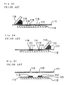
- the resist layer is omitted from illustration in Fig. 2A, 2B, and 2C.
- printing mask 111 is positioned on PCB 112 with through holes 116 defined therein being aligned with respective lands 115 on PCB 112. Then, a given amount of solder paste 113 is placed on printing mask 111 on PCB 112. As shown in Fig. 2B, solder paste 113 is turned and moved over printing mask 111 from one end to the other by squeegee 118.
- solder paste 113 As solder paste 113 is turned and moved over printing mask 111, it is pushed into through holes 116 by squeegee 118 and filled in through holes 116. As shown in Fig. 2C, when printing mask 111 is peeled off PCB 112, a given layer of solder paste 113 is printed on each land 115 on PCB 112. Now, the solder paste printing process is completed.
- solder fillets around the leads of the through-hole parts may be small or no solder fillets may be formed around the leads of the through-hole parts on the surface of the PCB opposite to the surface of the PCB that is printed with the solder paste. Therefore, the through-hole parts may not be well connected to the lands.
- solder bridge may be formed between the leads of the through-hole parts mounted on the PCB, and the solder paste flowing from between the leads may be turned into a number of balls (solder balls).
- Another object of the present invention is to provide a surface-mounted structural assembly in which electronic parts are reliably joined to lands on a PCB by a solder paste without causing the applied solder paste to extend between the lands, and a method of manufacturing such a surface-mounted structural assembly.
- a printing mask has a plurality of through holes for printing a solder paste on lands on a printed circuit board and at least one protrusion, at least one of the through holes being defined in the protrusion.
- the protrusion increases the depth of the through hole defined therein, a layer of solder paste filled in the through hole has an increased thickness. Therefore, the amount of the applied solder paste printed on the lands is increased without increasing the opening area of the through hole. The amount of the applied solder paste printed on any desired land on the printed circuit board can thus be increased reliably without producing a solder bridge or solder balls.
- the increased amount of the applied solder paste increases solder wettability with respect to through holes and leads in particular, allowing leads passing through the through holes to be joined reliably.
- the printing mask is used to print a solder paste on a printed circuit board which has a first land for placing a lead of an electronic part thereon and a second land including a through hole for passing a lead of the electronic part therethrough. Therefore, only the second land including the through hole for passing the lead of the electronic part therethrough should preferably be formed on the protrusion. As a result, since the depth of the through hole corresponding to the second land is greater than the depth of the through hole corresponding to the first land, the amount of the applied solder paste printed on the second land is greater than the amount of the applied solder paste printed on the first land.
- the solder paste preferably comprises an Sn - Zn alloy which is relatively poor in wettability.
- a method of printing a solder paste prints a solder plate on lands on a printed circuit using the above printing mask.
- a surface-mounted structural assembly comprising an electronic part mounted, by soldering, on a printed circuit board having a first land for placing a lead of an electronic part thereon and a second land including a through hole for passing a lead of the electronic part therethrough. Since a layer of solder paste printed on the second land is thicker than a layer of solder paste printed on the first land, the electronic part can reliably be joined to the second land.
- a method of manufacturing a surface-mounted structural assembly having an electronic part mounted on a printed circuit board by soldering comprising the steps of printing a solder paste on a printed circuit board using the printing mask according to the present invention, placing an electronic part on the printed circuit board, and joining the electronic part to the printed circuit board with the solder paste.
- the method makes it possible to manufacture a surface-mounted structural assembly comprising an electronic part-mounted, by soldering, on a printed circuit board having a first land for placing a lead of an electronic part thereon and a second land including a through hole for passing a lead of the electronic part therethrough.
- a layer of solder paste printed on the second land is thicker than a layer of solder paste printed on the first land. Therefore, the electronic part can reliably be joined to the second land.
- PCB 2 (see Figs. 5A, 5B, 5C and 6) which will be printed with a solder paste using printing mask 1 according to an embodiment of the present invention as shown in Figs. 3 and 4 has a plurality of first lands 5 for mounting surface-mount electronic parts and a plurality of second lands 6 for mounting through-hole parts whose leads are inserted in through holes in the PCB, first and second lands 5, 6 being located in predetermined positions. Second lands 6 extend between one surface of PCB 2 and the other surface of PCB 2, with through holes 7 defined respectively therein.
- printing mask 1 comprises a thin sheet of metal such as stainless steel or the like.
- Printing mask 1 has a plurality of first through holes 11 defined therein which correspond to first lands 5 on PCB 2 and a plurality of second through holes 12 defined therein which correspond to second lands 6 on PCB 2.
- First through holes 11 have a shape and an area which are substantially equal to the shape and area of first lands 5, and second through holes 12 have a shape which is substantially equal to the shape of second lands 6, and an area which is slightly larger than the area of second lands 6, about 0.1 mm through 0.2 mm greater than the outer circumferential edge of second lands 6.
- Printing mask 1 has annular protrusions 13, 14 integral with masking regions around second through holes 12. Annular protrusions 13, 14 are made thicker than other masking regions of printing mask 1 by a plating process or the like.
- printing mask 1 has a thickness t 1 of about 0.15 mm, and annular protrusions 13, 14 have a thickness t 2 ranging from 0.18 mm to 0.2 mm.
- Annular protrusions 13, 14 have an inside diameter ⁇ 1 of about 1.5 mm and an outside diameter ⁇ 2 of about 2.0 mm.
- Through holes defined in PCB 2 have a diameter ⁇ 3 of about 0.8 mm, and second lands 6 have an outside diameter of about 1.2 mm which is slightly smaller than the inside diameter ⁇ 1 of annular protrusions 13, 14.
- printing mask 1 has a thickness near second through holes 12 which is greater than the thickness of printing mask 1 near first through holes 11 in the other mask regions.
- Solder paste 3 comprises, for example, an Sn - Zn alloy such as Sn - 8Zn - 3Bi.
- PCB 2 has an interconnection pattern of copper foil covered with an insulating resist layer.
- First and second lands 5, 6 are provided on the PCB by removing the resist layer from portions of the interconnection pattern.
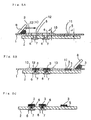
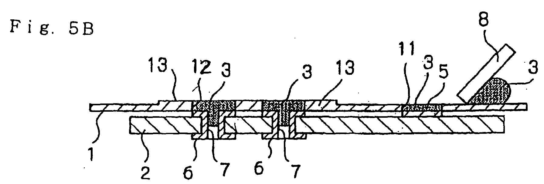
- the resist layer is omitted from illustration in Fig. 5A, 5B, and 5C.
- printing mask 1 is positioned on PCB 2 with first and second through holes 11, 12 being aligned with respective first and second lands 5, 6 on PCB 2. Then, a given amount of solder paste 3 is placed on printing mask 1 on PCB 2. As shown in Fig. 5B, solder paste 3 is turned and moved over printing mask 1 from one end to the other by squeegee 8.
- solder paste 3 As solder paste 3 is turned and moved over printing mask 1, it is pushed into first and second through holes 11, 12 by squeegee 8 and filled in first and second through holes 11, 12. Since second through holes 12 are deeper than first through holes 11, the solder paste 3 applied in a quantity depending on the depth of second through holes 12 is placed on second lands 6 on PCB2 and filled in through holes 7 in PCB 2.
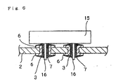
- leads 16 of a through-hole part 15 shown in Fig. 6 are inserted into through holes 7 filled with solder paste 3 from one side of PCB 2, leads 16 push filled solder paste 3 out of through holes 7 onto second lands 6 on the other side of PCB 2, thus placing a sufficient amount of solder paste 3 on second lands 6. Since the increased amount of solder paste 3 is supplied to second lands 6, its wettability with respect to leads 16 and through holes 7 is increased. Therefore, when through-hole part 15 placed on PCB 2 is joined by reflow soldering, through-hole part 15 is connected to second lands 6 with sufficient bonding strength.
- Printing mask 1 is capable of allowing solder paste 3 to be applied in an increased quantity to second lands 6 and through holes 7 without causing the problem of reduced distances between printed layers of solder paste 3 on adjacent second lands 6, which would otherwise result from an increase in the opening area of second through holes 12.
- through-hole part 15 joined to second lands 6 is well mounted on PCB by solder paste 3 without causing solder paste 3 to extend, as a solder bridge, between leads 16 on adjacent second lands 6 on the surface of PCB 2 where through-hole part 15 is mounted, i.e., where leads 16 are inserted, and also without causing solder paste 3 to flow from second lands 6 and to be turned into solder balls.
- Printing mask 1 and the printing process described above are applied to the printing of solder paste 3 to mount through-hole part 15 on one surface of PCB 2 after various surface-mount electronic parts have been mounted on the other surface of PCB 2.
- printing mask 1 and the printing process may be applied, if necessary, to the printing of the solder paste to mount other electronic parts than through-hole parts.
Landscapes
- Engineering & Computer Science (AREA)
- Manufacturing & Machinery (AREA)
- Microelectronics & Electronic Packaging (AREA)
- Electric Connection Of Electric Components To Printed Circuits (AREA)
- Screen Printers (AREA)
Abstract
Description
Claims (10)
- A printing mask having a plurality of through holes for printing a solder paste on lands on a printed circuit board and at least one protrusion, at least one of said through holes being defined in said protrusion.
- A printing mask according to claim 1, wherein only one of said through holes which corresponds to a land including a through hole for passage of a lead of an electronic part is defined in said protrusion.
- A printing mask according to claim 1 or 2, wherein each of said through holes has an opening area substantially equal to the area of said lands.
- A printing mask according to claim 1 or 2, wherein each of said through holes has an opening area slightly larger than the area of said lands.
- A printing mask according to claim 1, 2, 3 or 4, wherein said solder paste comprises an Sn - Zn alloy.
- A method of printing a solder paste, comprising the steps of:positioning a printing mask having a plurality of through holes for printing a solder paste on lands on a printed circuit board and at least one protrusion, with at least one of said through holes being defined in said protrusion, on said printed circuit board; andplacing and printing a solder plate on said printing mask to cover first and second lands of said lands, such that a layer of solder paste printed on said second land is thicker than a layer of solder paste printed on said first land.
- A surface-mounted structural assembly comprising:a printed circuit board having a first land for placing a lead of an electronic part thereon and a second land including a through hole for passing a lead of the electronic part therethrough;an electronic part mounted on said printed circuit board; anda solder paste printed on said first land and said second land;said electronic part being joined to said printed circuit board by said solder paste such that a layer of solder paste printed on said second land is thicker than a layer of solder paste printed on said first land.
- A surface-mounted structural assembly according to claim 7, wherein said solder paste comprises an Sn - Zn alloy.
- A method of manufacturing a surface-mounted structural assembly having an electronic part mounted on a printed circuit board by soldering, comprising the steps of:printing a solder paste on a printed circuit board using a printing mask having a plurality of through holes for printing a solder paste on lands on a printed circuit board and at least one protrusion, at least one of said through holes being defined in said protrusion;placing an electronic part on said printed circuit board; andjoining said electronic part to said printed circuit board with said solder paste.
- A method according to claim 9, wherein said solder paste comprises an Sn - Zn alloy.
Applications Claiming Priority (2)
| Application Number | Priority Date | Filing Date | Title |
|---|---|---|---|
| JP2001166909 | 2001-06-01 | ||
| JP2001166909A JP3846554B2 (en) | 2001-06-01 | 2001-06-01 | Mask for printing, printing method, mounting structure, and manufacturing method of the mounting structure |
Publications (2)
| Publication Number | Publication Date |
|---|---|
| EP1263272A2 true EP1263272A2 (en) | 2002-12-04 |
| EP1263272A3 EP1263272A3 (en) | 2004-06-16 |
Family
ID=19009380
Family Applications (1)
| Application Number | Title | Priority Date | Filing Date |
|---|---|---|---|
| EP02011643A Withdrawn EP1263272A3 (en) | 2001-06-01 | 2002-05-29 | Printing mask having protrusions with through holes for printing solder paste on lands on printed circuit board |
Country Status (6)
| Country | Link |
|---|---|
| US (1) | US6857361B2 (en) |
| EP (1) | EP1263272A3 (en) |
| JP (1) | JP3846554B2 (en) |
| KR (1) | KR100530965B1 (en) |
| CN (1) | CN1241461C (en) |
| TW (1) | TW552483B (en) |
Cited By (2)
| Publication number | Priority date | Publication date | Assignee | Title |
|---|---|---|---|---|
| WO2008155040A1 (en) * | 2007-06-20 | 2008-12-24 | Phoenix Contact Gmbh & Co. Kg | Restraining a connecting material |
| CN113942293A (en) * | 2021-10-14 | 2022-01-18 | 浪潮商用机器有限公司 | A through-hole solder paste printing device |
Families Citing this family (28)
| Publication number | Priority date | Publication date | Assignee | Title |
|---|---|---|---|---|
| US6395995B1 (en) * | 2000-03-15 | 2002-05-28 | Intel Corporation | Apparatus for coupling integrated circuit packages to bonding pads having vias |
| JP2004228276A (en) * | 2003-01-22 | 2004-08-12 | D D K Ltd | Method of connecting connector to substrate |
| JP2005026457A (en) * | 2003-07-02 | 2005-01-27 | Toshiba Corp | Electronic component mounting method, board manufacturing apparatus, and circuit board |
| US7331503B2 (en) * | 2004-10-29 | 2008-02-19 | Intel Corporation | Solder printing process to reduce void formation in a microvia |
| JP4720608B2 (en) * | 2006-05-10 | 2011-07-13 | パナソニック株式会社 | Component mounting apparatus and component mounting method |
| CN101453062B (en) * | 2007-12-03 | 2011-05-25 | 台达电子工业股份有限公司 | Surface mount connector, circuit board module and circuit board combination |
| JP2009224678A (en) * | 2008-03-18 | 2009-10-01 | Mitsubishi Electric Corp | Metal mask and printed wiring board |
| JP2010214680A (en) * | 2009-03-16 | 2010-09-30 | Panasonic Corp | Screen printing machine and method for cleaning screen printing machine |
| JP5240069B2 (en) * | 2009-05-25 | 2013-07-17 | パナソニック株式会社 | Screen printing mask cleaning apparatus, screen printing machine, and screen printing mask cleaning method |
| DE102009024873A1 (en) * | 2009-06-09 | 2010-12-16 | Nb Technologies Gmbh | Screen printing form has layer as screen printing stencil carrier, where layer is provided with recesses that are formed such that they reach from upper side to lower side of layer |
| KR20110037642A (en) * | 2009-10-07 | 2011-04-13 | 삼성전기주식회사 | Mask for solder printing and printed circuit board manufacturing method using the same |
| FR2954606B1 (en) * | 2009-12-23 | 2019-05-10 | Valeo Systemes Thermiques | CONNECTOR FOR ELECTRIC CIRCUIT BOARD, ELECTRICAL CIRCUIT BOARD AND CORRESPONDING ELECTRICAL HEATING DEVICE |
| TWI426842B (en) * | 2011-07-22 | 2014-02-11 | Taidoc Technology Corp | Electronic device and surface mounting method |
| TWI426841B (en) * | 2011-07-22 | 2014-02-11 | Taidoc Technology Corp | Electronic device and surface mounting method |
| US20130025922A1 (en) * | 2011-07-29 | 2013-01-31 | Weibezahn Karl S | Bonding entities to conjoined strips of conductive material |
| US9426901B2 (en) * | 2011-10-12 | 2016-08-23 | General Electric Company | Patterning method for component boards |
| CN103386524A (en) * | 2012-05-08 | 2013-11-13 | 光宝电子(广州)有限公司 | Welding method |
| US20140055961A1 (en) * | 2012-08-23 | 2014-02-27 | Shayan Malek | Printed Circuit Boards with Recesses |
| SE537793C2 (en) * | 2012-08-29 | 2015-10-20 | Jan Berglund Med Inco Innovation F | Power conductor mounted on a circuit board |
| CN103716987B (en) * | 2012-10-09 | 2017-04-26 | 讯忆科技股份有限公司 | Blind hole conduction structure of printed circuit board and manufacturing method thereof |
| TWI499893B (en) * | 2013-04-01 | 2015-09-11 | Innolux Corp | Display module and display device containing the same |
| CN107135612A (en) * | 2017-05-31 | 2017-09-05 | 郑州云海信息技术有限公司 | The positioning auxiliary device and localization method of a kind of pcb board |
| KR101890197B1 (en) * | 2018-03-26 | 2018-08-21 | 주식회사 제이앤티씨 | Processing method of ear socket connector for smartphone |
| CN108337821B (en) * | 2018-04-20 | 2019-08-16 | 汉通(沧州)电子有限公司 | A kind of welding method of circuit board |
| US11033990B2 (en) * | 2018-11-29 | 2021-06-15 | Raytheon Company | Low cost approach for depositing solder and adhesives in a pattern for forming electronic assemblies |
| CN111627824A (en) * | 2020-06-09 | 2020-09-04 | 山东新恒汇电子科技有限公司 | Flip-mount packaging carrier tape for realizing roll-to-roll production of CSP chips and manufacturing method thereof |
| CN115226304B (en) * | 2021-04-20 | 2025-03-21 | 庆鼎精密电子(淮安)有限公司 | Circuit board and method for manufacturing the same |
| JP7648582B2 (en) * | 2022-11-15 | 2025-03-18 | カヤバ株式会社 | Manufacturing method of the circuit unit |
Family Cites Families (25)
| Publication number | Priority date | Publication date | Assignee | Title |
|---|---|---|---|---|
| JPS61144396A (en) * | 1984-12-19 | 1986-07-02 | Kiyoushiya:Kk | Screen plate-making |
| US4919970A (en) * | 1986-09-15 | 1990-04-24 | International Business Machines Corporation | Solder deposition control |
| US4872261A (en) * | 1987-12-11 | 1989-10-10 | Digital Equipment Corporation | Method of and apparatus for surface mounting electronic components onto a printed wiring board |
| JPH02107487A (en) * | 1988-10-17 | 1990-04-19 | Mitsubishi Electric Corp | Metallic mask for printing use |
| JPH0491861A (en) * | 1990-08-06 | 1992-03-25 | Matsushita Electric Ind Co Ltd | Metallic mask for cream solder printing |
| JPH04336490A (en) * | 1991-05-13 | 1992-11-24 | Sharp Corp | Method for forming reflow solder |
| JPH05177965A (en) * | 1992-01-07 | 1993-07-20 | Matsushita Electric Ind Co Ltd | Metal mask structure for cream solder printing |
| JPH06252152A (en) * | 1993-02-22 | 1994-09-09 | Ibiden Co Ltd | Formation of solder bump on ceramic wiring board |
| JP3327417B2 (en) * | 1993-04-22 | 2002-09-24 | 日本アビオニクス株式会社 | Metal mask |
| US5390080A (en) * | 1993-05-03 | 1995-02-14 | Motorola | Tin-zinc solder connection to a printed circuit board of the like |
| JPH07101033A (en) * | 1993-09-30 | 1995-04-18 | Canon Inc | Screen mask forming method |
| JPH07263857A (en) * | 1994-03-22 | 1995-10-13 | Melco:Kk | How to mount electronic components on a printed wiring board |
| JP3238029B2 (en) | 1995-01-17 | 2001-12-10 | リコーマイクロエレクトロニクス株式会社 | Plastic mask for paste printing and paste printing method using the same |
| JPH08195548A (en) * | 1995-01-17 | 1996-07-30 | Matsushita Electric Ind Co Ltd | Electronic component mounting method |
| JPH09130028A (en) * | 1995-10-30 | 1997-05-16 | Hitachi Ltd | Liquid crystal display device equipped with a solder printing mask and a printed circuit board manufactured using this mask |
| GB2307446A (en) | 1995-11-25 | 1997-05-28 | Ibm | Solder paste deposition |
| JPH1044369A (en) * | 1996-08-01 | 1998-02-17 | Fujitsu Ten Ltd | Solder printer |
| KR19980059239A (en) * | 1996-12-31 | 1998-10-07 | 김광호 | Chip on board package and manufacturing method thereof |
| JPH10224024A (en) * | 1997-02-03 | 1998-08-21 | Fujitsu Ten Ltd | Parts mounting method |
| JPH1174638A (en) * | 1997-08-29 | 1999-03-16 | Toshiba Corp | Cream solder printing method and metal mask |
| JPH11177224A (en) * | 1997-12-12 | 1999-07-02 | Matsushita Electric Ind Co Ltd | Metal mask and printed wiring board |
| US6316736B1 (en) * | 1998-06-08 | 2001-11-13 | Visteon Global Technologies, Inc. | Anti-bridging solder ball collection zones |
| US6273327B1 (en) * | 1999-06-16 | 2001-08-14 | Trw Inc. | Apparatus and method for depositing solder material onto a circuit board |
| JP4143280B2 (en) * | 2001-06-01 | 2008-09-03 | 日本電気株式会社 | Mounting structure, method for manufacturing mounting structure, mask for printing, and printing method |
| JP4181759B2 (en) * | 2001-06-01 | 2008-11-19 | 日本電気株式会社 | Electronic component mounting method and mounting structure manufacturing method |
-
2001
- 2001-06-01 JP JP2001166909A patent/JP3846554B2/en not_active Expired - Fee Related
-
2002
- 2002-05-23 TW TW091110905A patent/TW552483B/en not_active IP Right Cessation
- 2002-05-29 EP EP02011643A patent/EP1263272A3/en not_active Withdrawn
- 2002-05-30 CN CNB021221197A patent/CN1241461C/en not_active Expired - Fee Related
- 2002-05-31 US US10/159,474 patent/US6857361B2/en not_active Expired - Fee Related
- 2002-06-01 KR KR10-2002-0030866A patent/KR100530965B1/en not_active Expired - Fee Related
Cited By (5)
| Publication number | Priority date | Publication date | Assignee | Title |
|---|---|---|---|---|
| WO2008155040A1 (en) * | 2007-06-20 | 2008-12-24 | Phoenix Contact Gmbh & Co. Kg | Restraining a connecting material |
| CN101690432B (en) * | 2007-06-20 | 2012-02-01 | 菲尼克斯电气公司 | Forced guidance a connecting material |
| US8276272B2 (en) | 2007-06-20 | 2012-10-02 | Phoenix Contact Gmbh & Co. Kg | Method for applying a connection material |
| CN113942293A (en) * | 2021-10-14 | 2022-01-18 | 浪潮商用机器有限公司 | A through-hole solder paste printing device |
| CN113942293B (en) * | 2021-10-14 | 2023-08-08 | 浪潮商用机器有限公司 | A through-hole solder paste printing device |
Also Published As
| Publication number | Publication date |
|---|---|
| TW552483B (en) | 2003-09-11 |
| JP2002361832A (en) | 2002-12-18 |
| KR20020092254A (en) | 2002-12-11 |
| US6857361B2 (en) | 2005-02-22 |
| CN1241461C (en) | 2006-02-08 |
| EP1263272A3 (en) | 2004-06-16 |
| CN1392762A (en) | 2003-01-22 |
| US20020185020A1 (en) | 2002-12-12 |
| KR100530965B1 (en) | 2005-11-28 |
| JP3846554B2 (en) | 2006-11-15 |
Similar Documents
| Publication | Publication Date | Title |
|---|---|---|
| US6857361B2 (en) | Method and apparatus for printing solder paste of different thickness on lands on printed circuit board | |
| US6849805B2 (en) | Printed wiring board and electronic apparatus | |
| KR100483394B1 (en) | A method of packaging electronic components with high reliability | |
| CN100423621C (en) | Land portion of printed wiring board, method for manufacturing printed wiring board, and method for mounting component on printed wiring board | |
| EP1855517A1 (en) | Soldering structure of through hole | |
| US20020179328A1 (en) | Method of mounting electronic parts with Sn-Zn solder free of Pb without reduction in bonding strength | |
| JP4143280B2 (en) | Mounting structure, method for manufacturing mounting structure, mask for printing, and printing method | |
| KR100488222B1 (en) | A method of fabricating packaged construction, packaged construction, and metal mask | |
| JP2002190664A (en) | Printed wiring board and semiconductor device using the same | |
| EP1135011A2 (en) | Printed-wiring board | |
| KR19990026398A (en) | Parts mounting method of printed circuit board | |
| KR810000847B1 (en) | Manufacturing method for printed circuit | |
| JP3189209B2 (en) | Surface mounting method for electronic components | |
| JP2004055662A (en) | Soldering method and its printed wiring board | |
| JP2005311394A (en) | Mounting structure and manufacturing method therefor, mask for printing, and printing method | |
| JP2005354096A (en) | Method for mounting electronic component, and method for manufacturing mounting structure | |
| JPH0736473U (en) | Printed wiring board | |
| JP2002158430A (en) | Circuit board and soldering method | |
| KR19990026830A (en) | Printed Circuit Board Soldering Method | |
| JP2001217533A (en) | How to solder components | |
| JPH07249858A (en) | Surface mounting method of printed wiring board |
Legal Events
| Date | Code | Title | Description |
|---|---|---|---|
| PUAI | Public reference made under article 153(3) epc to a published international application that has entered the european phase |
Free format text: ORIGINAL CODE: 0009012 |
|
| AK | Designated contracting states |
Kind code of ref document: A2 Designated state(s): AT BE CH CY DE DK ES FI FR GB GR IE IT LI LU MC NL PT SE TR |
|
| AX | Request for extension of the european patent |
Free format text: AL;LT;LV;MK;RO;SI |
|
| PUAL | Search report despatched |
Free format text: ORIGINAL CODE: 0009013 |
|
| AK | Designated contracting states |
Kind code of ref document: A3 Designated state(s): AT BE CH CY DE DK ES FI FR GB GR IE IT LI LU MC NL PT SE TR |
|
| AX | Request for extension of the european patent |
Extension state: AL LT LV MK RO SI |
|
| 17P | Request for examination filed |
Effective date: 20040504 |
|
| AKX | Designation fees paid |
Designated state(s): DE FR GB |
|
| 17Q | First examination report despatched |
Effective date: 20070503 |
|
| STAA | Information on the status of an ep patent application or granted ep patent |
Free format text: STATUS: THE APPLICATION IS DEEMED TO BE WITHDRAWN |
|
| 18D | Application deemed to be withdrawn |
Effective date: 20070914 |