EP1263162B1 - Device and method for the digital demodulation of a signal received by selecting a filter and digital communication receiver comprising the same - Google Patents
Device and method for the digital demodulation of a signal received by selecting a filter and digital communication receiver comprising the same Download PDFInfo
- Publication number
- EP1263162B1 EP1263162B1 EP02291299A EP02291299A EP1263162B1 EP 1263162 B1 EP1263162 B1 EP 1263162B1 EP 02291299 A EP02291299 A EP 02291299A EP 02291299 A EP02291299 A EP 02291299A EP 1263162 B1 EP1263162 B1 EP 1263162B1
- Authority
- EP
- European Patent Office
- Prior art keywords
- elementary
- filter
- block
- samples
- digital
- Prior art date
- Legal status (The legal status is an assumption and is not a legal conclusion. Google has not performed a legal analysis and makes no representation as to the accuracy of the status listed.)
- Expired - Lifetime
Links
Images
Classifications
-
- H—ELECTRICITY
- H04—ELECTRIC COMMUNICATION TECHNIQUE
- H04L—TRANSMISSION OF DIGITAL INFORMATION, e.g. TELEGRAPHIC COMMUNICATION
- H04L7/00—Arrangements for synchronising receiver with transmitter
- H04L7/0016—Arrangements for synchronising receiver with transmitter correction of synchronization errors
- H04L7/002—Arrangements for synchronising receiver with transmitter correction of synchronization errors correction by interpolation
- H04L7/0029—Arrangements for synchronising receiver with transmitter correction of synchronization errors correction by interpolation interpolation of received data signal
Definitions
- the clocks of the two entities are only rarely exactly synchronized in terms of frequency and phase, so that a time shift exists between the time bases supplied by the two clocks.
- US-A-6 141 378 discloses a fractionally-spaced adaptively equalized self recovering digital receiver for amplitude-phase modulated signals.
- devices for the digital demodulation of a signal sometimes comprise decimating means, as set forth above.
- decimation requires recourse to means for determining the samples to be selected during decimation.
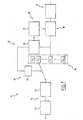
- the device 10 illustrated in Figure 1 is suitable for the digital demodulation of a modulated communication signal. It is intended to be implemented in a digital communication receiver, such as a mobile telephone or a base station of a wireless telecommunication network.
- the digitizing stage 24 is suitable for digitizing, with an oversampling factor denoted P, the modulated signal.
- the oversampling factor is equal to the number P of samples per symbol. The latter is advantageously as small as possible. It is however, greater than or equal to 2. It is advantageously less than or equal to 4 in the device according to the invention.
- the in-phase and quadrature parts are processed either independently of one another according to similar algorithms, or jointly.
- This chopping into blocks is performed on each of the in-phase I and quadrature Q parts of the signal.
- the subsequent processes performed in the means 13 for correcting the sampling instant are performed block by block so as to reduce the time for loading and for booting the functions introduced by the process for calling functions.
- the phase corrections in the corrector 22 are established block by block, the phase errors being assumed stationary or negligible over a block.
- the blocks obtained at the output of the chopping stage 26 are then processed by the complex polyphase filter 14.
- This polyphase filter 14 comprises N elementary complex filters or branches. Each elementary filter is denoted H i with i ⁇ [0,...,N-1].
- the number N of polyphase filters is for example equal to 8, 16, 32, 64, 128, 256 or more. It is not compulsory for this number to be a power of 2.
- the number of filters is preferably large and is advantageously greater than 256.
- the oversampling factor P is chosen small while the number N of elementary filters is chosen large.
- the ratio P/N is less than 1.
- the polyphase filter 14 is implemented by a processor associated with means for storing a functional definition of each elementary filter H i .
- each filter is constituted by a table of coefficients.
- N tables of coefficients are stored.
- Each table of coefficients represents the digitization, previously performed, of the impulse response of the relevant elementary filter H i , each for a given phase or shift as explained hereinbelow.
- the in-phase I and quadrature Q parts of each block are processed by one and the same elementary filter H i of the polyphase filter.
- the complex polyphase filter is built from two identical polyphase filters, one for the in-phase part, the other for the quadrature part.
- Each elementary filter of the polyphase filter is constituted by the digitization of the reception filter for a sampling period denoted Te.
- the phase variation of the N elementary filters spreads from -Te/2 to (Te/2 - Te/N) so as to cover a complete sampling period Te.
- Each elementary filter H i has a phase shifted by 1/Nth of a sampling period Te with respect to the previous elementary filter H i-1 .
- N the smaller is the phasewise discretization spacing, thus leading to the possibility of correcting the sampling instant accurately.
- Each elementary filter is a particular version of one and the same reference reception filter, and in this regard complies with the frequency-selective nature thereof.
- Each elementary filter can advantageously ensure the suppression of inter-symbol interference.
- a filter of "Root Raised Cosine" type can advantageously serve as a basis for the definition of each of the elementary filters associated with distinct phases.
- the reference reception filter serving as basis, to within the phase variation, for the elementary filters is suitable for limiting the noise, and is known per se.
- These means 16 comprise a stage 28 for computing an error signal in respect of a relevant block.
- the error signal produced by the stage 28 is individual to the mode of modulation used for the transmission of the data.
- the example which follows is suitable for PSK type modulations.
- the error signal is formed of the set of standard deviations ⁇ computed over the moduli of all the symbols belonging to a block, for each of the P sampling instants for one and the same symbol.
- the error signal supplied by the stage 28 is used by a selection stage 30 making it possible to select the elementary filter H i of the polyphase filter by implementing the tracking algorithm.
- the same error signal is furthermore used by a stage 31 for evaluating the error signal of the means 20 for determining the shift of the decimation index controlling the means 18.
- the stage 31 of the means 20 is suitable for selecting the minimum standard deviation ⁇ k appearing in the error signal.
- the selecting of the minimum standard deviation ⁇ k leads to the reducing of the phase error and constitutes the error criterion making it possible to control the decimating stage 18 on the basis of the index k ⁇ corresponding to the minimum standard deviation.
- the stage 31 determines, from the error signal supplied by the error computation stage 28, the shift k ⁇ as being the index of the sampling instant corresponding to the minimum of the computed standard deviations.
- the stage 31 is suitable for controlling a decimation leading to the largest aperture of the eye diagram.
- the decimating stage 18 is suitable for extracting L samples per block from the samples received at the output of the polyphase filter 14, while retaining only one sample out of P samples from the k ⁇ th sample. Hence, only one sample per symbol remains.
- the decimated data are then addressed to the phase corrector 22.
- the phase correction can be performed using two types of algorithms: either using an algorithm employing the a priori knowledge of the data to be transmitted, or using an algorithm not employing same.
- This phase correction is applied to the decimated samples so as to compensate for the phase rotations introduced by:
- a block-by-block update thus makes it possible to achieve carrier synchronization.
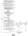
- the complex polyphase filter 14, the stages for computing the error signal 28, the selection stage 30, the evaluation stage 31 and the decimation stage 18 are implemented by one or more computers executing a suitable program, the main algorithm of which is illustrated in Figure 2 .
- the manner of operation of the selection stage 30 is illustrated in particular in this algorithm.
- the device receives a modulated signal.
- step 100 the digitizing stage 24 ensures demodulation of the signal with an oversampling by a factor P, and puts the digitized signal into baseband.
- the digitized baseband signal is then processed block after block by implementing a loop.
- step 102 the digitized signal is chopped into blocks of S samples, the successive blocks being denoted B 1 .
- step 104 the relevant block B 1 is processed by an elementary digital filter H i of the polyphase filter 14.
- the index i of the elementary filter H i implemented is determined by the selection stage 30. This selection algorithm is described later.
- the elementary filter implemented is selected arbitrarily.
- the computer For the processing of the samples by the selected elementary filter, the computer implements the table of coefficients individual to the elementary filter H i , this elementary table being selected in memory by a pointer defined by the selection means 30.
- the elementary filters H i are ordered according to the order of the indices in ascending or descending order of phase.
- step 106 the stage 28 performs the computation of the error signal. Accordingly, a loop is implemented in which is computed, in step 108, the set of standard deviations associated with the block B 1 for each of the oversampling indices lying between 0 and P - 1. These standard deviations forming the error signal are denoted ⁇ 1,j .
- step 114 the decimation stage 18 ensures the extraction of the L samples from the samples received, retaining only one sample out of P from the k ⁇ th sample determined in step 112.
- step 116 the phase corrector 22 processes the filtered and decimated block B 1 .
- Steps 102 et seq. are again implemented for the next block B 1+1 .
- the selection stage 30 implements the tracking algorithm corresponding to the routine 118 of the algorithm of Figure 2 .
- the aim of this algorithm is to determine the elementary filter H i of the polyphase filter most suitable for the reception process in respect of the next block B 1+1 .
- This elementary filter H i adopted is the one which makes it possible to minimize the standard deviation ⁇ of the modulus of the decimated data.
- the tracking algorithm is used so as to avoid computing the standard deviation ⁇ of the modulus of all the elementary filters H i of the polyphase filter 14.
- This algorithm requires the storage from one block to another:
- the direction of tracking is given by a variable denoted s which can take the values +m and -m, with m ⁇ N and m ⁇ N.
- s denoted s which can take the values +m and -m, with m ⁇ N and m ⁇ N.
- m 1.
- the value +m corresponds to an incrementation of the indices among the elementary filters of m ranks and the value -m corresponding to a traversal of m ranks in the direction of descending indices among the elementary filters.
- step 120 a test is performed to compare the current standard deviation ⁇ 1,k associated with the elementary filter H i used for block B 1 with the decimation standard deviation ⁇ 1-1,k associated with the elementary filter H j used for the previous block B 1-1 . If the current decimation standard deviation ⁇ 1,k is less than the previous decimation standard deviation ⁇ 1-1,k , the direction of tracking is kept unchanged in step 122.
- step 124 the index of the elementary filter H i which has to be used for the next block B 1+1 is computed by incrementation modulo N of the index of the filter previously used by the value s.
- the selected elementary filter is H i+s .
- the computation modulo N of the next index makes it possible to keep the index i in the interval [0, N-1].
- the elementary filter index is either incremented by the value m or decremented by the value m according to the direction of tracking.
- the decimation of the block will itself be done with a decimation index modified by P-1 units, since the sample representative of the symbol changes.
- the tracking algorithm comprises three phases:
- the polyphase filter of the demodulating device being implemented by a computer using for each elementary filter a previously stored functional definition of the filter makes it possible to use a polyphase filter having a very large number of elementary filters.
- the footprint on the circuit is limited to the footprint of the processor and of the associated memories. The latter are moreover very often integrated into the processor.
- a great many tables of coefficients representative of the impulse response of an elementary filter may be stored in a memory having a small footprint.
- the initial signal is virtually oversampled by a factor N x P. Stated otherwise, it is possible to obtain the quality of a signal oversampled by a factor N x P, while making the processor carry out only the computations for the case of a signal oversampled by a factor P.
- the oversampling coefficient P being small, the computation time for the implementation of an elementary filter is much reduced, thereby making it possible to demodulate the data with a high real-time throughput.
- each of the elementary filters of the polyphase filter corresponds to a noise limitation filter.
- the polyphase filter increases the complexity of the device, the latter will not be compounded with the other elements normally constituting the demodulating device and will merely be integrated into the noise limitation filter.
- the tracking method used for selecting the elementary filter of the polyphase filter for each block converges rapidly towards a satisfactory filtering solution.
- This method makes it possible to compute just one error signal for each block and to compare just the standard deviations corresponding to the error signals of the previous block.
- the algorithm requires only reduced computational power. It is also conceivable to make the procedure more robust by averaging the error signal over several blocks.
- the computer has only few computations to perform, thus increasing the speed of implementation of the demodulation method.
- the value of the spacing m used in the tracking algorithm can be modified during the implementation of the algorithm.
- the value m of the spacing may be chosen large, then may be reduced automatically during the implementation of the algorithm, eventually being equal to the value 1, when the algorithm is in its steady state regime.
- the steady state regime can be detected by the presence of a succession of reversals of the direction of tracking.
- the demodulating device is implemented by a computer operating according to a suitable algorithm.
- This solution is advantageous for the reasons already set forth.
- the device can be implemented by hardware rather than software means, ensuring digital and/or analogue processing of the signal on the basis of circuits whose wiring and structure are suitable for performing the various functions required.
Landscapes
- Engineering & Computer Science (AREA)
- Computer Networks & Wireless Communication (AREA)
- Signal Processing (AREA)
- Digital Transmission Methods That Use Modulated Carrier Waves (AREA)
- Circuits Of Receivers In General (AREA)
- Communication Control (AREA)
- Radio Transmission System (AREA)
- Reduction Or Emphasis Of Bandwidth Of Signals (AREA)
Applications Claiming Priority (2)
| Application Number | Priority Date | Filing Date | Title |
|---|---|---|---|
| FR0107095 | 2001-05-30 | ||
| FR0107095A FR2825550B1 (fr) | 2001-05-30 | 2001-05-30 | Dispositif et procede de demodulation numerique d'un signal recu par selection d'un filtre et recepteur de communication numerique le comportant |
Publications (3)
| Publication Number | Publication Date |
|---|---|
| EP1263162A1 EP1263162A1 (en) | 2002-12-04 |
| EP1263162A8 EP1263162A8 (en) | 2003-07-23 |
| EP1263162B1 true EP1263162B1 (en) | 2008-10-01 |
Family
ID=8863784
Family Applications (1)
| Application Number | Title | Priority Date | Filing Date |
|---|---|---|---|
| EP02291299A Expired - Lifetime EP1263162B1 (en) | 2001-05-30 | 2002-05-28 | Device and method for the digital demodulation of a signal received by selecting a filter and digital communication receiver comprising the same |
Country Status (6)
| Country | Link |
|---|---|
| US (1) | US7184498B2 (enExample) |
| EP (1) | EP1263162B1 (enExample) |
| JP (1) | JP3986890B2 (enExample) |
| AT (1) | ATE409994T1 (enExample) |
| DE (1) | DE60229085D1 (enExample) |
| FR (1) | FR2825550B1 (enExample) |
Families Citing this family (5)
| Publication number | Priority date | Publication date | Assignee | Title |
|---|---|---|---|---|
| GB0609601D0 (en) * | 2006-05-15 | 2006-06-21 | Ttp Communications Ltd | Timing errors |
| US7411531B2 (en) * | 2006-06-30 | 2008-08-12 | Agere Systems Inc. | Methods and apparatus for asynchronous sampling of a received signal at a downsampled rate |
| JP5311831B2 (ja) * | 2008-01-11 | 2013-10-09 | 富士通株式会社 | 通信装置、ノイズキャンセラ、ノイズ除去方法およびノイズ除去プログラム |
| US8653868B2 (en) * | 2012-06-28 | 2014-02-18 | Intel Corporation | Low power data recovery |
| JP6615139B2 (ja) * | 2017-03-10 | 2019-12-04 | 三菱電機株式会社 | アレーアンテナの制御装置、アンテナ装置および移動通信用無線通信装置 |
Family Cites Families (7)
| Publication number | Priority date | Publication date | Assignee | Title |
|---|---|---|---|---|
| US5323391A (en) * | 1992-10-26 | 1994-06-21 | Motorola, Inc. | Multi-channel digital transmitter and receiver |
| DE4315806B4 (de) * | 1993-05-12 | 2005-07-28 | Robert Bosch Gmbh | Verfahren zur entscheidungsrückgekoppelten Taktregelung |
| US5504785A (en) * | 1993-05-28 | 1996-04-02 | Tv/Com Technologies, Inc. | Digital receiver for variable symbol rate communications |
| KR0170301B1 (ko) * | 1995-10-30 | 1999-04-15 | 김광호 | 복합위상여파기와 이를 이용한 타이밍 오차 보상장치 및 그 방법 |
| US5970093A (en) * | 1996-01-23 | 1999-10-19 | Tiernan Communications, Inc. | Fractionally-spaced adaptively-equalized self-recovering digital receiver for amplitude-Phase modulated signals |
| FI102338B1 (fi) * | 1996-05-21 | 1998-11-13 | Nokia Mobile Phones Ltd | Vastaanottimen tahdistuminen joutotilassa |
| US6134268A (en) * | 1998-10-19 | 2000-10-17 | Motorola, Inc. | Apparatus for performing a non-integer sampling rate change in a multichannel polyphase filter |
-
2001
- 2001-05-30 FR FR0107095A patent/FR2825550B1/fr not_active Expired - Fee Related
-
2002
- 2002-05-23 JP JP2002148881A patent/JP3986890B2/ja not_active Expired - Fee Related
- 2002-05-28 EP EP02291299A patent/EP1263162B1/en not_active Expired - Lifetime
- 2002-05-28 DE DE60229085T patent/DE60229085D1/de not_active Expired - Lifetime
- 2002-05-28 AT AT02291299T patent/ATE409994T1/de not_active IP Right Cessation
- 2002-05-30 US US10/157,156 patent/US7184498B2/en not_active Expired - Fee Related
Also Published As
| Publication number | Publication date |
|---|---|
| EP1263162A8 (en) | 2003-07-23 |
| US7184498B2 (en) | 2007-02-27 |
| FR2825550A1 (fr) | 2002-12-06 |
| FR2825550B1 (fr) | 2003-09-05 |
| DE60229085D1 (de) | 2008-11-13 |
| JP3986890B2 (ja) | 2007-10-03 |
| ATE409994T1 (de) | 2008-10-15 |
| US20030021362A1 (en) | 2003-01-30 |
| JP2003032312A (ja) | 2003-01-31 |
| EP1263162A1 (en) | 2002-12-04 |
Similar Documents
| Publication | Publication Date | Title |
|---|---|---|
| EP1263181B1 (en) | Sampling correction for a digital demodulation system and method using polyphase filter selection | |
| CA2170344C (en) | Signal processing system | |
| EP0772330A2 (en) | Receiver and method for receiving OFDM signals | |
| US5872818A (en) | Apparatus for recovering full digital symbol timing | |
| JPS61198848A (ja) | デ−タ受信システム | |
| JPH1117761A (ja) | 受信装置及び送受信装置並びに通信方法 | |
| US5867532A (en) | Data reception apparatus, data transmission apparatus and method thereof | |
| JP3058870B1 (ja) | Afc回路 | |
| US5062123A (en) | Kalman predictor for providing a relatively noise free indication of the phase of a carrier laden with noise | |
| EP1263162B1 (en) | Device and method for the digital demodulation of a signal received by selecting a filter and digital communication receiver comprising the same | |
| US6438567B2 (en) | Method for selective filtering | |
| KR100504761B1 (ko) | 직교 진폭 변조를 위한 구성 성분의 타이밍 회복 시스템 | |
| US7127019B2 (en) | Methods and apparatus for implementing multi-tone receivers | |
| Watkins | Optimal Farrow coefficients for symbol timing recovery | |
| EP0583643A1 (en) | Wholly-digital demodulation system for QAM signalling in low capacity links | |
| EP0851640B1 (en) | Correction of DC and phase offsets in PSK receivers | |
| EP1045561A2 (en) | Frequency correction in multicarrier receivers | |
| WO2005088923A1 (en) | Fast fourier transformation (fft) with adaption of the sampling rate in digital radio mondiale (drm) receivers | |
| CA2281462A1 (en) | Time error compensation arrangement and multi-carrier modem comprising the arrangement | |
| US7280614B2 (en) | Synchronization and equalization device for a digital transmission system receiver | |
| US7333579B2 (en) | Robust symbol timing recovery circuit for telephone line modem | |
| US7609795B2 (en) | Interpolation module, interpolator and methods capable of recovering timing in a timing recovery apparatus | |
| EP1693954B1 (en) | Demodulation circuit for use in receiver using IF sampling scheme | |
| KR100433639B1 (ko) | 잔류측파대변조시타이밍회복을위한장치및방법 | |
| Fines et al. | Fully digital M-ary PSK and M-ary QAM demodulators for land mobile satellite communications |
Legal Events
| Date | Code | Title | Description |
|---|---|---|---|
| PUAI | Public reference made under article 153(3) epc to a published international application that has entered the european phase |
Free format text: ORIGINAL CODE: 0009012 |
|
| AK | Designated contracting states |
Kind code of ref document: A1 Designated state(s): AT BE CH CY DE DK ES FI FR GB GR IE IT LI LU MC NL PT SE TR |
|
| AX | Request for extension of the european patent |
Free format text: AL;LT;LV;MK;RO;SI |
|
| RAP1 | Party data changed (applicant data changed or rights of an application transferred) |
Owner name: MITSUBISHI ELECTRIC CORPORATION INFORMATION TECHNO Owner name: MITSUBISHI ELECTRIC INFORMATION TECHNOLOGY CENTRE |
|
| RAP1 | Party data changed (applicant data changed or rights of an application transferred) |
Owner name: MITSUBISHI DENKI KABUSHIKI KAISHA Owner name: MITSUBISHI ELECTRIC INFORMATION TECHNOLOGY CENTRE |
|
| AKX | Designation fees paid | ||
| 17P | Request for examination filed |
Effective date: 20030502 |
|
| RBV | Designated contracting states (corrected) |
Designated state(s): AT BE CH CY DE DK ES FI FR GB GR IE IT LI LU MC NL PT SE TR |
|
| REG | Reference to a national code |
Ref country code: DE Ref legal event code: 8566 |
|
| RAP1 | Party data changed (applicant data changed or rights of an application transferred) |
Owner name: MITSUBISHI ELECTRIC INFORMATION TECHNOLOGY CENTRE Owner name: MITSUBISHI DENKI KABUSHIKI KAISHA |
|
| RAP1 | Party data changed (applicant data changed or rights of an application transferred) |
Owner name: MITSUBISHI ELECTRIC INFORMATION TECHNOLOGY CENTRE Owner name: MITSUBISHI DENKI KABUSHIKI KAISHA |
|
| RAP1 | Party data changed (applicant data changed or rights of an application transferred) |
Owner name: MITSUBISHI ELECTRIC INFORMATION TECHNOLOGY CENTRE Owner name: MITSUBISHI DENKI KABUSHIKI KAISHA |
|
| 17Q | First examination report despatched |
Effective date: 20061004 |
|
| GRAP | Despatch of communication of intention to grant a patent |
Free format text: ORIGINAL CODE: EPIDOSNIGR1 |
|
| RTI1 | Title (correction) |
Free format text: DEVICE AND METHOD FOR THE DIGITAL DEMODULATION OF A SIGNAL RECEIVED BY SELECTING A FILTER AND DIGITAL COMMUNICATION RECEIVER COMPRISING THE SAME |
|
| GRAS | Grant fee paid |
Free format text: ORIGINAL CODE: EPIDOSNIGR3 |
|
| GRAA | (expected) grant |
Free format text: ORIGINAL CODE: 0009210 |
|
| AK | Designated contracting states |
Kind code of ref document: B1 Designated state(s): AT BE CH CY DE DK ES FI FR GB GR IE IT LI LU MC NL PT SE TR |
|
| REG | Reference to a national code |
Ref country code: GB Ref legal event code: FG4D |
|
| REG | Reference to a national code |
Ref country code: CH Ref legal event code: EP |
|
| REG | Reference to a national code |
Ref country code: IE Ref legal event code: FG4D |
|
| REF | Corresponds to: |
Ref document number: 60229085 Country of ref document: DE Date of ref document: 20081113 Kind code of ref document: P |
|
| NLV1 | Nl: lapsed or annulled due to failure to fulfill the requirements of art. 29p and 29m of the patents act | ||
| PG25 | Lapsed in a contracting state [announced via postgrant information from national office to epo] |
Ref country code: AT Free format text: LAPSE BECAUSE OF FAILURE TO SUBMIT A TRANSLATION OF THE DESCRIPTION OR TO PAY THE FEE WITHIN THE PRESCRIBED TIME-LIMIT Effective date: 20081001 Ref country code: ES Free format text: LAPSE BECAUSE OF FAILURE TO SUBMIT A TRANSLATION OF THE DESCRIPTION OR TO PAY THE FEE WITHIN THE PRESCRIBED TIME-LIMIT Effective date: 20090112 |
|
| PG25 | Lapsed in a contracting state [announced via postgrant information from national office to epo] |
Ref country code: PT Free format text: LAPSE BECAUSE OF FAILURE TO SUBMIT A TRANSLATION OF THE DESCRIPTION OR TO PAY THE FEE WITHIN THE PRESCRIBED TIME-LIMIT Effective date: 20090302 Ref country code: NL Free format text: LAPSE BECAUSE OF FAILURE TO SUBMIT A TRANSLATION OF THE DESCRIPTION OR TO PAY THE FEE WITHIN THE PRESCRIBED TIME-LIMIT Effective date: 20081001 Ref country code: FI Free format text: LAPSE BECAUSE OF FAILURE TO SUBMIT A TRANSLATION OF THE DESCRIPTION OR TO PAY THE FEE WITHIN THE PRESCRIBED TIME-LIMIT Effective date: 20081001 |
|
| PG25 | Lapsed in a contracting state [announced via postgrant information from national office to epo] |
Ref country code: DK Free format text: LAPSE BECAUSE OF FAILURE TO SUBMIT A TRANSLATION OF THE DESCRIPTION OR TO PAY THE FEE WITHIN THE PRESCRIBED TIME-LIMIT Effective date: 20081001 Ref country code: BE Free format text: LAPSE BECAUSE OF FAILURE TO SUBMIT A TRANSLATION OF THE DESCRIPTION OR TO PAY THE FEE WITHIN THE PRESCRIBED TIME-LIMIT Effective date: 20081001 |
|
| PLBE | No opposition filed within time limit |
Free format text: ORIGINAL CODE: 0009261 |
|
| STAA | Information on the status of an ep patent application or granted ep patent |
Free format text: STATUS: NO OPPOSITION FILED WITHIN TIME LIMIT |
|
| PG25 | Lapsed in a contracting state [announced via postgrant information from national office to epo] |
Ref country code: IT Free format text: LAPSE BECAUSE OF FAILURE TO SUBMIT A TRANSLATION OF THE DESCRIPTION OR TO PAY THE FEE WITHIN THE PRESCRIBED TIME-LIMIT Effective date: 20081001 Ref country code: SE Free format text: LAPSE BECAUSE OF FAILURE TO SUBMIT A TRANSLATION OF THE DESCRIPTION OR TO PAY THE FEE WITHIN THE PRESCRIBED TIME-LIMIT Effective date: 20090101 |
|
| 26N | No opposition filed |
Effective date: 20090702 |
|
| PG25 | Lapsed in a contracting state [announced via postgrant information from national office to epo] |
Ref country code: MC Free format text: LAPSE BECAUSE OF NON-PAYMENT OF DUE FEES Effective date: 20090531 |
|
| REG | Reference to a national code |
Ref country code: CH Ref legal event code: PL |
|
| PG25 | Lapsed in a contracting state [announced via postgrant information from national office to epo] |
Ref country code: LI Free format text: LAPSE BECAUSE OF NON-PAYMENT OF DUE FEES Effective date: 20090531 Ref country code: CH Free format text: LAPSE BECAUSE OF NON-PAYMENT OF DUE FEES Effective date: 20090531 |
|
| PG25 | Lapsed in a contracting state [announced via postgrant information from national office to epo] |
Ref country code: IE Free format text: LAPSE BECAUSE OF NON-PAYMENT OF DUE FEES Effective date: 20090528 |
|
| PG25 | Lapsed in a contracting state [announced via postgrant information from national office to epo] |
Ref country code: GR Free format text: LAPSE BECAUSE OF FAILURE TO SUBMIT A TRANSLATION OF THE DESCRIPTION OR TO PAY THE FEE WITHIN THE PRESCRIBED TIME-LIMIT Effective date: 20090102 |
|
| PG25 | Lapsed in a contracting state [announced via postgrant information from national office to epo] |
Ref country code: LU Free format text: LAPSE BECAUSE OF NON-PAYMENT OF DUE FEES Effective date: 20090528 |
|
| PGFP | Annual fee paid to national office [announced via postgrant information from national office to epo] |
Ref country code: FR Payment date: 20110517 Year of fee payment: 10 |
|
| PG25 | Lapsed in a contracting state [announced via postgrant information from national office to epo] |
Ref country code: TR Free format text: LAPSE BECAUSE OF FAILURE TO SUBMIT A TRANSLATION OF THE DESCRIPTION OR TO PAY THE FEE WITHIN THE PRESCRIBED TIME-LIMIT Effective date: 20081001 |
|
| PGFP | Annual fee paid to national office [announced via postgrant information from national office to epo] |
Ref country code: GB Payment date: 20110426 Year of fee payment: 10 |
|
| PG25 | Lapsed in a contracting state [announced via postgrant information from national office to epo] |
Ref country code: CY Free format text: LAPSE BECAUSE OF FAILURE TO SUBMIT A TRANSLATION OF THE DESCRIPTION OR TO PAY THE FEE WITHIN THE PRESCRIBED TIME-LIMIT Effective date: 20081001 |
|
| PGFP | Annual fee paid to national office [announced via postgrant information from national office to epo] |
Ref country code: DE Payment date: 20110511 Year of fee payment: 10 |
|
| GBPC | Gb: european patent ceased through non-payment of renewal fee |
Effective date: 20120528 |
|
| REG | Reference to a national code |
Ref country code: FR Ref legal event code: ST Effective date: 20130131 |
|
| REG | Reference to a national code |
Ref country code: DE Ref legal event code: R119 Ref document number: 60229085 Country of ref document: DE Effective date: 20121201 |
|
| PG25 | Lapsed in a contracting state [announced via postgrant information from national office to epo] |
Ref country code: FR Free format text: LAPSE BECAUSE OF NON-PAYMENT OF DUE FEES Effective date: 20120531 Ref country code: GB Free format text: LAPSE BECAUSE OF NON-PAYMENT OF DUE FEES Effective date: 20120528 |
|
| PG25 | Lapsed in a contracting state [announced via postgrant information from national office to epo] |
Ref country code: DE Free format text: LAPSE BECAUSE OF NON-PAYMENT OF DUE FEES Effective date: 20121201 |