EP1263030A2 - Verfahren zur Behandlung heteroepitaktischer Halbleiterschichten auf Siliziumsubstraten - Google Patents
Verfahren zur Behandlung heteroepitaktischer Halbleiterschichten auf Siliziumsubstraten Download PDFInfo
- Publication number
- EP1263030A2 EP1263030A2 EP02012019A EP02012019A EP1263030A2 EP 1263030 A2 EP1263030 A2 EP 1263030A2 EP 02012019 A EP02012019 A EP 02012019A EP 02012019 A EP02012019 A EP 02012019A EP 1263030 A2 EP1263030 A2 EP 1263030A2
- Authority
- EP
- European Patent Office
- Prior art keywords
- sic
- layer
- light
- silicon
- silicon substrate
- Prior art date
- Legal status (The legal status is an assumption and is not a legal conclusion. Google has not performed a legal analysis and makes no representation as to the accuracy of the status listed.)
- Withdrawn
Links
Images

Classifications
-
- H—ELECTRICITY
- H10—SEMICONDUCTOR DEVICES; ELECTRIC SOLID-STATE DEVICES NOT OTHERWISE PROVIDED FOR
- H10P—GENERIC PROCESSES OR APPARATUS FOR THE MANUFACTURE OR TREATMENT OF DEVICES COVERED BY CLASS H10
- H10P34/00—Irradiation with electromagnetic or particle radiation of wafers, substrates or parts of devices
- H10P34/40—Irradiation with electromagnetic or particle radiation of wafers, substrates or parts of devices with high-energy radiation
- H10P34/42—Irradiation with electromagnetic or particle radiation of wafers, substrates or parts of devices with high-energy radiation with electromagnetic radiation, e.g. laser annealing
-
- C—CHEMISTRY; METALLURGY
- C30—CRYSTAL GROWTH
- C30B—SINGLE-CRYSTAL GROWTH; UNIDIRECTIONAL SOLIDIFICATION OF EUTECTIC MATERIAL OR UNIDIRECTIONAL DEMIXING OF EUTECTOID MATERIAL; REFINING BY ZONE-MELTING OF MATERIAL; PRODUCTION OF A HOMOGENEOUS POLYCRYSTALLINE MATERIAL WITH DEFINED STRUCTURE; SINGLE CRYSTALS OR HOMOGENEOUS POLYCRYSTALLINE MATERIAL WITH DEFINED STRUCTURE; AFTER-TREATMENT OF SINGLE CRYSTALS OR A HOMOGENEOUS POLYCRYSTALLINE MATERIAL WITH DEFINED STRUCTURE; APPARATUS THEREFOR
- C30B25/00—Single-crystal growth by chemical reaction of reactive gases, e.g. chemical vapour-deposition growth
- C30B25/02—Epitaxial-layer growth
-
- C—CHEMISTRY; METALLURGY
- C30—CRYSTAL GROWTH
- C30B—SINGLE-CRYSTAL GROWTH; UNIDIRECTIONAL SOLIDIFICATION OF EUTECTIC MATERIAL OR UNIDIRECTIONAL DEMIXING OF EUTECTOID MATERIAL; REFINING BY ZONE-MELTING OF MATERIAL; PRODUCTION OF A HOMOGENEOUS POLYCRYSTALLINE MATERIAL WITH DEFINED STRUCTURE; SINGLE CRYSTALS OR HOMOGENEOUS POLYCRYSTALLINE MATERIAL WITH DEFINED STRUCTURE; AFTER-TREATMENT OF SINGLE CRYSTALS OR A HOMOGENEOUS POLYCRYSTALLINE MATERIAL WITH DEFINED STRUCTURE; APPARATUS THEREFOR
- C30B29/00—Single crystals or homogeneous polycrystalline material with defined structure characterised by the material or by their shape
- C30B29/10—Inorganic compounds or compositions
- C30B29/36—Carbides
-
- C—CHEMISTRY; METALLURGY
- C30—CRYSTAL GROWTH
- C30B—SINGLE-CRYSTAL GROWTH; UNIDIRECTIONAL SOLIDIFICATION OF EUTECTIC MATERIAL OR UNIDIRECTIONAL DEMIXING OF EUTECTOID MATERIAL; REFINING BY ZONE-MELTING OF MATERIAL; PRODUCTION OF A HOMOGENEOUS POLYCRYSTALLINE MATERIAL WITH DEFINED STRUCTURE; SINGLE CRYSTALS OR HOMOGENEOUS POLYCRYSTALLINE MATERIAL WITH DEFINED STRUCTURE; AFTER-TREATMENT OF SINGLE CRYSTALS OR A HOMOGENEOUS POLYCRYSTALLINE MATERIAL WITH DEFINED STRUCTURE; APPARATUS THEREFOR
- C30B33/00—After-treatment of single crystals or homogeneous polycrystalline material with defined structure
-
- H—ELECTRICITY
- H10—SEMICONDUCTOR DEVICES; ELECTRIC SOLID-STATE DEVICES NOT OTHERWISE PROVIDED FOR
- H10D—INORGANIC ELECTRIC SEMICONDUCTOR DEVICES
- H10D62/00—Semiconductor bodies, or regions thereof, of devices having potential barriers
- H10D62/80—Semiconductor bodies, or regions thereof, of devices having potential barriers characterised by the materials
- H10D62/83—Semiconductor bodies, or regions thereof, of devices having potential barriers characterised by the materials being Group IV materials, e.g. B-doped Si or undoped Ge
- H10D62/832—Semiconductor bodies, or regions thereof, of devices having potential barriers characterised by the materials being Group IV materials, e.g. B-doped Si or undoped Ge being Group IV materials comprising two or more elements, e.g. SiGe
- H10D62/8325—Silicon carbide
-
- H—ELECTRICITY
- H10—SEMICONDUCTOR DEVICES; ELECTRIC SOLID-STATE DEVICES NOT OTHERWISE PROVIDED FOR
- H10P—GENERIC PROCESSES OR APPARATUS FOR THE MANUFACTURE OR TREATMENT OF DEVICES COVERED BY CLASS H10
- H10P14/00—Formation of materials, e.g. in the shape of layers or pillars
- H10P14/20—Formation of materials, e.g. in the shape of layers or pillars of semiconductor materials
- H10P14/29—Formation of materials, e.g. in the shape of layers or pillars of semiconductor materials characterised by the substrates
- H10P14/2901—Materials
- H10P14/2902—Materials being Group IVA materials
- H10P14/2905—Silicon, silicon germanium or germanium
-
- H—ELECTRICITY
- H10—SEMICONDUCTOR DEVICES; ELECTRIC SOLID-STATE DEVICES NOT OTHERWISE PROVIDED FOR
- H10P—GENERIC PROCESSES OR APPARATUS FOR THE MANUFACTURE OR TREATMENT OF DEVICES COVERED BY CLASS H10
- H10P14/00—Formation of materials, e.g. in the shape of layers or pillars
- H10P14/20—Formation of materials, e.g. in the shape of layers or pillars of semiconductor materials
- H10P14/34—Deposited materials, e.g. layers
- H10P14/3402—Deposited materials, e.g. layers characterised by the chemical composition
- H10P14/3404—Deposited materials, e.g. layers characterised by the chemical composition being Group IVA materials
- H10P14/3408—Silicon carbide
-
- H—ELECTRICITY
- H10—SEMICONDUCTOR DEVICES; ELECTRIC SOLID-STATE DEVICES NOT OTHERWISE PROVIDED FOR
- H10P—GENERIC PROCESSES OR APPARATUS FOR THE MANUFACTURE OR TREATMENT OF DEVICES COVERED BY CLASS H10
- H10P14/00—Formation of materials, e.g. in the shape of layers or pillars
- H10P14/20—Formation of materials, e.g. in the shape of layers or pillars of semiconductor materials
- H10P14/38—Formation of materials, e.g. in the shape of layers or pillars of semiconductor materials characterised by treatments done after the formation of the materials
- H10P14/3802—Crystallisation or recrystallisation of non-monocrystalline semiconductor materials, e.g. regrowth
-
- H—ELECTRICITY
- H10—SEMICONDUCTOR DEVICES; ELECTRIC SOLID-STATE DEVICES NOT OTHERWISE PROVIDED FOR
- H10P—GENERIC PROCESSES OR APPARATUS FOR THE MANUFACTURE OR TREATMENT OF DEVICES COVERED BY CLASS H10
- H10P14/00—Formation of materials, e.g. in the shape of layers or pillars
- H10P14/20—Formation of materials, e.g. in the shape of layers or pillars of semiconductor materials
- H10P14/38—Formation of materials, e.g. in the shape of layers or pillars of semiconductor materials characterised by treatments done after the formation of the materials
- H10P14/3822—Controlling the interface between substrate and epitaxial layer, e.g. by ion implantation followed by annealing
Definitions
- the invention relates to a method for the treatment of heteroepitaxically on silicon substrates deposited semiconductor layers.
- the invention is intended in particular for manufacture electronic components are used.
- Monocrystalline silicon carbide - hereinafter also referred to as SiC - has opposite Silicon has a number of properties which are suitable for a large number of applications in the Electronics are of great interest, such as the possibility of use at high Temperatures, in an aggressive environment or for radiation-resistant applications.
- Silicon carbide wafers are a multiple of those used to manufacture Si wafers because the material is not can be drawn from the melt, but usually by deposition from the Gaseous phase grows up. Furthermore, large SiC wafer diameters, comparable to those in Si technology (300 mm).
- the object of the invention is to propose a method with which Silicon deposited defect-rich silicon carbide layers in largely defect-free Layer structure can be converted to silicon.
- the invention is intended in particular for Improvement of the quality of layers for the production of electronic components serve.
- the thickness of the homogeneous, completely and briefly melted silicon boundary layer is determined by a suitable choice of radiation parameters, such as energy density and pulse length limited to a few hundred nanometers.
- the process at the phase boundary is adiabatic, which leads to an increase in temperature and the dissolution of a narrow, 10 nm thick SiC layer at the phase boundary and leads to the reduction of the voltages at the phase boundary.
- the residence time of the SiC layer on this high, which is advantageous for defect healing Temperature is primarily determined by the thickness of the melted Si surface film. This results from the fact that after the end of the light pulse with the solidification process of the molten Si film lasts in the millisecond range starts from the substrate and constantly solidifies heat towards the SiC layer is delivered later.
- the temperature in the SiC layer only drops as a result of the heat radiation to the environment after the complete solidification of the Si surface layer. But that means that the effective Annealing time can be a multiple of the pulse duration.
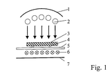
- Fig. 1 The arrangement shown in Fig. 1 consists of an aluminum mirror 1, which the light Xenon flash lamps 2 focused on the coated substrate 3 over the entire surface.
- the substrate 3 is supported on thin quartz rods 4 and by a quartz plate 5 from a preheating device, which consists of halogen lamps 6, separately.
- the performance of halogen lamps 6 is 2 kW.
- a further aluminum mirror 7 is attached below the halogen lamps 6.
- FIG. 2a there is a conventional one epitaxial deposition of an approximately 20-100 nm thick 3C-SiC epitaxial layer 9 a Si substrate 8.
- the layer system has the typical defects already described above 12, both in the 3C-SiC epitaxial layer 9, and in the silicon substrate 8, but in particular at the interface.
- the pane is first preheated to 600 - 800 ° C by the preheating device described in Fig. 1 and then exposed to a light pulse of 20 ms duration and an energy density of 100-150 Jcm -2 in a flash lamp system (sketched in Fig. 2 B).
- the coated substrate is under an argon atmosphere throughout the process.
- the light of the xenon flash lamps with an intensity maximum of the wavelength at about 500 nm is mainly absorbed in the layer system described in the region of the strongly disturbed SiC / Si interface and there causes the layer 10 to melt from the Si surface down to one Depth of a few 100 nanometers and the healing of defects 12 in Si and SiC depending on the radiated energy density.
- the end of the pulse begins due to the cooling of the Si substrate by thermal radiation the crystallization of the liquid Si film 10 epitaxially from the interface to solid silicon. Thereby heat is constantly released as latent heat, so that the solidification process thereby being delayed.
- the 3C-SiC epitaxial layer 9 Due to the thin layer and the high thermal conductivity of the materials, the 3C-SiC epitaxial layer 9 is present during the entire phase of melting and re-solidification of the silicon always at the melting temperature of the Silicon and only begins to cool when the entire Si layer as an intermediate form 11 is frozen again. Depending on how much silicon was melted, extended the annealing time of the 3C-SiC epitaxial layer 9 is proportional.
Landscapes
- Chemical & Material Sciences (AREA)
- Engineering & Computer Science (AREA)
- Crystallography & Structural Chemistry (AREA)
- Materials Engineering (AREA)
- Metallurgy (AREA)
- Organic Chemistry (AREA)
- Inorganic Chemistry (AREA)
- Chemical Kinetics & Catalysis (AREA)
- General Chemical & Material Sciences (AREA)
- Crystals, And After-Treatments Of Crystals (AREA)
Abstract
Description
Claims (7)
- Verfahren zur Behandlung heteroepitaktischer Halbleiterschichten auf Siliziumsubstraten, wobei Licht zur Behandlung eingesetzt wird, dadurch gekennzeichnet, dass die Oberfläche der Epitaxieschicht ganzflächig mit einem Lichtimpuls zwischen 2 und 500 ms der Energiedichte von 100 bis 200 Joule/cm2 und einem Intensitätsmaximum der Wellenlänge zwischen 400 und 600 nm bestrahlt wird.
- Verfahren nach Anspruch 1, dadurch gekennzeichnet, dass als heteroepitaktische Halbleiterschicht 3C-SiC eingesetzt wird.
- Verfahren nach Anspruch 1, dadurch gekennzeichnet, dass das beschichtete Siliziumsubstrat mit Hilfe einer Vorheizung, beispielsweise Halogenlampen, auf eine Temperatur, kleiner als die Schmelztemperatur des Siliziumsubstrates, also unter 1412 °C, vorgeheizt wird.
- Verfahren nach Anspruch 1, dadurch gekennzeichnet, dass anstelle eines Lichtimpulses mehrere zeitlich aufeinanderfolgende Lichtimpulse verwendet werden, wobei die Wartezeit zwischen den Impulsen zur Abkühlung des beschichteten Siliziumsubstrates genutzt wird.
- Verfahren nach Anspruch 4, dadurch gekennzeichnet, dass die Wartezeit zwischen den Lichtimpulsen zwischen 1 Sekunde und 10 Minuten beträgt.
- Verfahren nach Anspruch 4 , dadurch gekennzeichnet, dass der nachfolgende Lichtblitz gezündet wird, wenn die Temperatur des beschichteten Siliziumsubstrates 200 bis 1300 °C unter der maximalen Aufheiztemperatur liegt.
- Verfahren nach Anspruch 1 bis 6, dadurch gekennzeichnet, dass die Behandlung nach einer weiteren epitaktischen Abscheidung erneut vorgenommen wird.
Applications Claiming Priority (2)
| Application Number | Priority Date | Filing Date | Title |
|---|---|---|---|
| DE10127073A DE10127073A1 (de) | 2001-06-02 | 2001-06-02 | Verfahren zur Behandlung heteroepitaktischer Halbleiterschichten auf Siliziumsubstraten |
| DE10127073 | 2001-06-02 |
Publications (2)
| Publication Number | Publication Date |
|---|---|
| EP1263030A2 true EP1263030A2 (de) | 2002-12-04 |
| EP1263030A3 EP1263030A3 (de) | 2004-07-07 |
Family
ID=7687128
Family Applications (1)
| Application Number | Title | Priority Date | Filing Date |
|---|---|---|---|
| EP02012019A Withdrawn EP1263030A3 (de) | 2001-06-02 | 2002-05-31 | Verfahren zur Behandlung heteroepitaktischer Halbleiterschichten auf Siliziumsubstraten |
Country Status (2)
| Country | Link |
|---|---|
| EP (1) | EP1263030A3 (de) |
| DE (1) | DE10127073A1 (de) |
Cited By (2)
| Publication number | Priority date | Publication date | Assignee | Title |
|---|---|---|---|---|
| WO2006034672A3 (de) * | 2004-09-30 | 2006-09-21 | Forschungszentrun Rossendorf E | Verfahren zur behandlung von halbleitersubstraten, die mittels intensiven lichtimpulsen ausgeheilt werden |
| CN107924815A (zh) * | 2015-07-30 | 2018-04-17 | 威科仪器有限公司 | 在化学气相沉积系统中用于受控制掺杂物掺入和活化的方法和设备 |
Families Citing this family (2)
| Publication number | Priority date | Publication date | Assignee | Title |
|---|---|---|---|---|
| DE10344986B4 (de) * | 2003-09-27 | 2008-10-23 | Forschungszentrum Dresden - Rossendorf E.V. | Verfahren zur Erzeugung verbesserter heteroepitaktischer gewachsener Siliziumkarbidschichten auf Siliziumsubstraten |
| DE102005036669A1 (de) * | 2005-08-04 | 2007-02-08 | Forschungszentrum Rossendorf E.V. | Verfahren zur Behandlung von Halbleitersubstratoberflächen, die mittels intensiven Lichtimpulsen kurzzeitig aufgeschmolzen werden |
Family Cites Families (3)
| Publication number | Priority date | Publication date | Assignee | Title |
|---|---|---|---|---|
| DE19808246B4 (de) * | 1998-02-27 | 2004-05-13 | Daimlerchrysler Ag | Verfahren zur Herstellung eines mikroelektronischen Halbleiterbauelements mittels Ionenimplatation |
| DE19808245C1 (de) * | 1998-02-27 | 1999-06-24 | Daimler Chrysler Ag | Verfahren zur Herstellung eines mikroelektronischen Halbleiterbauelements |
| DE60045126D1 (de) * | 1999-06-25 | 2010-12-02 | Massachusetts Inst Technology | Oxidation einer auf einer germaniumschicht aufgebrachten siliziumschicht |
-
2001
- 2001-06-02 DE DE10127073A patent/DE10127073A1/de not_active Withdrawn
-
2002
- 2002-05-31 EP EP02012019A patent/EP1263030A3/de not_active Withdrawn
Cited By (3)
| Publication number | Priority date | Publication date | Assignee | Title |
|---|---|---|---|---|
| WO2006034672A3 (de) * | 2004-09-30 | 2006-09-21 | Forschungszentrun Rossendorf E | Verfahren zur behandlung von halbleitersubstraten, die mittels intensiven lichtimpulsen ausgeheilt werden |
| CN107924815A (zh) * | 2015-07-30 | 2018-04-17 | 威科仪器有限公司 | 在化学气相沉积系统中用于受控制掺杂物掺入和活化的方法和设备 |
| CN107924815B (zh) * | 2015-07-30 | 2019-08-13 | 威科仪器有限公司 | 在化学气相沉积系统中用于受控制掺杂物掺入和活化的方法和设备 |
Also Published As
| Publication number | Publication date |
|---|---|
| EP1263030A3 (de) | 2004-07-07 |
| DE10127073A1 (de) | 2002-12-12 |
Similar Documents
| Publication | Publication Date | Title |
|---|---|---|
| DE1933690C3 (de) | Verfahren zum Herstellen eines mindestens bereichsweise einkristallinen Films auf einem Substrat | |
| EP0328048B1 (de) | Herstellung von Halbleiterscheiben mit verbesserter Kontrolle der Innenstörstellen | |
| DE19640594B4 (de) | Bauelement | |
| DE112013002107B4 (de) | SiC-Einkristall-Herstellungsverfahren | |
| DE112015004143B4 (de) | Verfahren zum Herstellen eines Einkristalls, Verfahren zum Herstellen eines Siliziumwafers und Verfahren zur Herstellung eines Siliziumepitaxialwafers | |
| DE112009005154B4 (de) | Verfahren zum Erzeugen eines SiC-Einkristalls | |
| DE112018002163B4 (de) | Verfahren zur Herstellung eines Silicium-Einkristalls, Verfahren zur Herstellung eines epitaktischen Silicium-Wafers, Silicium-Einkristall, und epitaktischer Silicium-Wafer | |
| DE1084381B (de) | Legierungsverfahren zur Herstellung von pn-UEbergaengen an der Oberflaeche eines Halbleiterkoerpers | |
| DE3422750A1 (de) | Verfahren zum herstellen einer schicht aus einem mehrbestandteilmaterial | |
| DE2648053A1 (de) | Verfahren zum gleichmaessigen beschichten von keramischem material mit silizium | |
| DE102019003331B4 (de) | Halbleitersubstrat-herstellungssysteme und verwandte verfahren | |
| DE2153862C3 (de) | ||
| DE102015004603A1 (de) | Kombiniertes Waferherstellungsverfahren mit Laserbehandlung und temperaturinduzierten Spannungen | |
| DE3231671T1 (de) | Zuechtung von strukturen auf der basis von halbleitermaterialien der gruppe iv | |
| DE10127073A1 (de) | Verfahren zur Behandlung heteroepitaktischer Halbleiterschichten auf Siliziumsubstraten | |
| EP2859985A2 (de) | Waferherstellungsverfahren | |
| DE10127074A1 (de) | Verfahren zur Behandlung heteroepitaktischer Halbleiterschichten auf Silicon-on-insulator (SOI)-Substraten | |
| DE3002671C2 (de) | Verfahren zur Herstellung eines Siliciumcarbidsubstrats | |
| WO2023046427A1 (de) | Verfahren zur herstellung eines wachstumssubstrats, wachstumssubstrat, und verfahren zur herstellung einer vielzahl optoelektronischer halbleiterchips | |
| DE2301148A1 (de) | Verfahren zur herstellung einkristalliner halbleiterkoerper und halbleiteranordnungen, insbesondere strahlungsdetektoren, die derartige einkristalline halbleiterkoerper enthalten | |
| DE60036761T2 (de) | Einkristalliner SiC-Verbundwerkstoff für Halbleitereinrichtungen und Verfahren zu seiner Herstellung | |
| DE2547692C3 (de) | Verfahren zum Herstellen einer Halbleiteranordnung | |
| EP0843748B1 (de) | Verfahren zur herstellung von kristallinen schichten | |
| DE102020132900B4 (de) | Silizium-basierte Wafer und Verfahren zur Herstellung von Silizium-basierten Wafern | |
| DE10344986B4 (de) | Verfahren zur Erzeugung verbesserter heteroepitaktischer gewachsener Siliziumkarbidschichten auf Siliziumsubstraten |
Legal Events
| Date | Code | Title | Description |
|---|---|---|---|
| PUAI | Public reference made under article 153(3) epc to a published international application that has entered the european phase |
Free format text: ORIGINAL CODE: 0009012 |
|
| AK | Designated contracting states |
Kind code of ref document: A2 Designated state(s): AT BE CH CY DE DK ES FI FR GB GR IE IT LI LU MC NL PT SE TR |
|
| AX | Request for extension of the european patent |
Free format text: AL;LT;LV;MK;RO;SI |
|
| RAP1 | Party data changed (applicant data changed or rights of an application transferred) |
Owner name: FORSCHUNGSZENTRUM ROSSENDORF E.V. |
|
| PUAL | Search report despatched |
Free format text: ORIGINAL CODE: 0009013 |
|
| AK | Designated contracting states |
Kind code of ref document: A3 Designated state(s): AT BE CH CY DE DK ES FI FR GB GR IE IT LI LU MC NL PT SE TR |
|
| AX | Request for extension of the european patent |
Extension state: AL LT LV MK RO SI |
|
| RIC1 | Information provided on ipc code assigned before grant |
Ipc: 7C 30B 33/00 B Ipc: 7H 01L 21/20 A |
|
| AKX | Designation fees paid | ||
| REG | Reference to a national code |
Ref country code: DE Ref legal event code: 8566 |
|
| STAA | Information on the status of an ep patent application or granted ep patent |
Free format text: STATUS: THE APPLICATION IS DEEMED TO BE WITHDRAWN |
|
| 18D | Application deemed to be withdrawn |
Effective date: 20050111 |