EP1262818A2 - Rein optischer Schalter - Google Patents
Rein optischer Schalter Download PDFInfo
- Publication number
- EP1262818A2 EP1262818A2 EP02020000A EP02020000A EP1262818A2 EP 1262818 A2 EP1262818 A2 EP 1262818A2 EP 02020000 A EP02020000 A EP 02020000A EP 02020000 A EP02020000 A EP 02020000A EP 1262818 A2 EP1262818 A2 EP 1262818A2
- Authority
- EP
- European Patent Office
- Prior art keywords
- signal light
- polarized components
- horizontally polarized
- time difference
- propagation time
- Prior art date
- Legal status (The legal status is an assumption and is not a legal conclusion. Google has not performed a legal analysis and makes no representation as to the accuracy of the status listed.)
- Withdrawn
Links
- 230000010287 polarization Effects 0.000 claims abstract description 18
- 230000001939 inductive effect Effects 0.000 claims abstract description 7
- 230000003287 optical effect Effects 0.000 claims description 45
- 239000004065 semiconductor Substances 0.000 claims description 26
- 238000000034 method Methods 0.000 claims description 13
- 239000000463 material Substances 0.000 claims description 8
- 229910000980 Aluminium gallium arsenide Inorganic materials 0.000 claims description 2
- 238000005253 cladding Methods 0.000 claims description 2
- 230000009021 linear effect Effects 0.000 abstract description 24
- 230000007774 longterm Effects 0.000 abstract description 4
- 230000009022 nonlinear effect Effects 0.000 abstract description 2
- 230000000694 effects Effects 0.000 description 14
- 230000001427 coherent effect Effects 0.000 description 6
- 230000001419 dependent effect Effects 0.000 description 4
- 230000006798 recombination Effects 0.000 description 4
- 238000005215 recombination Methods 0.000 description 4
- 229910001218 Gallium arsenide Inorganic materials 0.000 description 3
- 238000010521 absorption reaction Methods 0.000 description 2
- 238000004891 communication Methods 0.000 description 2
- 238000005530 etching Methods 0.000 description 2
- 239000013307 optical fiber Substances 0.000 description 2
- 238000012545 processing Methods 0.000 description 2
- 238000009825 accumulation Methods 0.000 description 1
- BJQHLKABXJIVAM-UHFFFAOYSA-N bis(2-ethylhexyl) phthalate Chemical compound CCCCC(CC)COC(=O)C1=CC=CC=C1C(=O)OCC(CC)CCCC BJQHLKABXJIVAM-UHFFFAOYSA-N 0.000 description 1
- 239000000969 carrier Substances 0.000 description 1
- 238000007796 conventional method Methods 0.000 description 1
- 239000012792 core layer Substances 0.000 description 1
- 230000006866 deterioration Effects 0.000 description 1
- 238000005516 engineering process Methods 0.000 description 1
- 238000011835 investigation Methods 0.000 description 1
- 238000004519 manufacturing process Methods 0.000 description 1
- 238000012986 modification Methods 0.000 description 1
- 230000004048 modification Effects 0.000 description 1
- 230000010363 phase shift Effects 0.000 description 1
- 230000000087 stabilizing effect Effects 0.000 description 1
- 238000002834 transmittance Methods 0.000 description 1
- 230000005428 wave function Effects 0.000 description 1
Images


Classifications
-
- G—PHYSICS
- G02—OPTICS
- G02F—OPTICAL DEVICES OR ARRANGEMENTS FOR THE CONTROL OF LIGHT BY MODIFICATION OF THE OPTICAL PROPERTIES OF THE MEDIA OF THE ELEMENTS INVOLVED THEREIN; NON-LINEAR OPTICS; FREQUENCY-CHANGING OF LIGHT; OPTICAL LOGIC ELEMENTS; OPTICAL ANALOGUE/DIGITAL CONVERTERS
- G02F1/00—Devices or arrangements for the control of the intensity, colour, phase, polarisation or direction of light arriving from an independent light source, e.g. switching, gating or modulating; Non-linear optics
- G02F1/01—Devices or arrangements for the control of the intensity, colour, phase, polarisation or direction of light arriving from an independent light source, e.g. switching, gating or modulating; Non-linear optics for the control of the intensity, phase, polarisation or colour
- G02F1/21—Devices or arrangements for the control of the intensity, colour, phase, polarisation or direction of light arriving from an independent light source, e.g. switching, gating or modulating; Non-linear optics for the control of the intensity, phase, polarisation or colour by interference
-
- G—PHYSICS
- G02—OPTICS
- G02F—OPTICAL DEVICES OR ARRANGEMENTS FOR THE CONTROL OF LIGHT BY MODIFICATION OF THE OPTICAL PROPERTIES OF THE MEDIA OF THE ELEMENTS INVOLVED THEREIN; NON-LINEAR OPTICS; FREQUENCY-CHANGING OF LIGHT; OPTICAL LOGIC ELEMENTS; OPTICAL ANALOGUE/DIGITAL CONVERTERS
- G02F1/00—Devices or arrangements for the control of the intensity, colour, phase, polarisation or direction of light arriving from an independent light source, e.g. switching, gating or modulating; Non-linear optics
- G02F1/35—Non-linear optics
- G02F1/3515—All-optical modulation, gating, switching, e.g. control of a light beam by another light beam
- G02F1/3517—All-optical modulation, gating, switching, e.g. control of a light beam by another light beam using an interferometer
-
- G—PHYSICS
- G02—OPTICS
- G02F—OPTICAL DEVICES OR ARRANGEMENTS FOR THE CONTROL OF LIGHT BY MODIFICATION OF THE OPTICAL PROPERTIES OF THE MEDIA OF THE ELEMENTS INVOLVED THEREIN; NON-LINEAR OPTICS; FREQUENCY-CHANGING OF LIGHT; OPTICAL LOGIC ELEMENTS; OPTICAL ANALOGUE/DIGITAL CONVERTERS
- G02F1/00—Devices or arrangements for the control of the intensity, colour, phase, polarisation or direction of light arriving from an independent light source, e.g. switching, gating or modulating; Non-linear optics
- G02F1/01—Devices or arrangements for the control of the intensity, colour, phase, polarisation or direction of light arriving from an independent light source, e.g. switching, gating or modulating; Non-linear optics for the control of the intensity, phase, polarisation or colour
- G02F1/21—Devices or arrangements for the control of the intensity, colour, phase, polarisation or direction of light arriving from an independent light source, e.g. switching, gating or modulating; Non-linear optics for the control of the intensity, phase, polarisation or colour by interference
- G02F1/225—Devices or arrangements for the control of the intensity, colour, phase, polarisation or direction of light arriving from an independent light source, e.g. switching, gating or modulating; Non-linear optics for the control of the intensity, phase, polarisation or colour by interference in an optical waveguide structure
- G02F1/2257—Devices or arrangements for the control of the intensity, colour, phase, polarisation or direction of light arriving from an independent light source, e.g. switching, gating or modulating; Non-linear optics for the control of the intensity, phase, polarisation or colour by interference in an optical waveguide structure the optical waveguides being made of semiconducting material
-
- G—PHYSICS
- G02—OPTICS
- G02F—OPTICAL DEVICES OR ARRANGEMENTS FOR THE CONTROL OF LIGHT BY MODIFICATION OF THE OPTICAL PROPERTIES OF THE MEDIA OF THE ELEMENTS INVOLVED THEREIN; NON-LINEAR OPTICS; FREQUENCY-CHANGING OF LIGHT; OPTICAL LOGIC ELEMENTS; OPTICAL ANALOGUE/DIGITAL CONVERTERS
- G02F1/00—Devices or arrangements for the control of the intensity, colour, phase, polarisation or direction of light arriving from an independent light source, e.g. switching, gating or modulating; Non-linear optics
- G02F1/29—Devices or arrangements for the control of the intensity, colour, phase, polarisation or direction of light arriving from an independent light source, e.g. switching, gating or modulating; Non-linear optics for the control of the position or the direction of light beams, i.e. deflection
- G02F1/31—Digital deflection, i.e. optical switching
- G02F1/313—Digital deflection, i.e. optical switching in an optical waveguide structure
- G02F1/3136—Digital deflection, i.e. optical switching in an optical waveguide structure of interferometric switch type
Definitions
- the invention relates to an all-optical switch for directly controlling light with light, and more particularly to a ultra-fast all-optical switch to be used as an optical control element in the field of optical-fiber communication and optical data processing.
- a conventional optical control element has used the electro-optic control method in which optical control is carried out by electrical signals.
- the all-optical system in which optical control is carried out by a light has attracted attention as a method which enables higher speed operation of optical elements.
- the all-optical control system has many advantages such as that the operation speed thereof is not dependent on CR time constant of a circuit, and that it is possible to directly utilize optical pulses which enables to generate ultra-shorter pulses than electrical pulses.
- an all-optical device is based on non-linear refractive index changes regardless of configuration of the all-optical device.
- the rate and/or efficiency of the non-linear refractive index changes determines operation speed and energy of an all-optical device.
- Non-linear optical phenomena accompanying non-linear refractive index changes can be grouped into several groups; first of all, they are grouped as to whether they are resonantly enhanced phenomena or not. It is considered that the present technology could provide an all-optical device which is able to work at ultra-high repetition rate on the order of THz, if the purely nonresonant effects are utilized. However, the bar in such an all-optical device is that it needs significantly high optical power.
- the resonantly enhanced effects can be grouped as to whether they are coherent effects or not.
- the coherent effects mean the effects in which the correlation between a phase of a wave function of electronic system and a phase of a light is strictly maintained while a light interacts with a matter.
- the coherent effects occur on the condition that a pulse width of a light is shorter than the phase relaxation time of a matter which is, for instance, in the range of 0.1 to 0.2 picoseconds in bulk GaAs at room temperature.
- a pulse width of a light is longer than the phase relaxation time, real carrier generation occurs.
- the occurrence of real carrier generation requires excited electrons to longitudinally relax and, while reduces the operation speed of an all-optical device, and prevents occurrence of the coherent effects. If a pulse width of a light is shorter than the phase relaxation time, it is considered that the real carrier generation occurs due to two photon absorption and so on.
- a higher pulse repetition rate induces more remarkable accumulation of the real carrier generation.
- a ultra-fast phenomenon which can be observed with ultra-short pulses at a repetition rate of about 100 MHz generated by a mode-locked laser, will be unable to be observed due to the influence of the real carrier generation, if the repetition rate becomes much higher to exceed the carrier life time.
- the resonant incoherent effects caused by real carrier generation are quite practical, since it is considered that an all-optical device can be operated with low power below 1 Watt.
- the switch-off time or relaxation time of optical non-linear refractive index is dependent on the longitudinal relaxation time or interband recombination time of carrier. Since the interband recombination time is on the order of nanoseconds in GaAs, it is impossible to utilize the high-speed characteristic of a light.
- the invention provides an all-optical switch including (a) a device for introducing propagation time difference A to vertically and horizontally polarized components of a signal light, (b) a device for impressing phase modulation to the signal light, the device inducing refractive index changes when a control light is applied thereto, (c) a device for introducing propagation time difference B, which is opposite to the propagation time difference A, to the vertically and horizontally polarized components of the signal light, (d) a device for making polarization of the vertically and horizontally polarized components of the signal light to coincide with each other, and (e) a device for making the vertically and horizontally polarized components of the signal light to interfere with each other.
- the invention further provides an all-optical switch including (a) a device for splitting a signal light into vertically and horizontally polarized components, (b) a device for introducing propagation time difference A to the vertically and horizontally polarized components, (c) a device for combining the vertically and horizontally polarized components into a single signal light, (d) a device for impressing phase modulation to the signal light, the device inducing refractive index changes when a control light is applied thereto, (e) a device for splitting the signal light into vertically and horizontally polarized components, (f) a device for introducing propagation time difference B, which is opposite to the propagation time difference A, to the vertically and horizontally polarized components of the signal light, (g) a device for making polarization of the vertically and horizontally polarized components of the signal light to coincide with each other, and (h) a device for making the vertically and horizontally polarized components of the signal light to interfere with each other.
- the invention still further provides an all-optical switch including (a) a first polarizing beam splitter for splitting a signal light into vertically and horizontally polarized components, (b) a plurality of total reflection mirrors defining an optical path starting from the first polarizing beam splitter for introducing propagation time difference A to the vertically and horizontally polarized components, (c) a second polarizing beam splitter for combining the vertically and horizontally polarized components into a single signal light, (d) a semiconductor waveguide for impressing phase modulation to the signal light, the semiconductor waveguide inducing refractive index changes when a control light is applied thereto, (e) a third polarizing beam splitter for splitting the signal light into vertically and horizontally polarized components, (f) combination of a right-angled mirror and a corner cube, the right-angled mirror placed in an optical path of one of the vertically and horizontally polarized component of the signal light, the corner cube disposed so that it receives the one of the component reflected by
- the invention yet further provides an all-optical switch made up of a semiconductor chip, the semiconductor chip including (a) a first TE-TM splitter for splitting a signal light into vertically and horizontally polarized components, (b) a second TE-TM splitter for receiving the split components to combine them into a single beam, (c) a first optical path connecting the first TE-TM splitter to the second TE-TM splitter, (d) a second optical path connecting the first TE-TM splitter to the second TE-TM splitter, the second optical path being longer than the first optical path, the split components transmitting through the first and second optical paths to produce propagation time difference A therebetween, (e) a non-linear waveguide for impressing phase modulation to the signal light, the non-linear waveguide inducing refractive index changes when a control light is applied thereto, (f) a third TE-TM splitter for splitting the signal light into vertically and horizontally polarized components, (g) a third optical path for introducing propagation
- the invention provides a method of optical control including the steps of (a) introducing propagation time difference A to vertically and horizontally polarized components of a signal light, (b) impressing phase modulation to the signal light by introducing the signal light to material in which refractive index changes are induced when a control light is applied thereto, (c) introducing propagation time difference B, which is opposite to the propagation time difference A, to the vertically and horizontally polarized components of the signal light, (d) making polarization of the vertically and horizontally polarized components of the signal light to coincide with each other, and (e) making the vertically and horizontally polarized components of the signal light to interfere with each other.
- the invention further provides a method of optical control including the steps of (a) splitting a signal light into vertically and horizontally polarized components, (b) introducing propagation time difference A to the vertically and horizontally polarized components, (c) combining the vertically and horizontally polarized components into a single beam, (d) introducing the signal light to material in which refractive index changes are induced when a control light is applied thereto, to impress phase modulation to the signal light, (e) splitting the signal light into vertically and horizontally polarized components, (f) introducing propagation time difference B, which is opposite to the propagation time difference A, to the vertically and horizontally polarized components of the signal light, (g) making polarization of the vertically and horizontally polarized components of the signal light to coincide with each other, and (h) making the vertically and horizontally polarized components of the signal light to interfere with each other.
- the switching speed thereof is not restricted by slow relaxation time by which highly efficient non-linear optical effect is characterized, even if highly efficient band-filling effect is utilized.
- the all-optical switch in accordance with the invention requires only one non-linear waveguide unlike the conventional symmetric Mach-Zehnder type all-optical switch, resulting in better, long-term stability.
- highly sensitive non-linear refractive index effect to be utilized in the all-optical switch in accordance with the invention enables the all-optical switch to operate with low power.
- Fig. 1 illustrates the all-optical switch in accordance with the first embodiment of the present invention.
- first and second polarizing beam splitters (PBS) 1 and 2 are juxtaposed with each other. Since the signal light SL is polarized at an angle of 45 degrees relative to a plane of Fig. 1, the signal light SL is divided by the first polarizing beam splitter 1 into two components, that is, p-polarized component and s-polarized component.
- the horizontally polarized light is corresponding to the p-polarized light in the terminology used with the polarizing beam splitter.
- the p-polarized component is polarized horizontally, namely, in a plane of Fig.
- the s-polarized component is vertically polarized, and reflected by the first polarizing beam splitter 1.
- the reflected s-polarized component is twice reflected by total reflection mirrors 3 and 4, and thus enters the second polarizing beam splitter 4.
- the p- and s-polarized components are combined in the second polarizing beam splitter 2.
- the s-polarized component ran by different optical length from that of the p-polarized component. Accordingly, the difference in optical length between the p- and s-polarized components induces a propagation time difference between the p- and s-polarized components. This state is shown in Fig. 2-B, in which the p- and s-polarized components are separately illustrated for clarity, though they are combined with each other in fact.
- the combined p- and s-polarized components namely the signal light SL passes through a wavelength selection mirror 5, and then enters a single-mode semiconductor waveguide 6.
- the semiconductor waveguide 6 consists of GaAs core and AlGaAs claddings.
- a control light CL is reflected by the wavelength selection mirror 5, and then enters the semiconductor waveguide 6 together with the signal light SL.
- the signal light SL is selected to have a wavelength of 900 nanometers which is within the transparent wavelength band of the semiconductor waveguide 6, and the control light CL is selected to have a wavelength of 870 nanometers which is within the absorption wavelength band of the semiconductor waveguide 6.
- the control light CL is made up of ultra-short pulses having a full-width at half-maximum of 1 picosecond.
- the semiconductor waveguide 6 is excited by the control light CL, and thereby imparts the phase modulation as shown in Fig. 2-C to the signal light SL.
- the phase of the signal light SL is changed as shown in Fig. 2-D.
- Fig. 2-D only black pulses are subject to phase shift by ⁇ radians shown in Fig. 2-C.
- the signal light SL having passed the semiconductor waveguide 6 is split again by a third polarizing beam splitter 7 into p- and s-polarized components.
- the p-polarized component passes through the third polarizing beam splitter 7, while the s-polarized component is reflected by the third polarizing beam splitter 7.
- On an optical path of the p-polarized component is disposed a triangle-shaped right-angled mirror 11.
- Above the right-angled mirror 11 is also disposed a corner cube 12 so that it receives the p-polarized component reflected by the right-angled mirror 11.
- the right-angled mirror 11 cooperates with the corner cube 12 to form a light delay circuit.
- the p-polarized component having passed through the third polarizing component 7 is reflected by the right-angled mirror 11 and the corner cube 12 by four times.
- the light delay circuit consisting of the right-angled mirror 11 and the corner cube 12 imparts a propagation time difference to the p- and s-polarized components.
- the propagation time difference imparted by the light delay circuit is just opposite to the propagation time difference imparted by the pair of the total reflection mirrors 3 and 4 to the signal light SL.
- the structure of the light delay circuit is not limited to the combination of the right-angled mirror 11 and the corner cube 12. For instance, in place of them, four total reflection mirrors may be used.
- the s-polarized component reflected by the third polarizing beam splitter 7 is further reflected by total reflection mirrors 8 and 10. While the s-polarized component forwards from the mirror 8 to the mirror 10, the s-polarized component passes through a half-wave plate 9, thereby the s-polarized component is rotated in polarization to a p-polarized component. This state is shown in Fig. 2-E.
- the state of interference is reversed, and thereby the second pulses leave the half mirror 13 through the exit B.
- Third pulses are both subject to phase modulation by ⁇ radians, and thus they have no difference in phase. Accordingly, the third pulses leave the half mirror 13 through the exit A similarly to the first pulses.
- the all-optical switch in accordance with the invention utilizes the non-linear refractive index changes as shown in Fig. 2-C, the all-optical switch makes it possible to accomplish ultra-fast switching.
- the all-optical switch since the all-optical switch requires only one non-linear portion, which corresponds to the semiconductor waveguide 6 in the above described embodiment, the all-optical switch has an advantage of long-term stability.
- the all-optical switch is constructed of various optical components.
- the all-optical switch in accordance with the invention can be constructed also of a semiconductor chip.
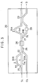
- Fig. 3 illustrates an all-optical switch 20 in accordance with the second embodiment of the present invention, which is made up of a semiconductor chip.
- the illustrated all-optical switch 20 includes a first TE-TM splitter 21 for splitting a received signal light SL into TE and TM polarized components, and a second TE-TM splitter 22 for receiving the TE and TM polarized components to combine them into a signal light SL again.
- the polarization states are designated as p- or s- polarization, but in waveguide they are referred to as TE or TM polarization.
- the first TE-TM splitter 21 is connected to the second TE-TM splitter 22 through first and second optical paths 30A and 30B through which the TE and TM polarized components are transmitted, respectively.
- the second optical path 30B is designed to be longer than the first optical path 30A.
- a control light CL is introduced into the all-optical switch through a wavelength selection coupler 25, and enters a non-linear waveguide 26 together with the signal light SL.
- the non-linear waveguide 26 induces refractive index changes by the control light CL applied thereto, and thus imparts phase modulation to the signal light SL.
- the signal light SL is split again into TE and TM polarized components by a third TE-TM splitter 27.
- the TM polarized component is transmitted through a third optical path 31A, while the TE polarized component is transmitted through a fourth optical path 31B.
- the TE polarized component is inverted in polarization to TM polarized component by a TE-TM converter 29 disposed on the fourth optical path.
- a difference in optical length between the third and fourth optical paths 31A and 31B imparts a propagation time difference to the TE and TM polarized components. This propagation time difference is just opposite to one imparted by the first and second optical paths 30A and 30B. Then, the TE and TM polarized components interfere with each other at a 3 dB coupler 23, and leaves the all-optical switch 20 through an exit A or B.
- the above mentioned elements are all formed on a wafer by etching.
- the etching is deeper than a core layer, and hence the all-optical switch 20 is designed to be of ridge type.
- the non-linear waveguide 26 may be of other types such as stripe-loaded type.
- the non-linear waveguide 26 includes a core having a narrower bandgap than the rest thereof by virtue of selective growth and regrowth.
- the non-linear waveguide 26 corresponds to the semiconductor waveguide 6 of the first embodiment illustrated in Fig. 1.
- the TE-TM splitters 21, 22 and 27 correspond to the polarizing beam splitters 1, 2 and 7 of the first embodiment, respectively.
- the wavelength selection coupler 25, the TE-TM converter 29 and the 3 dB coupler 23 correspond to and have the same function as the wavelength selection mirror 5, the half-wave plate 9 and the half mirror 13 of the first embodiment.
- the second embodiment illustrated in Fig. 3 has the same operation principle as that of the first embodiment illustrated in Fig. 1.
- the TE-TM splitters 21, 22 and 27 and the TE-TM converter 29 can be fabricated by arranging a difference in propagation constants of TE and TM modes of waveguides to be a certain value.
- GaAs family material is used in the above described embodiments, other materials such as InP, InGaAsP and GaAlAs may be used for each of wavelengths thereof.
- the embodiments utilize non-linear refractive index changes caused by band-filling effect of the semiconductor waveguide, the same effects can be obtained even by utilizing the non-linearity of a semiconductor into which carriers are introduced in the form of current, as suggested by R. J. Manning et al., Electronic Letters, Vol. 30, No. 10, pp 787-788, 1994.
- Other elements and components may be substituted for the optical elements and components used in the above described embodiments, if they provide the same function and effects as those of the optical elements and components of the embodiments.
Landscapes
- Physics & Mathematics (AREA)
- Nonlinear Science (AREA)
- General Physics & Mathematics (AREA)
- Optics & Photonics (AREA)
- Optical Modulation, Optical Deflection, Nonlinear Optics, Optical Demodulation, Optical Logic Elements (AREA)
- Optical Integrated Circuits (AREA)
Applications Claiming Priority (3)
| Application Number | Priority Date | Filing Date | Title |
|---|---|---|---|
| JP32080194 | 1994-12-22 | ||
| JP6320801A JP2629624B2 (ja) | 1994-12-22 | 1994-12-22 | 全光スイッチ |
| EP95119591A EP0718669B1 (de) | 1994-12-22 | 1995-12-12 | Rein optischer Schalter |
Related Parent Applications (1)
| Application Number | Title | Priority Date | Filing Date |
|---|---|---|---|
| EP95119591A Division EP0718669B1 (de) | 1994-12-22 | 1995-12-12 | Rein optischer Schalter |
Publications (2)
| Publication Number | Publication Date |
|---|---|
| EP1262818A2 true EP1262818A2 (de) | 2002-12-04 |
| EP1262818A3 EP1262818A3 (de) | 2003-04-23 |
Family
ID=18125397
Family Applications (2)
| Application Number | Title | Priority Date | Filing Date |
|---|---|---|---|
| EP95119591A Expired - Lifetime EP0718669B1 (de) | 1994-12-22 | 1995-12-12 | Rein optischer Schalter |
| EP02020000A Withdrawn EP1262818A3 (de) | 1994-12-22 | 1995-12-12 | Rein optische Schaltervorrichtung |
Family Applications Before (1)
| Application Number | Title | Priority Date | Filing Date |
|---|---|---|---|
| EP95119591A Expired - Lifetime EP0718669B1 (de) | 1994-12-22 | 1995-12-12 | Rein optischer Schalter |
Country Status (4)
| Country | Link |
|---|---|
| US (1) | US5710845A (de) |
| EP (2) | EP0718669B1 (de) |
| JP (1) | JP2629624B2 (de) |
| DE (1) | DE69531335T2 (de) |
Families Citing this family (26)
| Publication number | Priority date | Publication date | Assignee | Title |
|---|---|---|---|---|
| JP3751052B2 (ja) * | 1994-12-28 | 2006-03-01 | シャープ株式会社 | 集積型光制御素子およびその作製方法、並びにそれを備えた光集積回路素子および光集積回路装置 |
| KR100483981B1 (ko) | 1996-02-22 | 2005-11-11 | 가부시키가이샤 니콘 | 펄스폭신장광학계및이러한광학계를갖춘노광장치 |
| JPH10301151A (ja) * | 1997-04-28 | 1998-11-13 | Nec Corp | 波長変換器 |
| JP3439345B2 (ja) | 1998-06-29 | 2003-08-25 | 日本電気株式会社 | 波長変換器及び波長変換方法 |
| JP3391267B2 (ja) | 1998-07-14 | 2003-03-31 | 日本電気株式会社 | 全光スイッチ及び波長変換器 |
| JP3186704B2 (ja) | 1998-08-05 | 2001-07-11 | 日本電気株式会社 | 半導体非線形導波路及び光スイッチ |
| US6314215B1 (en) | 1998-09-17 | 2001-11-06 | New Mexico State University Technology Transfer Corporation | Fast all-optical switch |
| US6556742B2 (en) * | 1998-11-04 | 2003-04-29 | Fujitsu Limited | Optical wavelength division multiplexed system using wavelength splitters |
| US6721508B1 (en) * | 1998-12-14 | 2004-04-13 | Tellabs Operations Inc. | Optical line terminal arrangement, apparatus and methods |
| US6298180B1 (en) | 1999-09-15 | 2001-10-02 | Seng-Tiong Ho | Photon transistors |
| US6473541B1 (en) | 1999-09-15 | 2002-10-29 | Seng-Tiong Ho | Photon transistors |
| US6694066B2 (en) * | 2001-02-14 | 2004-02-17 | Finisar Corporation | Method and apparatus for an optical filter |
| US6603904B1 (en) | 2001-03-28 | 2003-08-05 | Jaffalight Holdings Llc | All optical narrow pulse generator and switch for dense time division multiplexing and code division multiplexing |
| US7106508B2 (en) * | 2001-06-11 | 2006-09-12 | Finisar Corporation | Hybrid cell |
| US7005669B1 (en) | 2001-08-02 | 2006-02-28 | Ultradots, Inc. | Quantum dots, nanocomposite materials with quantum dots, devices with quantum dots, and related fabrication methods |
| US6710366B1 (en) | 2001-08-02 | 2004-03-23 | Ultradots, Inc. | Nanocomposite materials with engineered properties |
| US6794265B2 (en) * | 2001-08-02 | 2004-09-21 | Ultradots, Inc. | Methods of forming quantum dots of Group IV semiconductor materials |
| US6819845B2 (en) | 2001-08-02 | 2004-11-16 | Ultradots, Inc. | Optical devices with engineered nonlinear nanocomposite materials |
| US20030066998A1 (en) * | 2001-08-02 | 2003-04-10 | Lee Howard Wing Hoon | Quantum dots of Group IV semiconductor materials |
| US20040062465A1 (en) * | 2002-10-01 | 2004-04-01 | Woodley Bruce Robert | Apparatus and method for measuring optical power as a function of wavelength |
| US7432517B2 (en) * | 2004-11-19 | 2008-10-07 | Asml Netherlands B.V. | Pulse modifier, lithographic apparatus, and device manufacturing method |
| JP4482603B2 (ja) * | 2005-11-01 | 2010-06-16 | ジ・アリゾナ・ボード・オブ・リージェンツ・オン・ビハーフ・オブ・ザ・ユニバーシティ・オブ・アリゾナ | 偏光カップリングキューブコーナー型再帰反射体 |
| JP4911404B2 (ja) | 2006-08-25 | 2012-04-04 | 独立行政法人産業技術総合研究所 | 光信号処理回路 |
| CN103837995B (zh) * | 2014-03-24 | 2015-12-30 | 电子科技大学 | 一种多路等差光延时系统 |
| CN109709685A (zh) * | 2019-03-14 | 2019-05-03 | 曲阜师范大学 | 一种非偏振激光转线偏振激光的装置 |
| CN112558334A (zh) * | 2020-12-01 | 2021-03-26 | 中国科学院上海光学精密机械研究所 | 一种超快光开关及光调制的结构 |
Family Cites Families (6)
| Publication number | Priority date | Publication date | Assignee | Title |
|---|---|---|---|---|
| GB9006675D0 (en) * | 1990-03-26 | 1990-05-23 | British Telecomm | Optical apparatus |
| DE4021293A1 (de) * | 1990-07-04 | 1992-01-16 | Deutsche Forsch Luft Raumfahrt | Bistabiler optischer schalter |
| US5305136A (en) * | 1992-03-31 | 1994-04-19 | Geo-Centers, Inc. | Optically bidirectional fast optical switch having reduced light loss |
| US5317658A (en) * | 1992-04-06 | 1994-05-31 | At&T Bell Laboratories | Apparatus and method for providing a polarization independent optical switch |
| JP2531443B2 (ja) * | 1993-07-02 | 1996-09-04 | 日本電気株式会社 | 全光素子 |
| US5455877A (en) * | 1994-10-27 | 1995-10-03 | Bell Communications Research, Inc. | Multi-channel wavelength-routing switch using acousto-optic polarization converters |
-
1994
- 1994-12-22 JP JP6320801A patent/JP2629624B2/ja not_active Expired - Fee Related
-
1995
- 1995-12-12 EP EP95119591A patent/EP0718669B1/de not_active Expired - Lifetime
- 1995-12-12 EP EP02020000A patent/EP1262818A3/de not_active Withdrawn
- 1995-12-12 DE DE69531335T patent/DE69531335T2/de not_active Expired - Lifetime
- 1995-12-20 US US08/580,061 patent/US5710845A/en not_active Expired - Fee Related
Non-Patent Citations (2)
| Title |
|---|
| LAGASSE M J ET AL: "Femtosecond all-optical switching in AlGaAs waveguides using a time division interferometer" APPLIED PHYSICS LETTERS, 22 MAY 1989, USA, vol. 54, no. 21, pages 2068-2070, XP000080568 ISSN 0003-6951 * |
| LAGASSE M J ET AL: "Ultrafast switching with a single-fiber interferometer" OPTICS LETTERS, 15 MARCH 1989, USA, vol. 14, no. 6, pages 311-313, XP000054172 ISSN 0146-9592 * |
Also Published As
| Publication number | Publication date |
|---|---|
| DE69531335T2 (de) | 2004-04-15 |
| EP0718669A3 (de) | 1996-12-04 |
| JP2629624B2 (ja) | 1997-07-09 |
| EP0718669B1 (de) | 2003-07-23 |
| JPH08179385A (ja) | 1996-07-12 |
| EP1262818A3 (de) | 2003-04-23 |
| US5710845A (en) | 1998-01-20 |
| EP0718669A2 (de) | 1996-06-26 |
| DE69531335D1 (de) | 2003-08-28 |
Similar Documents
| Publication | Publication Date | Title |
|---|---|---|
| US5710845A (en) | All-optical switch | |
| EP0632313B1 (de) | Rein optische Vorrichtung | |
| Jewell et al. | 3‐pJ, 82‐MHz optical logic gates in a room‐temperature GaAs‐AlGaAs multiple‐quantum‐well étalon | |
| Nakamura et al. | Ultrafast (200-fs switching, 1.5-Tb/s demultiplexing) and high-repetition (10 GHz) operations of a polarization-discriminating symmetric Mach-Zehnder all-optical switch | |
| Kotb et al. | 100 Gb/s all-optical multifunctional AND, NOR, XOR, OR, XNOR, and NAND logic gates in a single compact scheme based on semiconductor optical amplifiers | |
| Asobe et al. | Ultrafast all-optical switching using highly nonlinear chalcogenide glass fiber | |
| US5742415A (en) | Optical switching device | |
| Gayen et al. | Designing of optimized all-optical half adder circuit using single quantum-dot semiconductor optical amplifier assisted Mach-Zehnder interferometer | |
| HK1010064B (en) | Optical switching device | |
| Thomas et al. | Physics in the whirlwind of optical communications | |
| Liu et al. | A wavelength tunable optical buffer based on self-pulsation in an active microring resonator | |
| Soto et al. | All-optical NOR gates with two and three input logic signals based on cross-polarization modulation in a semiconductor optical amplifier | |
| Taranenko et al. | Spatial solitons in semiconductor microresonators | |
| Chen et al. | Single‐mode polymer waveguide modulator | |
| Smith et al. | Materials for all-optical devices | |
| US6498885B1 (en) | Semiconductor nonlinear waveguide and optical switch | |
| JP2705671B2 (ja) | 光スイッチの駆動方法および光スイッチ | |
| RU2153688C2 (ru) | Способ переключения, модуляции, усиления и управления и нелинейный оптический переключатель, модулятор, усилитель и управляющий элемент | |
| Tanabe et al. | Ultrahigh-Q photonic crystal nanocavities and their applications | |
| JP2978503B2 (ja) | 全光学型光制御素子 | |
| NAKATSUHARA et al. | GaInAsP/InP directional coupler loaded with grating for optically-controlled switching | |
| Cada et al. | Optical nonlinear devices | |
| Stegeman | All-optical switching | |
| Tajrma et al. | 24 ps switching with a Mach-Zehnder type all-optical switch based on the band filling nonlinearity of GaAs | |
| Takenouchi et al. | Differential processing using an arrayed-waveguide grating |
Legal Events
| Date | Code | Title | Description |
|---|---|---|---|
| PUAI | Public reference made under article 153(3) epc to a published international application that has entered the european phase |
Free format text: ORIGINAL CODE: 0009012 |
|
| AC | Divisional application: reference to earlier application |
Ref document number: 718669 Country of ref document: EP |
|
| AK | Designated contracting states |
Kind code of ref document: A2 Designated state(s): DE FR GB |
|
| PUAL | Search report despatched |
Free format text: ORIGINAL CODE: 0009013 |
|
| AK | Designated contracting states |
Designated state(s): DE FR GB |
|
| RIC1 | Information provided on ipc code assigned before grant |
Ipc: 7G 02F 1/313 B Ipc: 7G 02F 1/225 B Ipc: 7G 02F 1/21 B Ipc: 7G 02F 1/35 A |
|
| 17P | Request for examination filed |
Effective date: 20030311 |
|
| 17Q | First examination report despatched |
Effective date: 20030617 |
|
| AKX | Designation fees paid |
Designated state(s): DE FR GB |
|
| 17Q | First examination report despatched |
Effective date: 20030617 |
|
| STAA | Information on the status of an ep patent application or granted ep patent |
Free format text: STATUS: THE APPLICATION HAS BEEN WITHDRAWN |
|
| 18W | Application withdrawn |
Effective date: 20060724 |